Normal view

There are new articles available, click to refresh the page.
Before yesterdayKen+Shirriff's+blog

The adder at the heart of Intel's 8087 floating-point chip

13 June 2026 at 15:56

In 1980, Intel released the Intel 8087 floating-point coprocessor, a chip that could make math up to 100 times faster. As well as arithmetic and square roots, the 8087 computed transcendental functions including tangent, exponentiation, and logarithms. But it all depended on a 69-bit adder: "The arithmetic heart of the floating-point execution unit is centered about a nanomachine comprised of the adder and its related registers, shifters and control circuitry," as the patent describes it. In this article, I explain the circuitry of this adder.

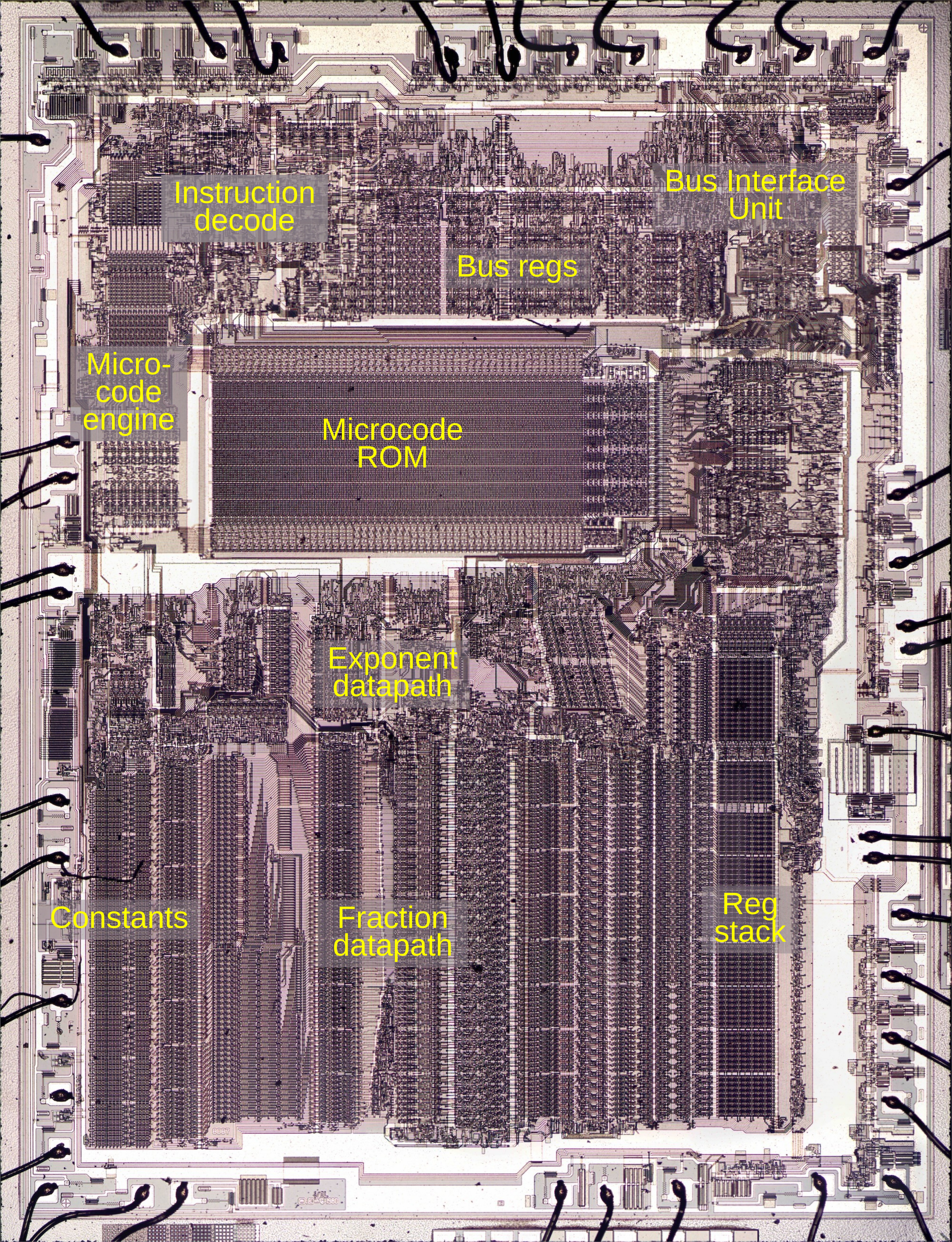
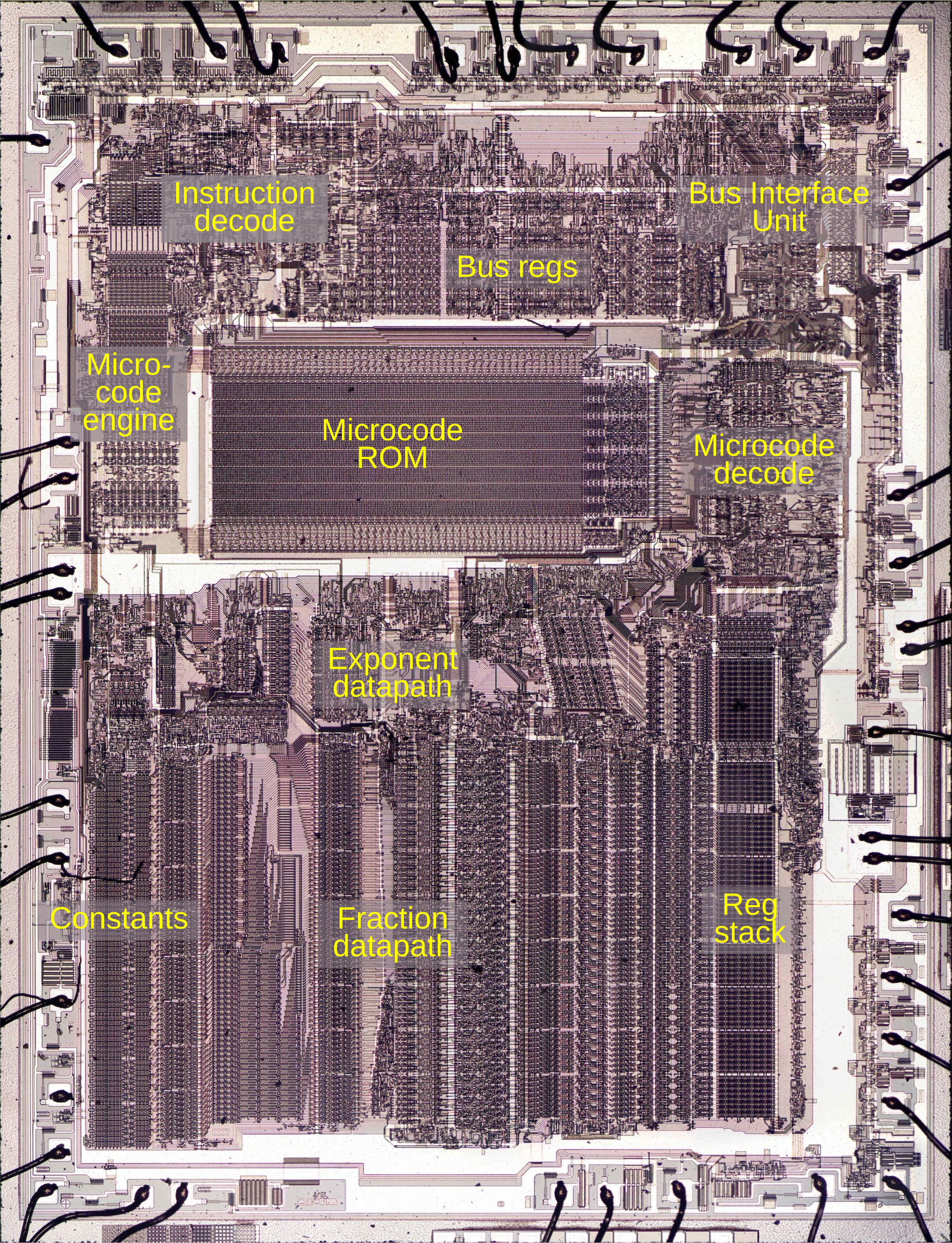
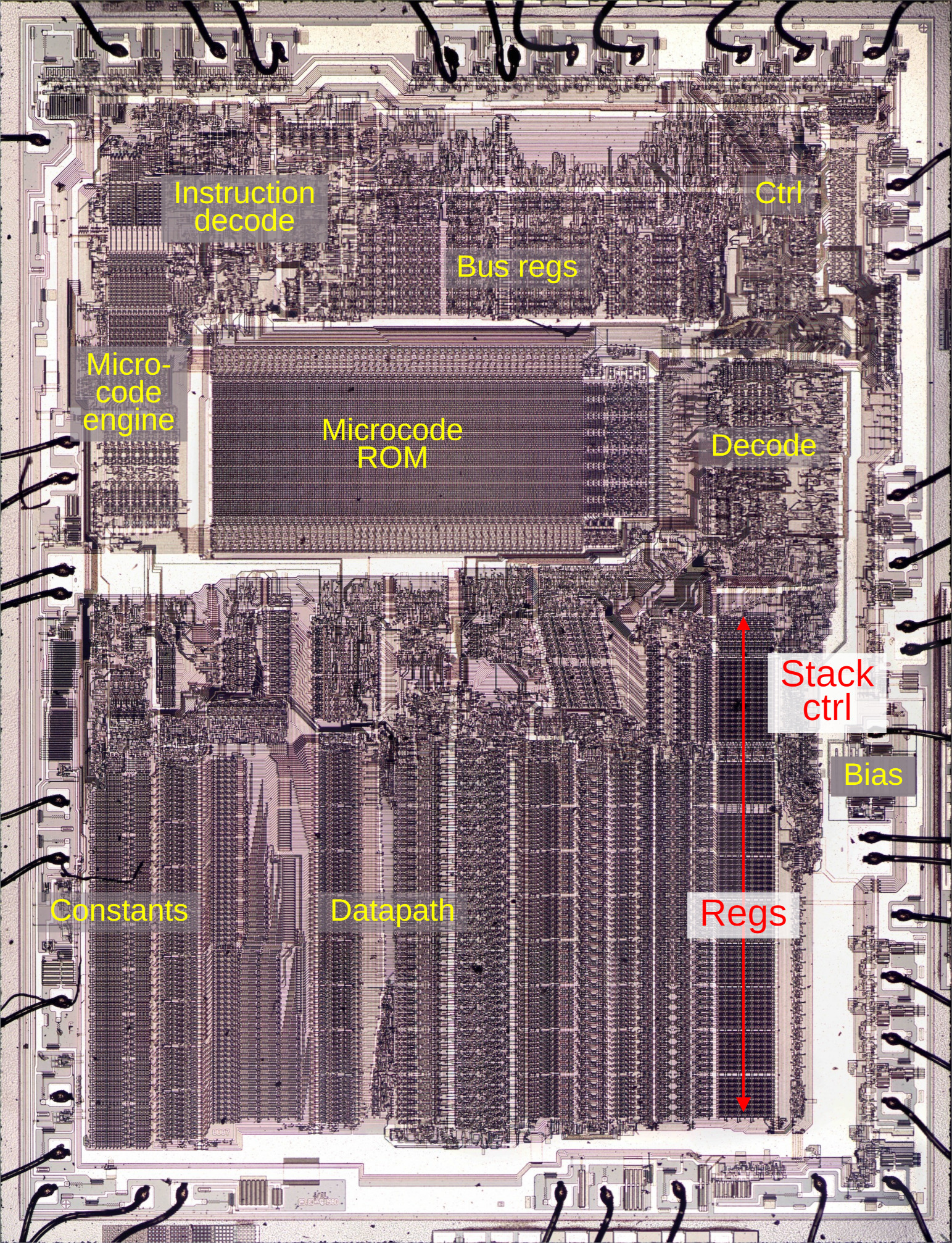
The photo below shows the 8087 die under a microscope. Around the edges of the die, hair-thin bond wires connect the chip to its 40 external pins. The complex patterns on the die are formed by its metal wiring, as well as the polysilicon and silicon underneath. At the top of the chip, the Bus Interface Unit connects to the rest of the system: coordinating with the main 8086 processor and memory. The chip's instructions are defined by the large microcode ROM in the middle.
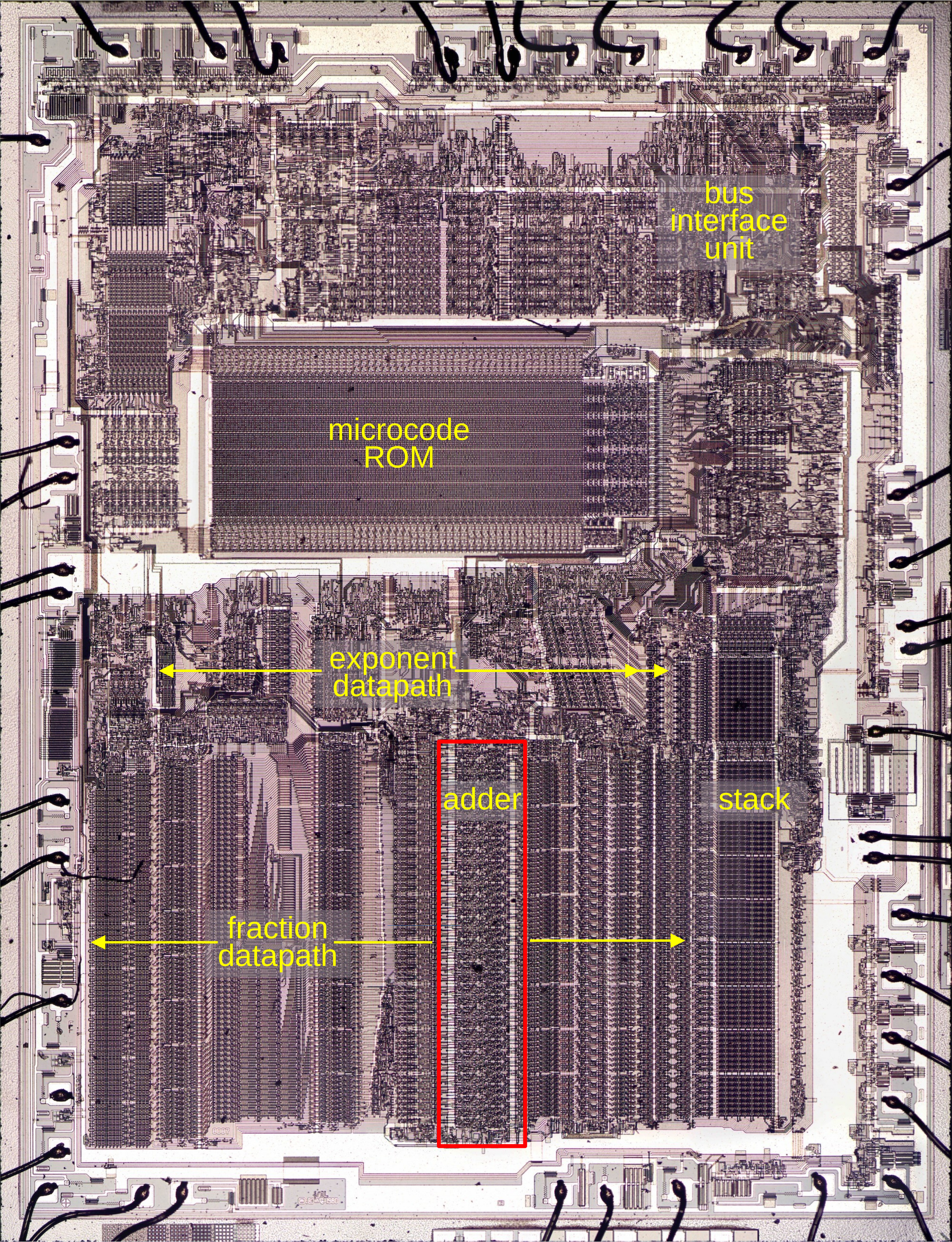
Die of the Intel 8087 floating-point unit chip, with relevant functional blocks labeled. The die is 5mm×6mm.  Click for a larger image.

Die of the Intel 8087 floating-point unit chip, with relevant functional blocks labeled. The die is 5mm×6mm. Click for a larger image.

The bottom half of the die is the "datapath", the circuitry that performs calculations; it is split into the exponent datapath, which handles the exponent of a floating-point number, and the fraction datapath, which handles the fractional part (or significand). The adder (red) sits in the middle of the fraction datapath; to perform addition on the exponent, the exponent must be copied over to the fraction datapath.

Structure of the adder

Building a binary adder is easy; the hard part is making it fast. The key problem is how to handle the carries from a bit position to the next. Each carry potentially depends on all the lower carries, but you don't want to wait as a carry ripples through the logic for all 69 bits. (It's similar to doing 999999+1 with long addition: you need to carry the one, carry the one, ...)

The 8087's adder speeds up performance by breaking addition into 4-bit blocks, using two techniques to make computation inside each block fast. The carry needs to ripple from block to block, but this reduces the number of carry steps by a factor of four.
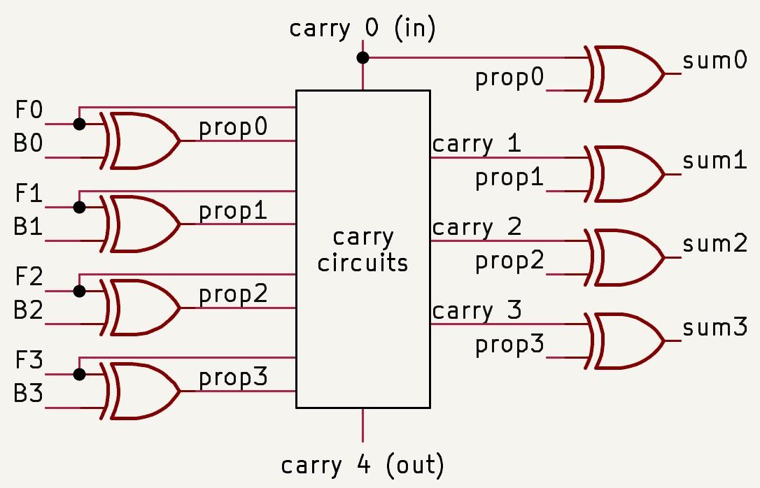
Simplified diagram of a four-bit block in the 8087's adder.

Simplified diagram of a four-bit block in the 8087's adder.

The diagram above shows the structure of one 4-bit block, with the carry generation circuits abstracted out for now. The adder takes two inputs: one (F) is from the chip's fraction bus, a bus that connects the components of the fraction datapath. The second input (B) comes from a register called the B register. Each bit of the sum is produced by XORing a F input, a B input, and the carry into that bit position.1 For reasons that will be explained below, the intermediate value (F XOR B) is called "propagate". The carry-out from each block is tied to the carry-in of the next block. But what happens inside the carry circuits?

In 1959, researchers at the University of Manchester developed a fast carry technique for a computer called Atlas. This technique, named the Manchester carry chain, computes the carry values by setting up switches in parallel and then letting the carry quickly propagate through the wires, controlled by the switches. Although the carry still needs to travel from bit to bit, it travels at the speed of a signal in a wire, not slowed by logic gates.2

The Manchester carry chain is built around the concepts of Generate, Propagate, and Delete (also known as Kill), which arise when adding two bits and a carry. If you add 1+1, a carry-out is generated, whether there is a carry-in or not. In contrast, if you add 0+0, there is no carry-out, regardless of the carry-in; any carry-in is deleted. The interesting case is if you add 0+1: a carry-out results only if there is a carry-in; that is, the carry-in is propagated to the carry-out. In logic terms, the generate signal is the AND of the two input bits, the delete signal is the NOR, and the propagate signal is the XOR. The important thing is that these signals can be computed for all bit positions in parallel, in constant time.
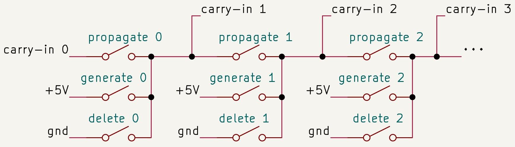
The idea behind the Manchester carry chain. Note that the low bit is on the left, so the carry flows left to right.

The idea behind the Manchester carry chain. Note that the low bit is on the left, so the carry flows left to right.

The Manchester carry chain is constructed as above, with the switches at each bit set according to the Generate/Propagate/Delete values. Once the switches are set, the carry status quickly flows through the circuit, producing the carry value at each position without any logic delays. If the propagate switch is closed, the previous carry passes through. But if the generate or delete switch is closed, the carry is set or cleared, respectively. Once the carry values are available, the final sum can be computed in parallel with XORs.

The 8087 uses an optimized circuit for the Manchester carry chain, combining the Generate and Delete cases. One stage of the adder's carry chain is shown below. For the propagate case, the carry-in Cin passes through the top switch, propagated to the carry out Cout. For the generate and delete cases, the bottom switch is closed, passing the input bit F. The trick is that the generate case corresponds to 1+1, so F is 1, resulting in Cout getting set. The delete case corresponds to 0+0, so F is 0, and Cout is cleared. (Note that both inputs, F and B, are the same in these cases, so using F instead of B is arbitrary.)
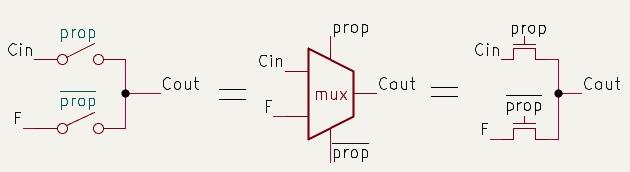
One stage of the Manchester carry chain.

One stage of the Manchester carry chain.

The middle of the diagram shows how the switches correspond to a multiplexer (mux) selecting the top signal Cin if prop is set, or the bottom signal F if prop is clear. The right side of the diagram shows the physical implementation with two NMOS transistors. These transistors function as switches (pass transistors), controlled by the prop signals on the gate.

The problem is that pass transistors aren't perfect switches, but lose a bit of voltage at each step. To fix this, the carry chain is broken into blocks of four bits (as shown earlier) and each block produces a "fresh" carry. This refresh is done by a "carry-skip" circuit, which can skip the carry processing inside the block. Specifically, the carry-skip mechanism checks if all positions inside the block are Propagate. In this case, the carry-out will have the same value as the carry-in (since the carry-in propagates through all the bit positions of the block). The carry-skip circuit detects this case and produces a carry-out signal matching the carry-in.

Putting this all together, the schematic below shows the adder circuitry for a typical block of four bits. The four multiplexers form the Manchester carry chain, while the NOR gate detects the carry-skip case.
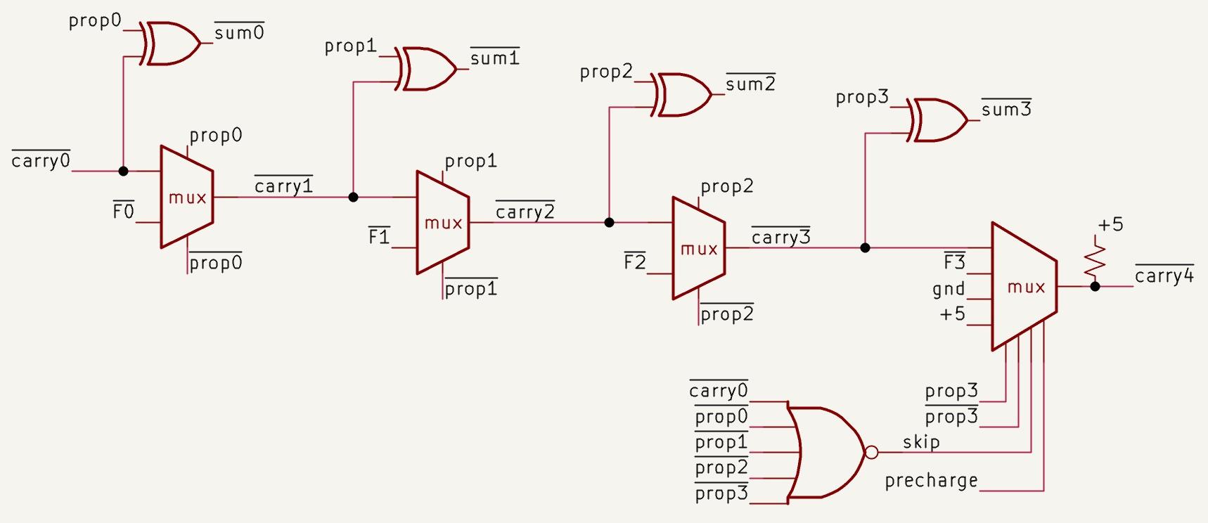
Reverse-engineered schematic for a 4-bit block of the adder.

Reverse-engineered schematic for a 4-bit block of the adder.

To optimize performance, there is a complication for electrical reasons.3 The 8087 uses NMOS transistors, which are much faster to pull a signal low than to pull a signal high. To improve performance, the carry lines are precharged to 5V at the start of an addition, and then the circuitry pulls the lines low if needed. In order to start in the no-carry state, the carry lines are all negated, so the initial 5V state corresponds to no carry, and the ground state corresponds to a carry.

The last multiplexer in the block has four inputs instead of two4. The third input pulls the (inverted) carry line low for the carry skip case.5 The fourth input is the precharge signal; it puts 5V on the carry line to precharge it. (A control circuit activates the precharge signal at the start of an addition cycle.) Note that this only precharges one of the carry lines; to precharge the rest, the propagate signal is forced high during precharge.
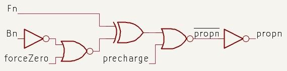
Reverse-engineered schematic for the propagate circuit. This shows an arbitrary bit n.

Reverse-engineered schematic for the propagate circuit. This shows an arbitrary bit n.

The circuit to generate the propagate signal (above) is conceptually the XOR of the two inputs, but there are (of course) complications. When the precharge signal is high, propagate is forced high, tying all the carry lines together so the precharge can propagate to all of them. The second feature is that the B inputs can be blocked by the forceZero signal, so the value 0 is added instead of the B value.

To summarize, the adder is divided into blocks of four bits. Each block uses a Manchester carry chain and a carry-skip circuit to optimize the performance. Even with these optimizations, though, the large number of blocks requires the 8087 to take two clock cycles to complete an addition.

The adder in silicon

The image below shows how the circuitry for a block of four bits appears on the die. These blocks are stacked vertically to create the complete adder as seen in the earlier die photo. In this image, the metal layer is visible as white lines, mostly obscuring the circuitry underneath. The 8087 has a single metal layer, which constrains the layout. Note that metal wiring is tightly packed, occupying almost the complete area. The thick vertical metal trace at the left is ground, while the thick metal trace at the right is power, supplying the adder circuitry. The horizontal traces provide wiring inside the adder block, as well as allowing the fraction bus to pass across the adder. The vertical lines on either side are control signals for the adder (precharge and forceZero) as well as connections to circuitry at the bottom of the chip.
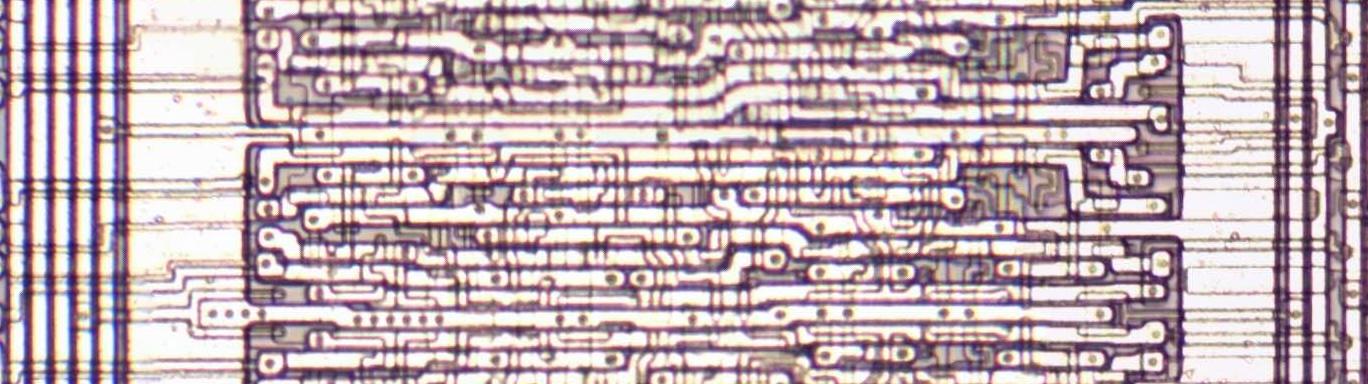
A block of four bits in the adder.

A block of four bits in the adder.

The photo below shows the silicon and polysilicon circuitry underneath the metal layer. (To take this photo, I dissolved the metal layer with acid.) The thin lines are polysilicon wiring, while the pinkish areas that appear raised are doped silicon. A transistor is formed when polysilicon crosses doped silicon. The circuitry is complex and irregular, connected by the horizontal metal wires above. The white circuits are contacts between the silicon and the metal wiring, while the white squares are contacts between the polysilicon and metal. Roughly speaking, if you divide the circuitry above into quarters, each quarter adds one bit. The carry-skip circuitry is in the middle.
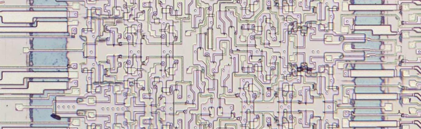
A block of four bits in the adder with the metal layer removed.

A block of four bits in the adder with the metal layer removed.

The left and the right sides of the image don't have any transistors, just polysilicon lines that pass under the vertical metal wiring. Many of these polysilicon lines are widened to reduce their resistance and thus tune performance. The silicon in these regions is "wasted", just providing a channel for the vertical wiring.

The size of the adder

Although the 8087 nominally has 64-bit values for the fraction (significand), the adder is slightly larger: it takes 69 bits as input and generates 70 output bits. One reason is that the 8087 uses three extra low-order bits for rounding, called Guard, Round, and Sticky. These bits ensure that a value is always rounded in the right direction. Handling of the rounding bits is fairly complicated, with multiple modes, but from the adder's perspective they are just three input bits.6

As will be explained below, the value from the B register can be doubled, requiring one more bit. Finally, the fraction bus and the B value can be negated. (This is used for subtraction, among other things.) A negative value is represented in two's complement, requiring one more bit. In total, the inputs to the adder are 69 bits wide.

When adding two large numbers, the result can require one additional bit. Thus, the output of the adder is 70 bits wide. The Sum Shifter (explained below) can shift the output two bits to the right, cutting the result down to 68 bits. This is still one bit larger than 64 bits with 3 rounding bits; the "extra" bit is supported by a few special-purpose registers, such as the tmpC register7 and the Skip Shifter.

The surrounding circuitry

The inputs and outputs of the adder are tied to some special registers and circuits. I'll leave a detailed explanation of this circuitry to another post, but I'll provide a brief description here.8 The adder has two inputs: one input is from the fraction bus and the other input is from the B register. The adder's output is stored in the Sum Register. To make multiplication faster, the 8087 uses radix-4 Booth multiplication, which multiplies by two bits at a time. The multiplier is stored in the Skip Shifter, a register that allows two bits to be shifted out at a time. Based on these bits, one of the values 2B, B, 0, or -B is added. (The -B path is also used for subtraction.) The adder's output is shifted right two bits by the Sum Shifter (not to be confused with the Skip Shifter) and stored in the Sum Register.
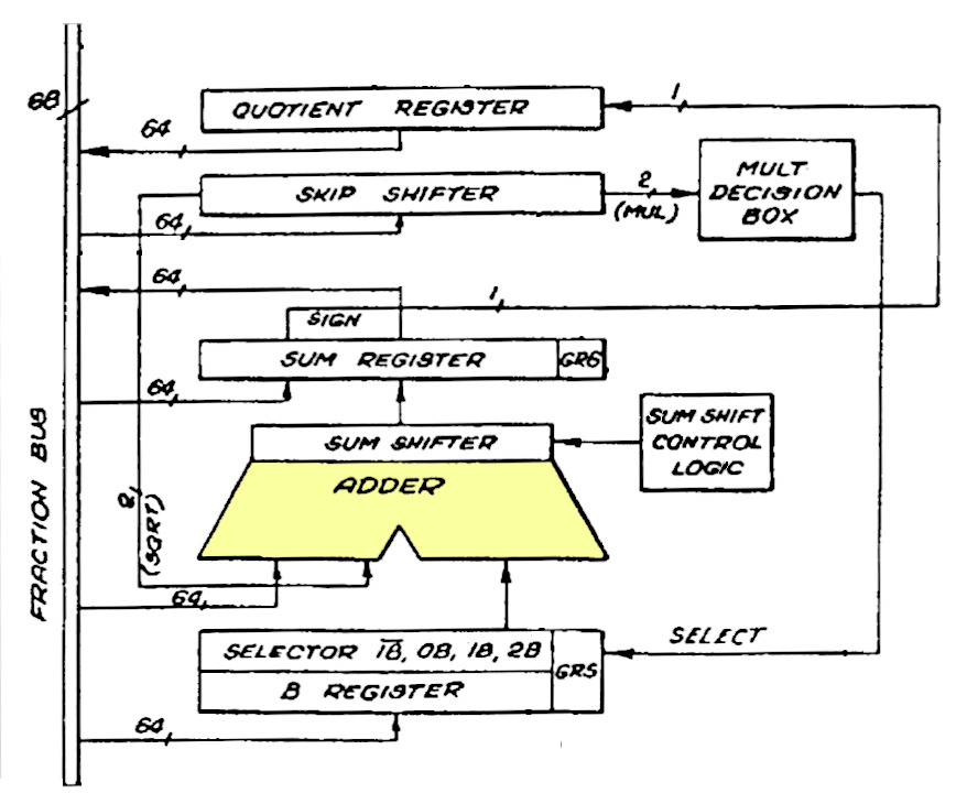
The adder and associated registers. Based on the patent.

The adder and associated registers. Based on the patent.

Division is implemented by repeated subtraction, addition, and shifting. The bits of the result are accumulated in the quotient register. The implementation of square root is similar to the pencil-and-paper long square root, except in binary. The skip shifter provides two bits from the left, which are appended to the right side of the adder input. A subtract or add takes place, similar to division, and the square root is formed in the B register.

Multiplication, division, and square root require multiple steps to process all the bits. For performance, this looping is implemented in hardware, not in microcode. These instructions require a lot of microcode to prepare the arguments, handle exponents, handle special cases, and store the results, but the inner loop is hardware.

Conclusions

The 8087 patent expresses the importance of the adder: "Ultimately, all arithmetical operations are reduced at one point to a binary addition." Thus, the performance of the adder is vital to the performance of the 8087. There are faster ways to add, such as the Kogge-Stone adder in the Pentium, but these approaches require much more hardware, too much for the constrained transistor count of the 8087. The 8087 balanced complexity against performance, using the Manchester carry chain with a carry-skip adder.

I plan to write more about the 8087; for updates, follow me on Bluesky (@righto.com), Mastodon (@kenshirriff@oldbytes.space), or RSS. Thanks to the members of the "Opcode Collective" for their hard work, especially Smartest Blob and Gloriouscow.

AI statement: I didn't use AI to write this article; the em-dashes are natural (details).

Notes and references

  1. I hope it's clear how the XOR of the two input bits and the carry in each position produces the corresponding sum bit. It's similar to long addition with pencil-and-paper: in each column, you have the two digits that you're adding, along with the carry (0 or 1) from the column to the right. XOR—exclusive or—functions like one-bit addition but discarding the carry out. 

  2. The Intel 386 processor also uses a Manchester carry chain, which I described here

  3. The 8087 uses NMOS transistors, unlike modern CMOS processors that use both NMOS and PMOS transistors. An NMOS transistor is much better at pulling a signal low than pulling a signal high. Thus, a frequent NMOS trick is to precharge a line high and then pull it low with a transistor; this is considerably faster than precharging a line low and pulling it high. This often requires a signal to be inverted, if 0 is the desired default value. 

  4. Strictly speaking, the 4-input carry-skip multiplexer isn't exactly a multiplexer since it is possible to have two inputs selected at the same time, such as propagate and skip. You might worry about a conflict if one selected input is 0 and the other selected input is 1. If the carry-skip input is selected, the carry from the carry chain will have the same value, since carry-skip is just an optimization. In the precharge case, both the Propagate and the +5V inputs are active; the Propagate inputs are rapidly pulled high, so again there is no conflict. 

  5. The carry-skip circuit uses a 5-input NOR gate. Since the inputs are all inverted, this is logically equivalent to a 5-input AND gate, testing if the four propagate signals are high and the carry-in is high. It's faster, however, to use a NOR gate in NMOS logic because the transistors are in parallel. This is another example of how the low level (using NMOS transistors) affects the higher-level circuitry. 

  6. Carry-skip is not used for the bottom three bits. The carry-in to the adder is controlled by bits in the microcode instruction; it can either be explicitly set or be set based on the B register sign to handle subtraction properly. 

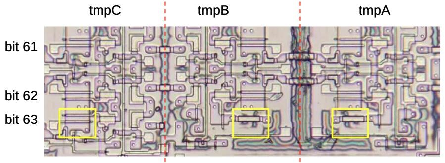
  7. The fraction datapath has three temporary registers that are almost identical but have different sizes. tmpA and tmpB hold 64 bits, but tmpC holds 68 bits (including three rounding bits and one high-order bit).

    The tmpC register has circuitry for bit 63, but tmpA and tmpB do not.

    The tmpC register has circuitry for bit 63, but tmpA and tmpB do not.

    You can see the extra tmpC bits on the die. The photo above shows the high-order bits for the three registers. For the most part, the registers are mirror images of each other. But looking at the yellow box, tmpC has a NAND gate for bit 68, which is missing from tmpB and tmpA. At the low end (not shown), tmpC has three bits for rounding that are missing from the other bits. 

  8. The patent describes the arithmetic operations in some detail. See Section III (page 13). 

Microcode inside the Intel 8087 floating-point chip: register exchange

30 May 2026 at 17:09

In 1980, Intel introduced the 8087 floating-point chip, a co-processor that made floating-point operations up to 100 times faster. This chip was highly influential, and today most processors use the floating-point standard introduced by the 8087.

The 8087 uses complicated algorithms to accurately compute functions such as square roots, tangents, and exponentials. These algorithms are implemented inside the chip in low-level code called microcode. I'm part of a group, the Opcode Collective, that is reverse-engineering this microcode. In this post, I take a close look at the microcode for one of the 8087's instructions—FXCH—and explain how the microcode works. The FXCH (Floating-point Exchange) instruction exchanges two floating-point registers. You might expect this instruction to be trivial, but there's more going on than you might expect; the microcode uses 14 micro-instructions to implement the exchange instruction.

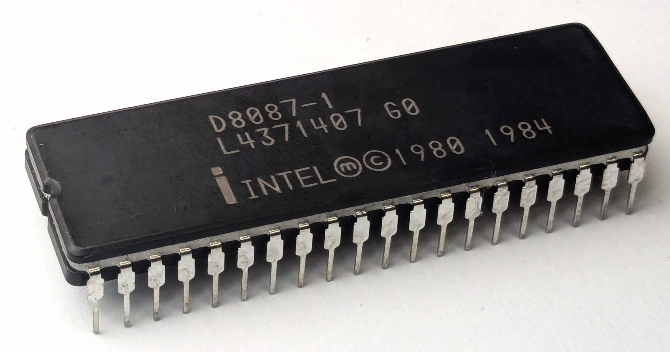
The Intel 8087 chip is packaged in a 40-pin DIP (dual in-line package).

The Intel 8087 chip is packaged in a 40-pin DIP (dual in-line package).

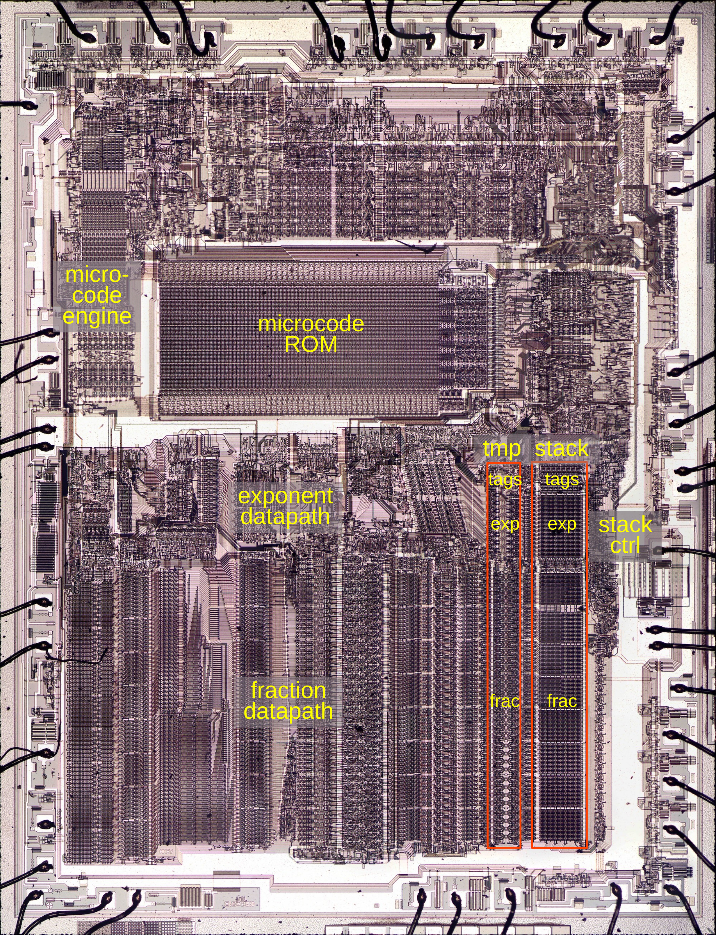
To explore the microcode, I opened up an 8087 chip and created a high-resolution image with a microscope. The large microcode ROM occupies a central position, holding the micro-instructions that control the chip. The microcode engine on the left steps through the microcode, handling jumps and subroutine calls. The bottom half of the chip is the "datapath", the circuitry that performs floating-point calculations; it is split into a 16-bit datapath for the number's exponent and a 64-bit datapath for the number's fractional part (also known as the significand).

Die of the Intel 8087 floating-point unit chip, with main functional blocks labeled. The die is 5mm×6mm.  Click for a larger image.

Die of the Intel 8087 floating-point unit chip, with main functional blocks labeled. The die is 5mm×6mm. Click for a larger image.

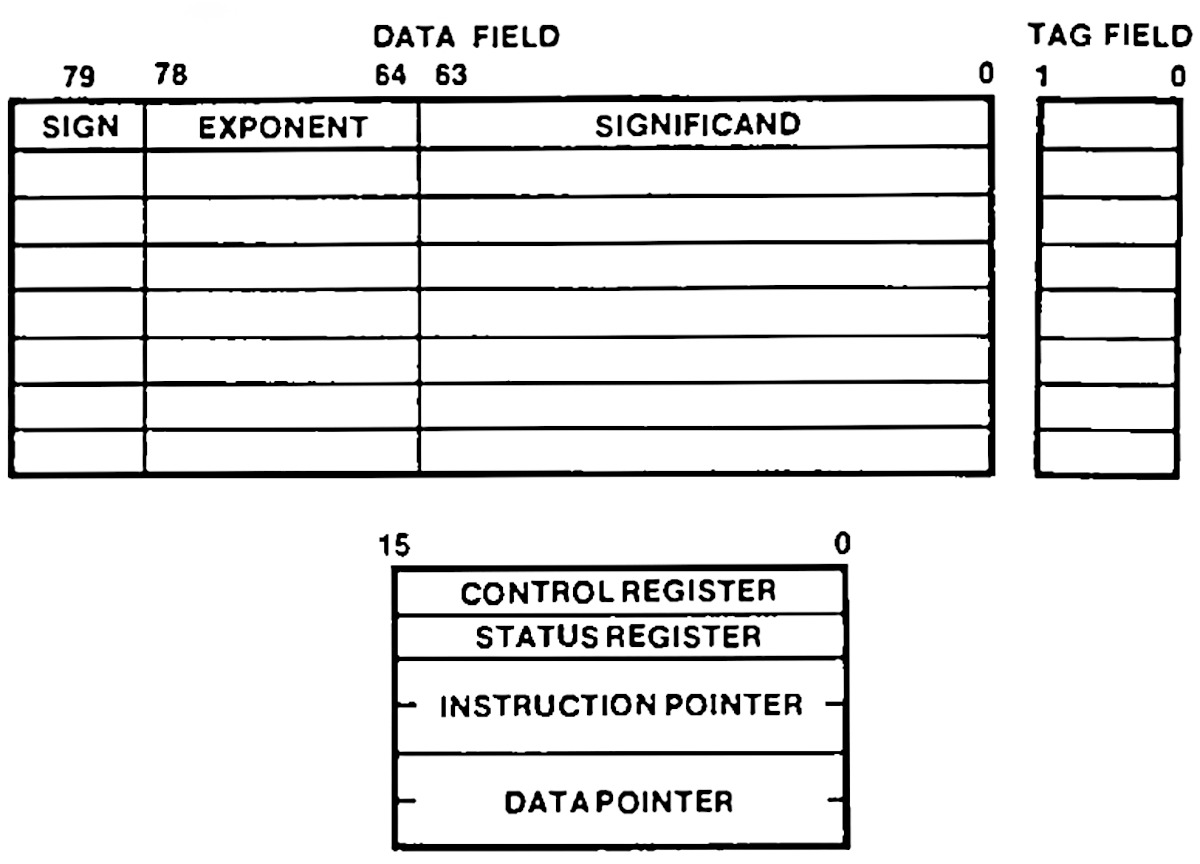
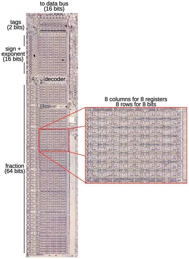
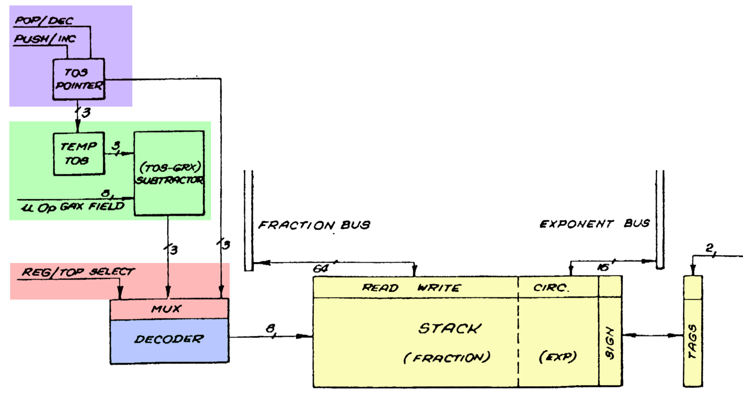
This post focuses on the temporary registers and stack registers that are highlighted in red. The chip has two temporary registers and eight stack registers, each holding a number's exponent and fraction. Each register also has two tag bits that label the type of value in the register. The stack control circuitry at the right manages the stack, keeping track of the top-of-stack position as values are pushed onto the stack or popped off the stack.

The 8087's microcode

Executing an 8087 instruction such as arctan requires hundreds of internal steps to compute the result. These steps are implemented in microcode with micro-instructions specifying each step of the algorithm. (Keep in mind the two levels of instructions: the assembly language instructions used by a programmer and the undocumented low-level micro-instructions inside the chip.) The microcode ROM holds 1648 micro-instructions, implementing the 8087's instruction set. Each micro-instruction is 16 bits long and performs a simple operation such as moving data inside the chip, adding two values, or shifting data. I'm working with the Opcode Collective to reverse-engineer the micro-instructions and fully understand the microcode (link).

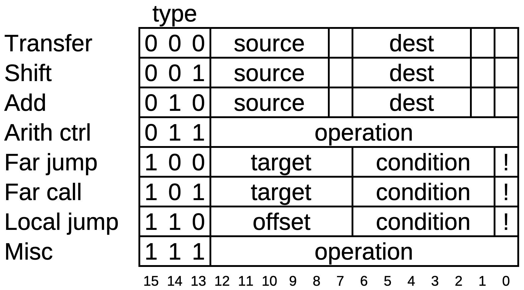
The 8087's micro-instructions are complicated, with many corner cases and ad hoc functions, but I'll provide a simplified overview. Each micro-instruction consists of 16 bits, as shown below. The first three bits specify the type of the micro-instruction, which controls the meaning of the remaining bits. The first type indicates a transfer operation, transferring data from one internal register to another. The two fields specify the source and destination for the data. The three unspecified bits are used for various special cases. Next is a shift operation, which uses the barrel shifter to shift a value left or right. The third type of micro-instruction uses the adder/subtractor. It can also be used in a loop for multiplication or division. Fourth are various arithmetic control micro-instructions that configure the adder, set rounding modes, and so forth. The far jump and far call micro-instructions perform a jump or subroutine call to a target micro-address in a fixed list. The condition field allows conditional jumps/calls based on numerous conditions, while the last bit inverts the condition. A local jump allows a conditional jump to a nearby micro-instruction. Finally, the miscellaneous micro-instructions range from returning from a subroutine or raising an exception to ending the microcode execution.

Structure of an 8087 micro-instruction.

Structure of an 8087 micro-instruction.

How values are stored inside the 8087 chip

The 8087 supports a variety of data types: floating-point numbers of various sizes, integers, and binary-coded decimal. But internally, everything is stored as an 80-bit floating-point number. A number has three parts: a 64-bit significand (the fractional part), a 15-bit exponent, and a sign bit. The chip has two separate data paths: one for the significand, and one for the exponent and sign.

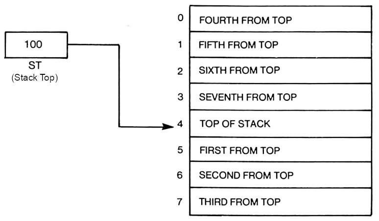
The chip has eight registers to store numbers during calculations, the top registers in the diagram below. However, the registers are organized in an unusual way: as a stack, with numbers pushed to the stack and popped from the stack. Instead of accessing, say, register #3, you might access the third register from the top of the stack, denoted ST(3); as values are pushed or popped, ST(3) changes. The stack-based architecture was intended to improve the instruction set, simplify compiler design, and make function calls more efficient, although it didn't work as well as hoped.

The register set of the 8087, as seen by the programmer. From 8086 Family Numerics Supplement.

The register set of the 8087, as seen by the programmer. From 8086 Family Numerics Supplement.

Many 8087 instructions act on the top of the stack. For instance, the square root instruction replaces the value on the top of the stack with its square root. But what if you want to take the square root of a value in the middle of the stack? The solution is the FXCH instruction, the focus of this article. This instruction exchanges the value on the top of the stack with a specified stack position, providing access to values inside the stack.

One more feature of the 8087 is important to this discussion: each value in the register stack has an associated "tag" value, labeling it as valid, special, zero, or empty. A "normal" floating-point value is tagged as valid. If the floating-point value is infinity, Not a Number, or a denormalized value, then it is tagged as special. A zero value is tagged as zero. Finally, if a register is empty (e.g., its value has been popped off the stack), the register is tagged as empty. The 8087 uses tags to optimize performance and detect errors.1 For instance, if a programmer pops too many values from the stack and tries to read a stack register that is tagged empty, the 8087 raises an "invalid operation" exception.

The eight stack registers are visible to the programmer, but the 8087 also has temporary registers that it uses internally. Two of these temporary registers are important for this article: tmpA and tmpB. Like the stack registers, each temporary register is an 80-bit register, along with two tag bits.

The FXCH microcode

In this section, I'll explain how the microcode for the FXCH exchange instruction works. This instruction exchanges the top-of-stack register with the register at a specified position in the stack. If either register is empty, the instruction will raise an "invalid operation" exception and replace the missing value(s) with the special value "Not a Number" (NaN).

The microcode for the instruction is below, consisting of 14 micro-instructions.2 The first micro-instruction is a transfer, where the source is the top of stack value ST(0) and the destination is the temporary A register. The source specification causes the 64 significand to be placed on the fraction bus, the 16-bit exponent and sign to be placed on the exponent bus, and the two tag bits to be sent to the tag circuitry. The destination tmpA causes the bus values to be stored into the temporary register. Thus, the bits in the micro-instruction cause the desired transfer to take place. The third micro-instruction is similar, but uses a register inside the stack, ST(i), with the index specified in the machine instruction.

FXCH entry point:
#0200 ST(0) -> tmpA           read top of stack
#0201 nop                     Wait a cycle
#0202 ST(i) -> tmpB           Read specified stack register
#0203 if !(tmpA or tmpB empty) jmp #0210 Jump if both registers exist
#0204 set invalid exception   Raise an invalid exception
#0205 if (unmasked) jmp #0213 If interrupt, end
#0206 if !(tmpA empty) jmp #0208 Check if tmpA is empty
#0207 NaN -> tmpA             If so, move NaN to tmpA
#0208 if !(tmpB empty) jmp #0210 Check if tmpB is empty
#0209 NaN -> tmpB             If so, move NaN to tmpB
The happy path and error path continue here:
#0210 tmpB -> ST(0)           Save tmpB to the top of stack
#0211 nop                     Wait a cycle
#0212 tmpA -> ST(i)           Save tmpA to the specified stack register
#0213 RNI                     End of routine: Run Next Instruction
#0214 nop                     Unused
#0215 nop                     Unused
#0216 nop                     Unused

Next, the relative jump at micro-address #0203 illustrates a different type of micro-instruction: the conditional jump. The micro-instruction specifies a condition, in this case, testing if either temporary register is empty. (That is, the hardware tests the tag bits associated with the temporary registers to see if either is the "empty" tag.) The micro-instruction has a bit set to invert the condition. Finally, the micro-instruction has an offset of +6, yielding the jump target #0210. The advantage of a relative offset over specifying a full micro-address is that the offset only requires six bits. (For more information on how conditions are evaluated, see my article Conditions in the Intel 8087 floating-point chip's microcode.)

If either register is empty, the next micro-instruction raises an "invalid" exception. As I'll explain in the next section, you can program the 8087 to either generate an interrupt on an exception or continue processing. The next instruction is a conditional jump that tests if the exception was "unmasked", indicating that an interrupt was generated. In this case, the microcode ends while the main 8086 processor handles the interrupt.

Assuming the interrupt was masked, the microcode now replaces empty values with the special Not a Number value, first checking tmpA and then tmpB. The source NaN causes circuitry to pull the exponent bus to all 1's and the fraction bus to all 0's, except for the top two bits. This particular bit pattern represents Not a Number.3

At micro-address #0210, the empty-register path and the normal path join up to store the temporary registers in the stack registers. This is where the actual exchange operation happens, since tmpA and tmpB are written to the opposite stack positions from where they were read. Finally, RNI (Run Next Instruction) indicates the end of the microcode routine. This stops the microcode engine and gets the 8087 ready for the next instruction.

The nop (no-operation) microcode instructions are interesting. Each pair of stack reads or writes has a nop in the middle, probably due to timing constraints on the registers. The end of the microcode routine has three nop instructions before the next microcode routine starts. These instructions appear to be wasted space in the microcode; maybe the FXCH microcode was shortened by three words during development, causing this gap.

Exceptions

The 8087 has a complicated exception system to handle a variety of problems. Exceptions fall into six categories: invalid operation, denormalized operation, zero divide, overflow, underflow, or precision. An invalid operation occurs, for instance, if you take the square root of a negative number or try to perform an operation on an empty register. An overflow exception occurs if a value is too large to be represented, while an underflow exception occurs if a value is too small. A zero divide exception happens if you divide by zero.4 A precision exception occurs if a number cannot be exactly represented as a floating-point number (which is extremely common). Finally, a denormalized exception occurs if a value is too close to zero to be represented with full accuracy.

What happens if an exception occurs? The 8087 allows the programmer to select exception behavior for each exception type. The first option is for an exception to trigger a CPU interrupt, so the software can handle the problem. For instance, the software could attempt to work around the problem, log an error, or simply terminate the program. Alternatively, the programmer can "mask" an exception. In this case, the 8087 continues the operation in a "reasonable" way. For instance, an overflowed value would be set to infinity, while an invalid value would be set to the special value: "Not a Number" (NaN). For a precision exception (e.g., 1/3), the value is rounded. The designers of the 8087 put a lot of effort into continuing after a masked exception in the best way; the manual has pages of details on all the special cases.5

Handling of exception conditions is split between microcode and hardware. For example, if the FXCH microcode detects an empty register, it executes a set invalid exception micro-instruction. This micro-instruction sets a latch indicating the invalid exception. The 8087's control register includes six mask bits, one for each type of exception, blocking interrupts for that exception type. The hardware combines the exception flip-flop signals with the mask bits in the control register and the exception flags in the status register to see if a new, unmasked interrupt has been triggered. If so, the 8087 circuitry sends an interrupt to the 8086 processor.

On the other hand, if the interrupt is masked, execution of the microcode continues. In the case of FXCH, the microcode replaces empty registers with the Not a Number value. Finally, the microcode routine ends with RNI (Run Next Instruction). This triggers many hardware activities, but the relevant one is copying the state of the exception flip-flops into the status register. This sets the exception bit if the programmer wants to check it. The exception flip-flops are cleared when the next 8087 instruction starts. Since the hardware manages the flip-flops, status register, control register, and interrupt line, the microcode can be simpler and smaller.

Extracting the microcode

The 8087's microcode ROM contains 26,368 bits, specifying 1648 16-bit micro-instructions. At the time, this was a very large ROM; in order to fit it on the die, Intel used a special type of ROM that held two bits per transistor, twice the capacity of a standard ROM. This ROM is semi-analog, using four sizes of transistors to produce four voltage levels. Comparators convert the voltage level to a pair of bits.

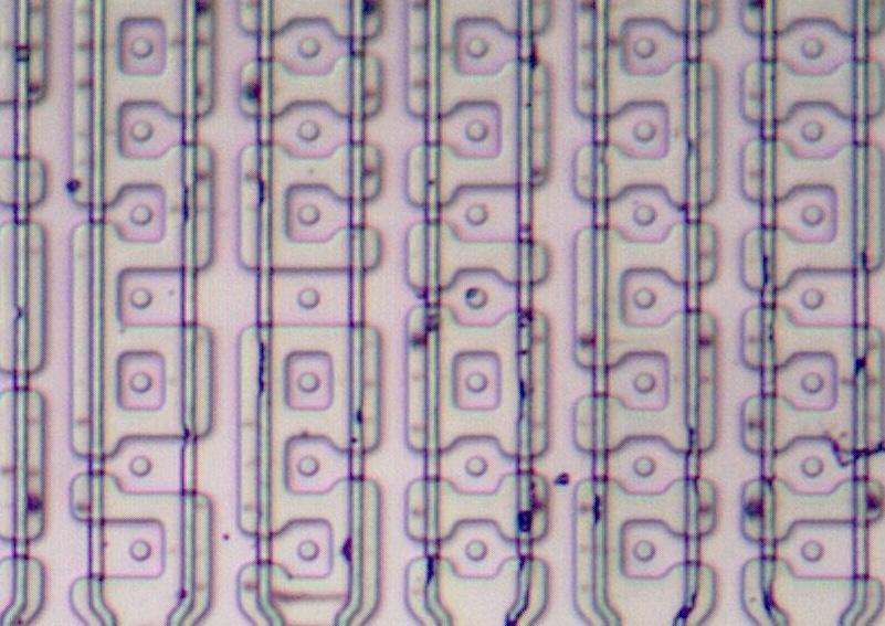
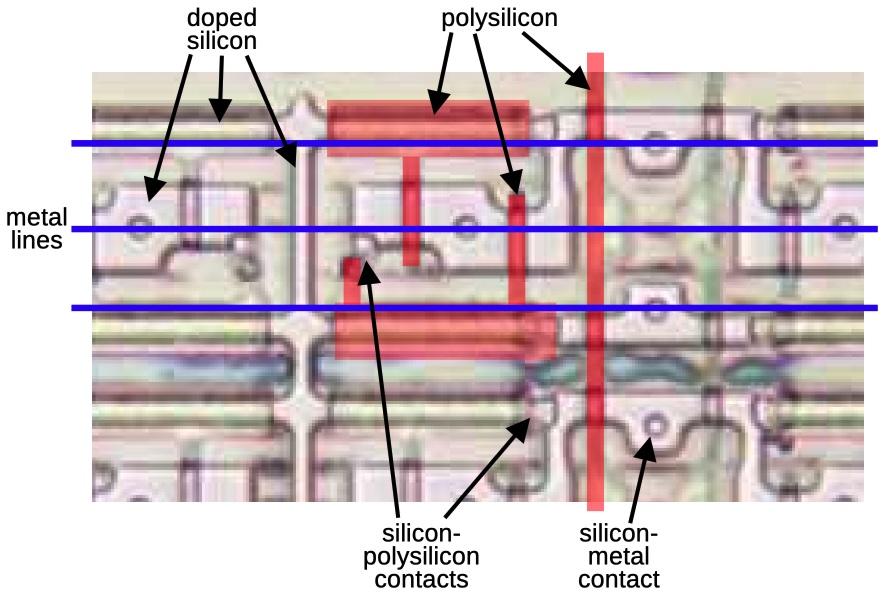
A close-up of the 8087's microcode ROM, showing 77 transistors. A transistor is formed where a vertical polysilicon line crosses a horizontal stripe of doped silicon.

A close-up of the 8087's microcode ROM, showing 77 transistors. A transistor is formed where a vertical polysilicon line crosses a horizontal stripe of doped silicon.

To extract the microcode, I took high-resolution images of the ROM after dissolving the metal layer. Gloriouscow used a neural network to categorize the size of each transistor. (You can explore the full image and transistors here.) The next step was determining how to map the transistors to bits. You might expect that the grid of transistors corresponds to the grid of microcode bits. But due to various hardware optimizations, rows and columns are shuffled and mirrored, which I sorted out by studying the circuitry. The result was the microcode, expressed as a table of 0's and 1's.

The next step was assigning meaning to the microcode. For the 8086 processor, the patent provided a lot of detail on the structure of the microcode and the hardware, but the 8087 patent didn't explain the microcode. Instead, we figured out the micro-instructions through a combination of examining the circuitry, looking for patterns in the microcode, and thinking about how instructions might be implemented.

Microcode is usually complicated, and the 8087 is worse than most. The 8087 was on the edge of what was possible at the time, so the designers resorted to special cases and hacks where necessary. For instance, some conditional jumps have side effects such as updating registers. Other instructions set flip-flops that change the behavior of later operations. We're still working to completely understand the micro-instructions at the hardware level.

I plan to continue reverse-engineering the 8087 microcode; for updates, follow me on Bluesky (@righto.com), Mastodon (@kenshirriff@oldbytes.space), or RSS. I've been working on this with the members of the "Opcode Collective", especially Smartest Blob and Gloriouscow, who converted the ROM images to microcode data and extensively analyzed the contents. See the 8087 repository on GitHub for more.

AI statement: Despite the presence of the em dash, no AI was used in the writing of this article (details).

Notes and references

  1. Tags are normally invisible to the programmer, but can be accessed through special operations. A programmer can access the 8087 tags by dumping the 8087's state to memory; the tags are stored in a 16-bit "tag word". 

  2. The raw 8087 microcode is available here, decoded by Smartest Blob. I've modified the microcode format for clarity. 

  3. The 8087 indicates a bad value with a special "Not a Number" (NaN) value. The system allows many different representations of NaN: any value with an exponent of all 1's, a nonzero significand (a zero significand indicates negative infinity), and either sign. For an invalid operation, the 8087 uses one particular NaN value, called real indefinite. For an internal 80-bit real number, this value has the top two bits of the significand set internally, and the rest zero, while the exponent bits and sign are all set. (See pages 87 (S-73) and 90 (S-76).) A 32-bit or 64-bit real uses a slightly different bit pattern for NaN; these number formats have an implied "1" bit for the significand, so only one bit of the significand is explicitly set for the real indefinite NaN. 

  4. Dividing by zero usually causes a zero divide exception, but 0 ÷ 0 causes an invalid operation exception, while infinity ÷ 0 is valid, yielding infinity. Just one reason why the microcode is so complicated. 

  5. For more information on the 8087's exceptions, see 8086 Family Numerics Supplement. The exception system is described on page 32 (S-18). The exception flags and exception masks are described on page 24 (S-10). The details of exception handling are described on page 89 (S-75). 

Instruction decoding in the Intel 8087 floating-point chip

14 February 2026 at 16:48
In the 1980s, if you wanted your IBM PC to run faster, you could buy the Intel 8087 floating-point coprocessor chip. With this chip, CAD software, spreadsheets, flight simulators, and other programs were much speedier. The 8087 chip could add, subtract, multiply, and divide, of course, but it could also compute transcendental functions such as tangent and logarithms, as well as provide constants such as π. In total, the 8087 added 62 new instructions to the computer.

But how does a PC decide if an instruction was a floating-point instruction for the 8087 or a regular instruction for the 8086 or 8088 CPU? And how does the 8087 chip interpret instructions to determine what they mean? It turns out that decoding an instruction inside the 8087 is more complicated than you might expect. The 8087 uses multiple techniques, with decoding circuitry spread across the chip. In this blog post, I'll explain how these decoding circuits work.

To reverse-engineer the 8087, I chiseled open the ceramic package of an 8087 chip and took numerous photos of the silicon die with a microscope. The complex patterns on the die are formed by its metal wiring, as well as the polysilicon and silicon underneath. The bottom half of the chip is the "datapath", the circuitry that performs calculations on 80-bit floating point values. At the left of the datapath, a constant ROM holds important constants such as π. At the right are the eight registers that the programmer uses to hold floating-point values; in an unusual design decision, these registers are arranged as a stack. Floating-point numbers cover a huge range by representing numbers with a fractional part and an exponent; the 8087 has separate circuitry to process the fractional part and the exponent.

Die of the Intel 8087 floating point unit chip, with main functional blocks labeled. The die is 5 mm×6 mm. Click this image (or any others) for a larger image.

Die of the Intel 8087 floating point unit chip, with main functional blocks labeled. The die is 5 mm×6 mm. Click this image (or any others) for a larger image.

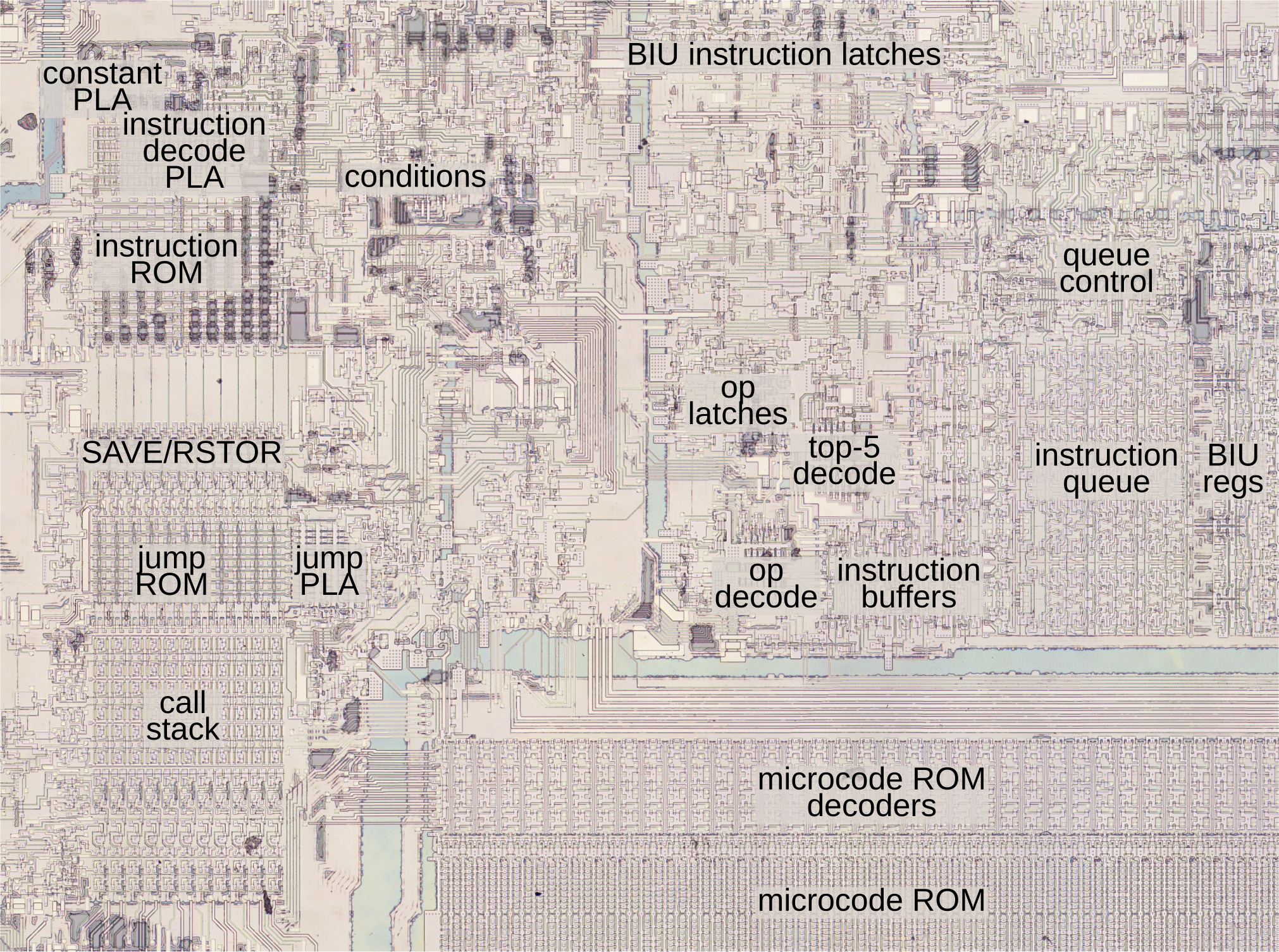
The chip's instructions are defined by the large microcode ROM in the middle.1 To execute an instruction, the 8087 decodes the instruction and the microcode engine starts executing the appropriate micro-instructions from the microcode ROM. In the upper right part of the chip, the Bus Interface Unit (BIU) communicates with the main processor and memory over the computer's bus. For the most part, the BIU and the rest of the chip operate independently, but as we will see, the BIU plays important roles in instruction decoding and execution.

Cooperation with the main 8086/8088 processor

The 8087 chip acted as a coprocessor with the main 8086 (or 8088) processor. When a floating-point instruction was encountered, the 8086 would let the 8087 floating-point chip carry out the floating-point instruction. But how do the 8086 and the 8087 determine which chip executes a particular instruction? You might expect the 8086 to tell the 8087 when it should execute an instruction, but this cooperation turns out to be more complicated.

The 8086 has eight opcodes that are assigned to the coprocessor, called ESCAPE opcodes. The 8087 determines what instruction the 8086 is executing by watching the bus, a task performed by the BIU (Bus Interface Unit).2 If the instruction is an ESCAPE, the instruction is intended for the 8087. However, there's a problem. The 8087 doesn't have any access to the 8086's registers (and vice versa), so the only way that they can exchange data is through memory. But the 8086 addresses memory through a complicated scheme involving offsest registers and segment registers. How can the 8087 determine what memory address to use when it doesn't have access to the registers?

The trick is that when an ESCAPE instruction is encountered, the 8086 processor starts executing the instruction, even though it is intended for the 8087. The 8086 computes the memory address that the instruction references and reads that memory address, but ignores the result. Meanwhile, the 8087 watches the memory bus to see what address is accessed and stores this address internally in a BIU register. When the 8087 starts executing the instruction, it uses the address from the 8086 to read and write memory. In effect, the 8087 offloads address computation to the 8086 processor.

The structure of 8087 instructions

To understand the 8087's instructions, we need to take a closer look at the structure of 8086 instructions. In particular, something called the ModR/M byte is important since all 8087 instructions use it.

The 8086 uses a complex system of opcodes with a mixture of single-byte opcodes, prefix bytes, and longer instructions. About a quarter of the opcodes use a second byte, called ModR/M, that specifies the registers and/or memory address to use through a complicated encoding. For instance, the memory address can be computed by adding the BX and SI registers, or from the BP register plus a two-byte offset. The first two bits of the ModR/M byte are the "MOD" bits. For a memory access, the MOD bits indicate how many address displacement bytes follow the ModR/M byte (0, 1, or 2), while the "R/M" bits specify how the address is computed. A MOD value of 3, however, indicates that the instruction operates on registers and does not access memory.

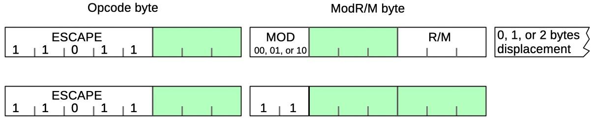
Structure of an 8087 instruction

Structure of an 8087 instruction

The diagram above shows how an 8087 instruction consists of an ESCAPE opcode, followed by a ModR/M byte. An ESCAPE opcode is indicated by the special bit pattern 11011, leaving three bits (green) available in the first byte to specify the type of 8087 instruction. As mentioned above, the ModR/M byte has two forms. The first form performs a memory access; it has MOD bits of 00,01, or 10 and the R/M bits specify how the memory address is computed. This leaves three bits (green) to specify the address. The second form operates internally, without a memory access; it has MOD bits of 11. Since the R/M bits aren't used in the second form, six bits (green) are available in the R/M byte to specify the instruction.

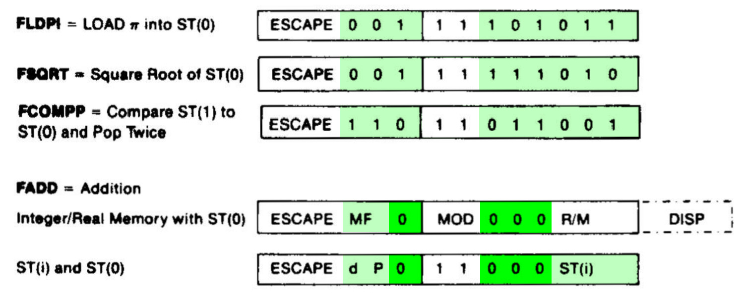
The challenge for the designers of the 8087 was to fit all the instructions into the available bits in such a way that decoding is straightforward. The diagram below shows a few 8087 instructions, illustrating how they achieve this. The first three instructions operate internally, so they have MOD bits of 11; the green bits specify the particular instruction. Addition is more complicated because it can act on memory (first format) or registers (second format), depending on the MOD bits. The four bits highlighted in bright green (0000) are the same for all ADD instructions; the subtract, multiplication, and division instructions use the same structure but have different values for the dark green bits. For instance, 0001 indicates multiplication and 0100 indicates subtraction. The other green bits (MF, d, and P) select variants of the addition instruction, changing the data format, direction, and popping the stack at the end. The last three bits select the R/M addressing mode for a memory operation, or the stack register ST(i) for a register operation.

The bit patterns for some 8087 instructions. Based on the datasheet.

The bit patterns for some 8087 instructions. Based on the datasheet.

Selecting a microcode routine

Most of the 8087's instructions are implemented in microcode, implementing each step of an instruction in low-level "micro-instructions". The 8087 chip contains a microcode engine; you can think of it as the mini-CPU that controls the 8087 by executing a microcode routine, one micro-instruction at a time. The microcode engine provides an 11-bit micro-address to the ROM, specifying the micro-instruction to execute. Normally, the microcode engine steps through the microcode sequentially, but it also supports conditional jumps and subroutine calls.

But how does the microcode engine know where to start executing the microcode for a particular machine instruction? Conceptually, you could feed the instruction opcode into a ROM that would provide the starting micro-address. However, this would be impractical since you'd need a 2048-word ROM to decode an 11-bit opcode.3 (While a 2K ROM is small nowadays, it was large at the time; the 8087's microcode ROM was a tight fit at just 1648 words.) Instead, the 8087 uses a more efficient (but complicated) instruction decode system constructed from a combination of logic gates and PLAs (Programmable Logic Arrays). This system holds 22 microcode entry points, much more practical than 2048.

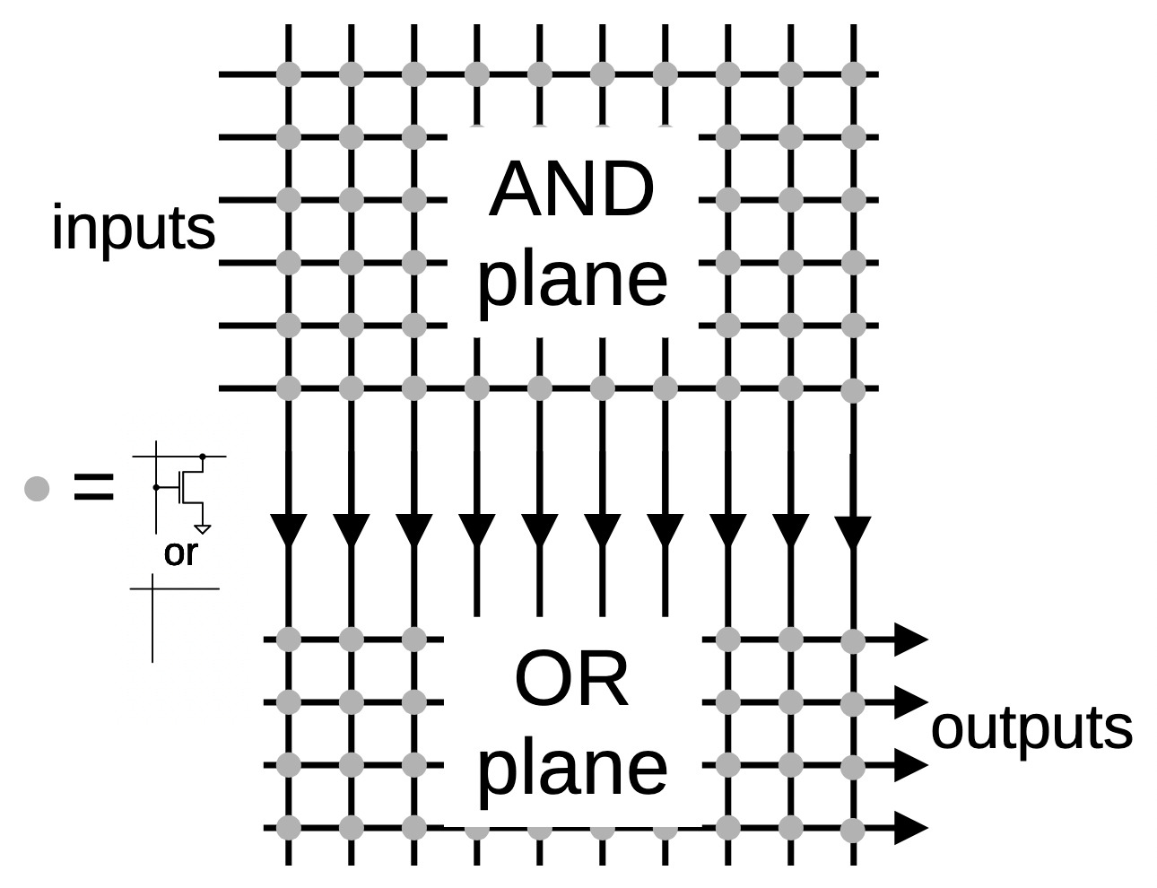
Processors often use a circuit called a PLA (Programmable Logic Array) as part of instruction decoding. The idea of a PLA is to provide a dense and flexible way of implementing arbitrary logic functions. Any Boolean logic function can be expressed as a "sum-of-products", a collection of AND terms (products) that are OR'd together (summed). A PLA has a block of circuitry called the AND plane that generates the desired sum terms. The outputs of the AND plane are fed into a second block, the OR plane, which ORs the terms together. Physically, a PLA is implemented as a grid, where each spot in the grid can either have a transistor or not. By changing the transistor pattern, the PLA implements the desired function.

A simplified diagram of a PLA.

A simplified diagram of a PLA.

A PLA can implement arbitrary logic, but in the 8087, PLAs often act as optimized ROMs.4 The AND plane matches bit patterns,5 selecting an entry from the OR plane, which holds the output values, the micro-address for each routine. The advantage of the PLA over a standard ROM is that one output column can be used for many different inputs, reducing the size.

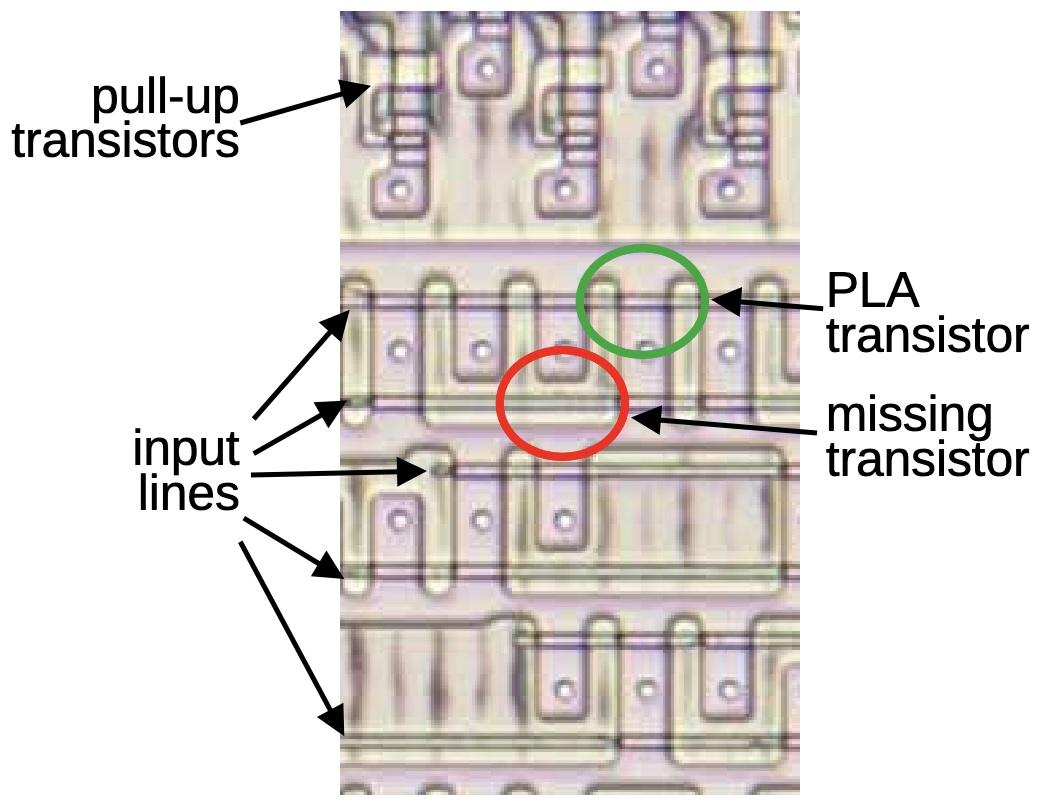
The image below shows part of the instruction decoding PLA.6 The horizontal input lines are polysilicon wires on top of the silicon. The pinkish regions are doped silicon. When polysilicon crosses doped silicon, it creates a transistor (green). Where there is a gap in the doped silicon, there is no transistor (red). (The output wires run vertically, but are not visible here; I dissolved the metal layer to show the silicon underneath.) If a polysilicon line is energized, it turns on all the transistors in its row, pulling the associated output columns to ground. (If no transistors are turned on, the pull-up transistor pulls the output high.) Thus, the pattern of doped silicon regions creates a grid of transistors in the PLA that implements the desired logic function.7

Part of the PLA for instruction decoding.

Part of the PLA for instruction decoding.

The standard way to decode instructions with a PLA is to take the instruction bits (and their complements) as inputs. The PLA can then pattern-match against bit patterns in the instruction. However, the 8087 also uses some pre-processing to reduce the size of the PLA. For instance, the MOD bits are processed to generate a signal if the bits are 0, 1, or 2 (i.e. a memory operation) and a second signal if the bits are 3 (i.e. a register operation). This allows the 0, 1, and 2 cases to be handled by a single PLA pattern. Another signal indicates that the top bits are 001 111xxxxx; this indicates that the R/M field takes part in instruction selection.8 Sometimes a PLA output is fed back in as an input, so a decoded group of instructions can be excluded from another group. These techniques all reduce the size of the PLA at the cost of some additional logic gates.

The result of the instruction decoding PLA's AND plane is 22 signals, where each signal corresponds to an instruction or group of instructions with a shared microcode entry point. The lower part of the instruction decoding PLA acts as a ROM that holds the 22 microcode entry points and provides the selected one.9

Instruction decoding inside the microcode

Many 8087 instructions share the same microcode routines. For instance, the addition, subtraction, multiplication, division, reverse subtraction, and reverse division instructions all go to the same microcode routine. This reduces the size of the microcode since these instructions share the microcode that sets up the instruction and handles the result. However, the microcode obviously needs to diverge at some point to perform the specific operation. Moreover, some arithmetic opcodes access the top of the stack, some access an arbitrary location in the stack, some access memory, and some reverse the operands, requiring different microcode actions. How does the microcode do different things for different opcodes while sharing code?

The trick is that the 8087's microcode engine supports conditional subroutine calls, returns, and jumps, based on 49 different conditions (details). In particular, fifteen conditions examine the instruction. Some conditions test specific bit patterns, such as branching if the lowest bit is set, or more complex patterns such as an opcode matching 0xx 11xxxxxx. Other conditions detect specific instructions such as FMUL. The result is that the microcode can take different paths for different instructions. For instance, a reverse subtraction or reverse division is implemented in the microcode by testing the instruction and reversing the arguments if necessary, while sharing the rest of the code.

The microcode also has a special jump target that performs a three-way jump depending on the current machine instruction that is being executed. The microcode engine has a jump ROM that holds 22 entry points for jumps or subroutine calls.10 However, a jump to target 0 uses special circuitry so it will instead jump to target 1 for a multiplication instruction, target 2 for an addition/subtraction, or target 3 for division. This special jump is implemented by gates in the upper right corner of the jump decoder.

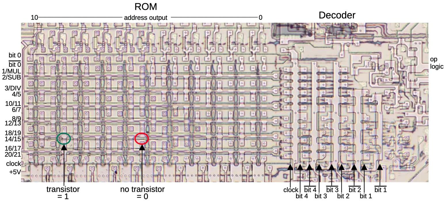
The jump decoder and ROM. Note that the rows are not in numerical order; presumably, this made the layout slightly more compact. Click this image (or any other) for a larger version.

The jump decoder and ROM. Note that the rows are not in numerical order; presumably, this made the layout slightly more compact. Click this image (or any other) for a larger version.

Hardwired instruction handling

Some of the 8087's instructions are implemented directly by hardware in the Bus Interface Unit (BIU), rather than using microcode. For example, instructions to enable or disable interrupts, or to save or restore state are implemented in hardware. The decoding for these instructions is performed by separate circuitry from the instruction decoder described above.

In the first step, a small PLA decodes the top 5 bits of the instruction. Most importantly, if these bits are 11011, it indicates an ESCAPE instruction, the start of an 8087 operation. This causes the 8087 to start interpreting the instruction and stores the opcode in a BIU register for use by the instruction decoder. A second small PLA takes the outputs from the top-5 PLA and combines them with the lower three bits. It decodes specific instruction values: D9, DB, DD, E0, E1, E2, or E3. The first three values correspond to specific ESCAPE instructions, and are recorded in latches.

The two PLAs decode the second byte in the same way. Logic gates combine the PLA outputs from the second byte with the latched values from the first byte, detecting eleven hardwired instructions.11 Some of these instructions operate directly on registers, such as clearing exceptions; the decoded instruction signal goes to the relevant register and modifies it in an ad hoc way. 12. Other hardwired instructions are more complicated, writing chip state to memory or reading chip state from memory. These instructions require multiple memory operations, controlled by the Bus Interface Unit's state machine. Each of these instructions has a flip-flop that is triggered by the decoded instruction to keep track of which instruction is active.

For the instructions that save and restore the 8087's state (FSAVE and FRSTOR), there's one more complication. These instructions are partially implemented in the BIU, which moves the relevant BIU registers to or from memory. But then, instruction processing switches to microcode, where a microcode routine saves or loads the floating-point registers. Jumping to the microcode routine is not implemented through the regular microcode jump circuitry. Instead, two hardcoded values force the microcode address to the save or restore routine.13

Constants

The 8087 has seven instructions to load floating-point constants such as π, 1, or log10(2). The 8087 has a constant ROM that holds these constants, as well as constants for transcendental operations. You might expect that the 8087 simply loads the specified constant from the constant ROM, using the instruction to select the desired constant. However, the process is much more complicated.14

Looking at the instruction decode ROM shows that different constants are implemented with different microcode routines: the constant-loading instructions FLDLG2 and FLDLN2 have one entry point; FLD1, FLD2E, FLDL2T, and FLDPI have a second entry point, and FLDZ (zero) has a third entry point. It's understandable that zero is a special case, but why are there two routines for the other constants?

The explanation is that the fraction part of each constant is stored in the constant ROM, but the exponent is stored in a separate, smaller ROM. To reduce the size of the exponent ROM, only some of the necessary exponents are stored. If a constant needs an exponent one larger than a value in the ROM, the microcode adds one to the exponent ROM value, computing the exponent on the fly.

Thus, the load-constant instructions use three separate instruction decoding mechanisms. First, the instruction decode ROM determines the appropriate microcode routine for the constant instruction, as before. Then, the constant PLA decodes the instruction to select the appropriate constant. Finally, the microcode routine tests the bottom bit of the instruction and increments the exponent if necessary.

Conclusions

To wrap up the discussion of the decoding circuitry, the diagram below shows how the different circuits are arranged on the die. This image shows the upper-right part of the die; the microcode engine is at the left and part of the ROM is at the bottom.

The upper-left portion of the 8087 die, with functional blocks labeled.

The upper-left portion of the 8087 die, with functional blocks labeled.

The 8087 doesn't have a clean architecture, but instead is full of ad hoc circuits and corner cases. The 8087's instruction decoding is an example of this. Decoding is complicated to start with due to the 8086's convoluted instruction formats and the ModR/M byte. On top of that, the 8087's instruction decoding has multiple layers: the instruction decode PLA, microcode conditional jumps that depend on the instruction, a special jump target that depends on the instruction, constants selected based on the instruction, and instructions decoded by the BIU.

The 8087 has a reason for this complicated architecture: at the time, the chip was on the edge of what was possible, so the designers needed to use whatever techniques they could to reduce the size of the chip. If implementing a corner case could shave a few transistors off the chip or make the microcode ROM slightly smaller, the corner case was worthwhile. Even so, the 8087 was barely manufacturable at first; early yield was just two working chips per silicon wafer. Despite this difficult start, a floating-point standard based on the 8087 is now part of almost every processor.

Thanks to the members of the "Opcode Collective" for their contributions, especially Smartest Blob and Gloriouscow.

For updates, follow me on Bluesky (@righto.com), Mastodon (@kenshirriff@oldbytes.space), or RSS.

Notes and references

  1. The contents of the microcode ROM are available here, partially decoded thanks to Smartest Blob. 

  2. It is difficult for the 8087 to determine what the 8086 is doing because the 8086 prefetches instructions. Thus, when an instruction is seen on the bus, the 8086 may execute it at some point in the future, or it may end up discarded.

    In order to tell what instruction is being executed, the 8087 floating-point chip internally duplicates the 8086 processor's queue. The 8087 watches the memory bus and copies any instructions that are prefetched. Since the 8087 can't tell from the bus when the 8086 starts a new instruction or when the 8086 empties the queue when jumping to a new address, the 8086 processor provides two queue status signals to the 8087. With the help of these signals, the 8087 knows exactly what the 8086 is executing.

    The 8087's instruction queue has six 8-bit registers, the same as the 8086. Surprisingly, the last two queue registers in the 8087 are tied together, so there are only five usable queue registers. My hypothesis is that since the 8087 copies the active instruction into separate registers (unlike the 8086), only five queue registers are needed. This raises the question of why the excess register wasn't removed from the die, rather than wasting valuable space.

    The 8088 processor, used in the IBM PC, has a four-byte queue instead of a six-byte queue. The 8088 is almost identical to the 8086 except it has an 8-bit memory bus instead of a 16-bit memory bus. With the narrower memory bus, prefetching is more likely to get in the way of other memory accesses, so a smaller prefetch queue was implemented.

    Knowing the queue size is essential to the 8087 floating-point chip. To indicate this, when the processor boots, a signal lets the 8087 determine if the attached processor is an 8086 or an 8088. 

  3. The relevant part of the opcode is 11 bits: the top 5 bits are always 11011 for an ESCAPE opcode, so they can be ignored during decoding. The Bus Interface Unit has a 3-bit register to hold the first byte of the instruction and an 8-bit register to hold the second byte. The BIU registers have an irregular appearance because there are 3-bit registers, 8-bit registers, and 10-bit registers (holding half of a 20-bit address). 

  4. What's the difference between a PLA and a ROM? There is a lot of overlap: a ROM can replace a PLA, while a PLA can implement a ROM. A ROM is essentially a PLA where the first stage is a binary decoder, so the ROM has a separate row for each input value. However, the first stage of a ROM can be optimized so multiple inputs share the same output value; is this a ROM or a PLA?

    The "official" difference is that in a ROM, one row is activated at a time, while in a PLA, multiple rows can be activated at once, so the output values are combined. (Thus, it is straightforward to read the values out of a ROM, but more difficult to read the values out of a PLA.)

    I consider the instruction decoding PLA to be best described as a PLA first stage with the second stage acting as a ROM. You could also call it a partially-decoded ROM, or just a PLA. Hopefully my terminology isn't too confusing. 

  5. To match a bit pattern in an instruction, the bits of the instruction are fed into the PLA, along with the complements of these bits; this allows the PLA to match against a 0 bit or a 1 bit. Each row of a PLA will match a particular bit pattern in the instruction: bits that must be 1, bits that must be 0, and bits that don't matter. If the instruction opcodes are assigned rationally, a small number of bit patterns will match all the opcodes, reducing the size of the decoder.

    I may be going too far with this analogy, but a PLA is a lot like a neural net. Each column in the AND plane is like a neuron that fires when it recognizes a particular input pattern. The OR plane is like a second layer in a neural net, combining signals from the first layer. The PLA's "weights", however, are fixed at 0 or 1, so it's not as flexible as a "real" neural net. 

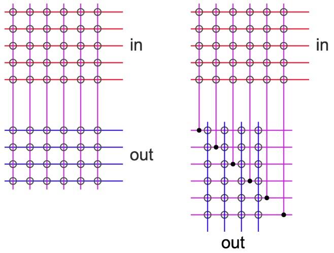
  6. The instruction decoding PLA has an unusual layout, where the second plane is rotated 90°. In a regular PLA (left), the inputs (red) go into the first plane, the perpendicular outputs from the first plane (purple) go into the second plane, and the PLA outputs (blue) exit parallel to the inputs. In the address PLA, however, the second plane is rotated 90°, so the outputs are perpendicular to the inputs. This approach requires additional wiring (horizontal purple lines), but presumably, this layout worked better in the 8087 since the outputs are lined up with the rest of the microcode engine.

    Conceptual diagram of a regular PLA on the left and a rotated PLA on the right.

    Conceptual diagram of a regular PLA on the left and a rotated PLA on the right.


  7. To describe the implementation of a PLA in more detail, the transistors in each row of the AND plane form a NOR gate, since if any transistor is turned on, it pulls the output low. Likewise, the transistors in each column of the OR plane form a NOR gate. So why is the PLA described as having an AND plane and an OR plane, rather than two NOR planes? By using De Morgan's law, you can treat the NOR-NOR Boolean equations as equivalent to AND-OR Boolean equations (with the inputs and outputs inverted). It's usually much easier to understand the logic as AND terms OR'd together.

    The converse question is why don't they build the PLA from AND and OR gates instead of NOR gates? The reason is that AND and OR gates are harder to build with NMOS transistors, since you need to add explicit inverter circuits. Moreover, NMOS NOR gates are typically faster than NAND gates because the transistors are in parallel. (CMOS is the opposite; NAND gates are faster because the weaker PMOS transistors are in parallel.) 

  8. The 8087's opcodes can be organized into tables, showing the underlying structure. (In each table, the row (Y) coordinate is the bottom 3 bits of the first byte and the column (X) coordinate is the 3 bits after the MOD bits in the second byte.)

    Memory operations use the following encoding with MOD = 0, 1, or 2. Each box represents 8 different addressing modes.

      0 1 2 3 4 5 6 7
    0 FADD FMUL FCOM FCOMP FSUB FSUBR FDIV FDIVR
    1 FLD   FST FSTP FLDENV FLDCW FSTENV FSTCW
    2 FIADD FIMUL FICOM FICOMP FISUB FISUBR FIDIV FIDIVR
    3 FILD   FIST FISTP   FLD   FSTP
    4 FADD FMUL FCOM FCOMP FSUB FSUBR FDIV FDIVR
    5 FLD   FST FSTP FRSTOR   FSAVE FSTSW
    6 FIADD FIMUL FICOM FICOMP FISUB FISUBR FIDIV FIDIVR
    7 FILD   FIST FISTP FBLD FILD FBSTP FISTP

    The important point is that the instruction encoding has a lot of regularity, making the decoding process easier. For instance, the basic arithmetic operations (FADD through FDIVR) are repeated on alternating rows. However, the table also has significant irregularities, which complicate the decoding process.

    The register operations (MOD = 3) have a related layout, but there are even more irregularities.

      0 1 2 3 4 5 6 7
    0 FADD FMUL FCOM FCOMP FSUB FSUBR FDIV FDIVR
    1 FLD FXCH FNOP   misc1 misc2 misc3 misc4
    2                
    3         misc5      
    4 FADD FMUL     FSUB FSUBR FDIV FDIVR
    5 FFREE   FST FSTP        
    6 FADDP FMULP   FCOMPP FSUBP FSUBRP FDIVP FDIVRP
    7                

    In most cases, each box indicates 8 different values for the stack register, but there are exceptions. The NOP and FCOMPP instructions each have a single opcode, "wasting" the rest of the box.

    Five of the boxes in the table encode multiple instructions instead of the register number. The first four (red) are miscellaneous instructions handled by the decoding PLA:
    misc1 = FCHS, FABS, FTST, FXAM
    misc2 = FLD1, FLDL2T, FLDL2E, FLDPI, FLDLG2, FLDLN2, FLDZ (the constant-loading instructions)
    misc3 = F2XM1, FYL2X, FPTAN, FPATAN, FXTRACT, FDECSTP, FINCSTP
    misc4 = FPREM, FYL2XP1, FSQRT, FRNDINT, FSCALE

    The last miscellaneous box (yellow) holds instructions that are handled by the BIU.
    misc5 = FENI, FDISI, FCLEX, FINIT

    Curiously, the 8087's opcodes (like the 8086's) make much more sense in octal than in hexadecimal. In octal, an 8087 opcode is simply 33Y MXR, where X and Y are the table coordinates above, M is the MOD value (0, 1, 2, or 3), and R is the R/M field or the stack register number. 

  9. The 22 outputs from the instruction decoder PLA correspond to the following groups of instructions, activating one row of ROM and producing the corresponding microcode address. From this table, you can see which instructions are grouped together in the microcode.

     0 #0200 FXCH
     1 #0597 FSTP (BCD)
     2 #0808 FCOM FCOMP FCOMPP
     3 #1008 FLDLG2 FLDLN2
     4 #1527 FSQRT
     5 #1586 FPREM
     6 #1138 FPATAN
     7 #1039 FPTAN
     8 #0900 F2XM1
     9 #1020 FLDZ
    10 #0710 FRNDINT
    11 #1463 FDECSTP FINCSTP
    12 #0812 FTST
    13 #0892 FABS FCHS
    14 #0065 FFREE FLD
    15 #0217 FNOP FST FSTP (not BCD)
    16 #0001 FADD FDIV FDIVR FMUL FSUB FSUBR
    17 #0748 FSCALE
    18 #1028 FXTRACT
    19 #1257 FYL2X FYL2XP1
    20 #1003 FLD1 FLDL2E FLDL2T FLDPI
    21 #1468 FXAM
    
     
  10. The instruction decoding PLA has 22 entries, and the jump table also has 22 entries. It's a coincidence that these values are the same.

    An entry in the jump table ROM is selected by five bits of the micro-instruction. The ROM is structured with two 11-bit words per row, interleaved. (It's also a coincidence that there are 22 bits.) The upper four bits of the jump number select a row in the ROM, while the bottom bit selects one of the two rows.

    This implementation is modified for target 0, the three-way jump. The first ROM row is selected for target 0 if the current instruction is multiplication, or for target 1. The second row is selected for target 0 if the current instruction is addition or subtraction, or for target 2. The third row is selected for target 0 if the current instruction is division, or for target 3. Thus, target 0 ends up selecting rows 1, 2, or 3. However, remember that there are two words per row, selected by the low bit of the target number. The problem is that target 0 with multiplication will access the left word of row 1, while target 1 will access the right word of row 1, but both should provide the same address. The solution is that rows 1, 2, and 3 have the same address stored twice in the row, so these rows each "waste" a value.

    For reference, the contents of the jump table are:

     0: Jumps to target 1 for FMUL, 2 for FADD/FSUB/FSUBR, 3 for FDIV/FDIVR
     1: #0359
     2: #0232
     3: #0410
     4: #0083
     5: #1484
     6: #0122
     7: #0173
     8: #0439
     9: #0655
    10: #0534
    11: #0299
    12: #1572
    13: #1446
    14: #0859
    15: #0396
    16: #0318
    17: #0380
    18: #0779
    19: #0868
    20: #0522
    21: #0801
    
     
  11. Eleven instructions are implemented in the BIU hardware. Four of these are relatively simple, setting or clearing bits: FINIT (initialize), FENI (enable interrupts), FDISI (disable interrupts), and FCLEX (clear exceptions). Six of these are more complicated, storing state to memory or loading state from memory: FLDCW (load control word), FSTCW (store control word), FSTSW (store status word), FSTENV (store environment), FLDENV (load environment), FSAVE (save state), and FRSTOR (restore state). As explained elsewhere, the last two instructions are partially implemented in microcode. 

  12. Even a seemingly trivial instruction uses more circuitry than you might expect. For instance, after the FCLEX (clear exception) instruction is decoded, the signal goes through nine gates before it clears the exception bits in the status register. Along the way, it goes through a flip-flop to synchronize the timing, a gate to combine it with the reset signal, and various inverters and drivers. Even though these instructions seem like they should complete immediately, they typically take 5 clock cycles due to overhead in the 8087. 

  13. I'll give more details here on the circuit that jumps to the save or restore microcode. The BIU sends two signals to the microcode engine, one to jump to the save code and one to jump to the restore code. These signals are buffered and delayed by a capacitor, probably to adjust the timing of the signal.

    In the microcode engine, there are two hardcoded constants for the routines, just above the jump table; the BIU signal causes the appropriate constant to go onto the micro-address lines. Each bit in the address has a pull-up transistor to +5V or a pull-down transistor to ground. This approach is somewhat inefficient since it requires two transistor sites per bit. In comparison, the jump address ROM and the instruction address ROM use one transistor site per bit. (As in a PLA, each transistor is present or absent as needed, so the number of physical transistors is less than the number of transistor sites.)

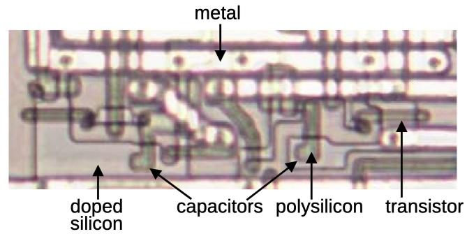
    Two capacitors in the 8087. This photo shows the metal layer with the silicon and polysilicon underneath.

    Two capacitors in the 8087. This photo shows the metal layer with the silicon and polysilicon underneath.

    Since capacitors are somewhat unusual in NMOS circuits, I'll show them in the photo above. If a polysilicon line crosses over doped silicon, it creates a transistor. However, if a polysilicon region sits on top of the doped silicon without crossing it, it forms a capacitor instead. (The capacitance exists for a transistor, too, but the gate capacitance is generally unwanted.) 

  14. The documentation provides a hint that the microcode to load constants is complicated. Specifically, the documentation shows that different constants take different amounts of time to load. For instance, log2(e) takes 18 cycles while log2(10) takes 19 cycles and log10(2) takes 21 cycles. You'd expect that pre-computed constants would all take the same time, so the varying times show that more is happening behind the scenes. 

Conditions in the Intel 8087 floating-point chip's microcode

30 December 2025 at 18:00

In the 1980s, if you wanted your computer to do floating-point calculations faster, you could buy the Intel 8087 floating-point coprocessor chip. Plugging it into your IBM PC would make operations up to 100 times faster, a big boost for spreadsheets and other number-crunching applications. The 8087 uses complicated algorithms to compute trigonometric, logarithmic, and exponential functions. These algorithms are implemented inside the chip in microcode. I'm part of a group that is reverse-engineering this microcode. In this post, I examine the 49 types of conditional tests that the 8087's microcode uses inside its algorithms. Some conditions are simple, such as checking if a number is zero or negative, while others are specialized, such as determining what direction to round a number.

To explore the 8087's circuitry, I opened up an 8087 chip and took numerous photos of the silicon die with a microscope. Around the edges of the die, you can see the hair-thin bond wires that connect the chip to its 40 external pins. The complex patterns on the die are formed by its metal wiring, as well as the polysilicon and silicon underneath. The bottom half of the chip is the "datapath", the circuitry that performs calculations on 80-bit floating point values. At the left of the datapath, a constant ROM holds important constants such as π. At the right are the eight registers that the programmer uses to hold floating-point values; in an unusual design decision, these registers are arranged as a stack.

Die of the Intel 8087 floating point unit chip, with main functional blocks labeled. The die is 5mm×6mm.  Click for a larger image.

Die of the Intel 8087 floating point unit chip, with main functional blocks labeled. The die is 5mm×6mm. Click for a larger image.

The chip's instructions are defined by the large microcode ROM in the middle. To execute a floating-point instruction, the 8087 decodes the instruction and the microcode engine starts executing the appropriate micro-instructions from the microcode ROM. The microcode decode circuitry to the right of the ROM generates the appropriate control signals from each micro-instruction.1 The bus registers and control circuitry handle interactions with the main 8086 processor and the rest of the system.

The 8087's microcode

Executing an 8087 instruction such as arctan requires hundreds of internal steps to compute the result. These steps are implemented in microcode with micro-instructions specifying each step of the algorithm. (Keep in mind the difference between the assembly language instructions used by a programmer and the undocumented low-level micro-instructions used internally by the chip.) The microcode ROM holds 1648 micro-instructions, implementing the 8087's instruction set. Each micro-instruction is 16 bits long and performs a simple operation such as moving data inside the chip, adding two values, or shifting data. I'm working with the "Opcode Collective" to reverse engineer the micro-instructions and fully understand the microcode (link).

The microcode engine (below) controls the execution of micro-instructions, acting as the mini-CPU inside the 8087. Specifically, it generates an 11-bit micro-address, the address of a micro-instruction in the ROM. The microcode engine implements jumps, subroutine calls, and returns within the microcode. These jumps, subroutine calls, and returns are all conditional; the microcode engine will either perform the operation or skip it, depending on the value of a specified condition.

The microcode engine. In this image, the metal is removed, showing the underlying silicon and polysilicon.

The microcode engine. In this image, the metal is removed, showing the underlying silicon and polysilicon.

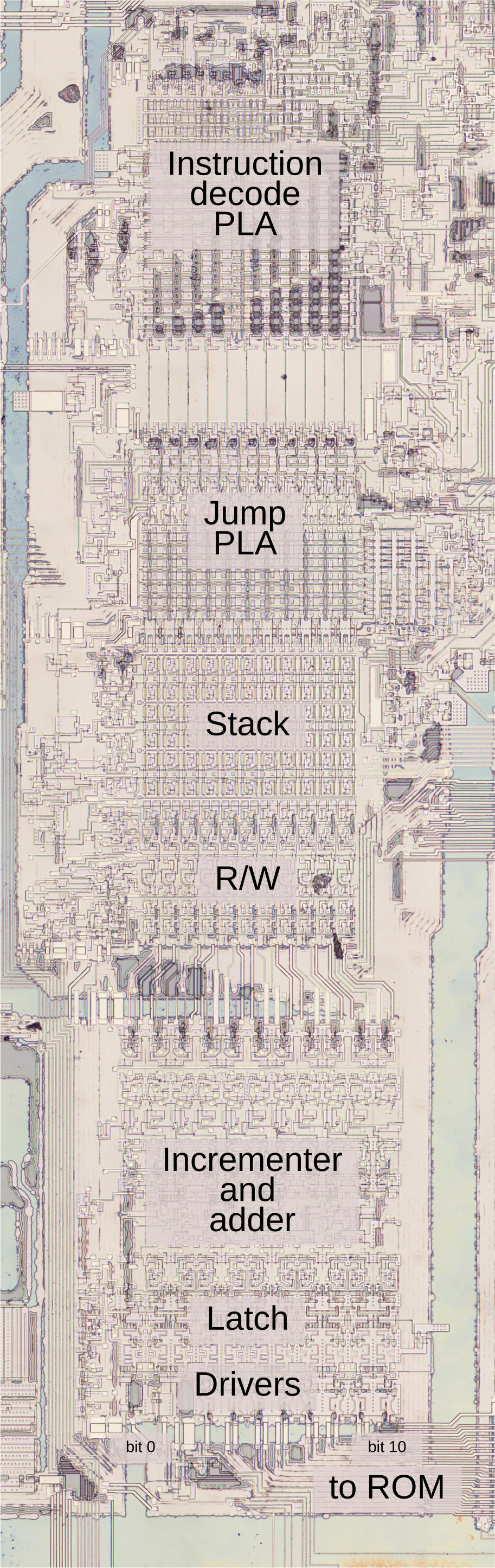
I'll write more about the microcode engine later, but I'll give an overview here. At the top, the Instruction Decode PLA2 decodes an 8087 instruction to determine the starting address in microcode. Below that, the Jump PLA holds microcode addresses for jumps and subroutine calls. Below this, six 11-bit registers implement the microcode stack, allowing six levels of subroutine calls inside the microcode. (Note that this stack is completely different from the 8087's register stack that holds eight floating-point values.) The stack registers have associated read/write circuitry. The incrementer adds one to the micro-address to step through the code. The engine also implements relative jumps, using an adder to add an offset to the current location. At the bottom, the address latch and drivers boost the 11-bit address output and send it to the microcode ROM.

Selecting a condition

A micro-instruction can say "jump ahead 5 micro-instructions if a register is zero" and the microcode engine will either perform the jump or ignore it, based on the register value. In the circuitry, the condition causes the microcode engine to either perform the jump or block the jump. But how does the hardware select one condition out of the large set of conditions?

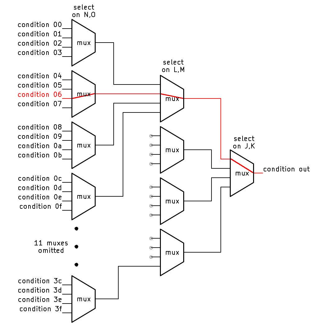
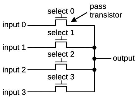
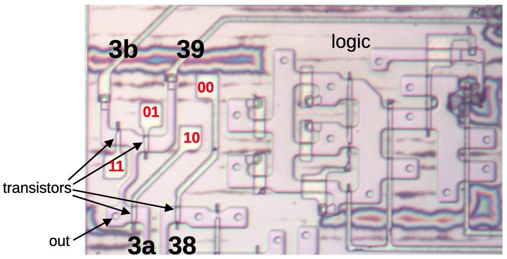
Six bits of the micro-instruction can specify one of 64 conditions. A circuit similar to the idealized diagram below selects the specified condition. The key component is a multiplexer, represented by a trapezoid below. A multiplexer is a simple circuit that selects one of its four inputs. By arranging multiplexers in a tree, one of the 64 conditions on the left is selected and becomes the output, passed to the microcode engine.

A tree of multiplexers selects one of the conditions. This diagram is simplified.

A tree of multiplexers selects one of the conditions. This diagram is simplified.

For example, if bits J and K of the microcode are 00, the rightmost multiplexer will select the first input. If bits LM are 01, the middle multiplexer will select the second input, and if bits NO are 10, the left multiplexer will select its third input. The result is that condition 06 will pass through the tree and become the output.3 By changing the bits that control the multiplexers, any of the inputs can be used. (We've arbitrarily given the 16 microcode bits the letter names A through P.)

Physically, the conditions come from locations scattered across the die. For instance, conditions involving the opcode come from the instruction decoding part of the chip, while conditions involving a register are evaluated next to the register. It would be inefficient to run 64 wires for all the conditions to the microcode engine. The tree-based approach reduces the wiring since the "leaf" multiplexers can be located near the associated condition circuitry. Thus, only one wire needs to travel a long distance rather than multiple wires. In other words, the condition selection circuitry is distributed across the chip instead of being implemented as a centralized module.

Because the conditions don't always fall into groups of four, the actual implementation is slightly different from the idealized diagram above. In particular, the top-level multiplexer has five inputs, rather than four.4 Other multiplexers don't use all four inputs. This provides a better match between the physical locations of the condition circuits and the multiplexers. In total, 49 of the possible 64 conditions are implemented in the 8087.

The circuit that selects one of the four conditions is called a multiplexer. It is constructed from pass transistors, transistors that are configured to either pass a signal through or block it. To operate the multiplexer, one of the select lines is energized, turning on the corresponding pass transistor. This allows the selected input to pass through the transistor to the output, while the other inputs are blocked.

A 4-1 multiplexer, constructed from four pass transistors.

A 4-1 multiplexer, constructed from four pass transistors.

The diagram below shows how a multiplexer appears on the die. The pinkish regions are doped silicon. The white lines are polysilicon wires. When polysilicon crosses over doped silicon, a transistor is formed. On the left is a four-way multiplexer, constructed from four pass transistors. It takes inputs (black) for four conditions, numbered 38, 39, 3a, and 3b. There are four control signals (red) corresponding to the four combinations of bits N and O. One of the inputs will pass through a transistor to the output, selected by the active control signal. The right half contains the logic (four NOR gates and two inverters) to generate the control signals from the microcode bits. (Metal lines run horizontally from the logic to the control signal contacts, but I dissolved the metal for this photo.) Each multiplexer in the 8087 has a completely different layout, manually optimized based on the location of the signals and surrounding circuitry. Although the circuit for a multiplexer is regular (four transistors in parallel), the physical layout looks somewhat chaotic.

Multiplexers as they appear on the die. The metal layer has been removed to show the polysilicon and silicon. The "tie-die" patterns are due to thin-film effects where the oxide layer wasn't completely removed.

Multiplexers as they appear on the die. The metal layer has been removed to show the polysilicon and silicon. The "tie-die" patterns are due to thin-film effects where the oxide layer wasn't completely removed.

The 8087 uses pass transistors for many circuits, not just multiplexers. Circuits with pass transistors are different from regular logic gates because the pass transistors provide no amplification. Instead, signals get weaker as they go through pass transistors. To solve this problem, inverters or buffers are inserted into the condition tree to boost signals; they are omitted from the diagram above.

The conditions

Of the 8087's 49 different conditions, some are widely used in the microcode, while others are designed for a specific purpose and are only used once. The full set of conditions is described in a footnote7 but I'll give some highlights here.

Fifteen conditions examine the bits of the current instruction's opcode. This allows one microcode routine to handle a group of similar instructions and then change behavior based on the specific instruction. For example, conditions test if the instruction is multiplication, if the instruction is an FILD/FIST (integer load or store), or if the bottom bit of the opcode is set.5

The 8087 has three temporary registers—tmpA, tmpB, and tmpC—that hold values during computation. Various conditions examine the values in the tmpA and tmpB registers.6 In particular, the 8087 uses an interesting way to store numbers internally: each 80-bit floating-point value also has two "tag" bits. These bits are mostly invisible to the programmer and can be thought of as metadata. The tag bits indicate if a register is empty, contains zero, contains a "normal" number, or contains a special value such as NaN (Not a Number) or infinity. The 8087 uses the tag bits to optimize operations. The tags also detect stack overflow (storing to a non-empty stack register) or stack underflow (reading from an empty stack register).

Other conditions are highly specialized. For instance, one condition looks at the rounding mode setting and the sign of the value to determine if the value should be rounded up or down. Other conditions deal with exceptions such as numbers that are too small (i.e. denormalized) or numbers that lose precision. Another condition tests if two values have the same sign or not. Yet another condition tests if two values have the same sign or not, but inverts the result if the current instruction is subtraction. The simplest condition is simply "true", allowing an unconditional branch.

For flexibility, conditions can be "flipped", either jumping if the condition is true or jumping if the condition is false. This is controlled by bit P of the microcode. In the circuitry, this is implemented by a gate that XORs the P bit with the condition. The result is that the state of the condition is flipped if bit P is set.

For a concrete example of how conditions are used, consider the microcode routine that implements FCHS and FABS, the instructions to change the sign and compute the absolute value, respectively. These operations are almost the same (toggling the sign bit versus clearing the sign bit), so the same microcode routine handles both instructions, with a jump instruction to handle the difference. The FABS and FCHS instructions were designed with identical opcodes, except that the bottom bit is set for FABS. Thus, the microcode routine uses a condition that tests the bottom bit, allowing the routine to branch and change its behavior for FABS vs FCHS.

Looking at the relevant micro-instruction, it has the hex value 0xc094, or in binary 110 000001 001010 0. The first three bits (ABC=110) specify the relative jump operation (100 would jump to a fixed target and 101 would perform a subroutine call.) Bits D through I (000010) indicate the amount of the jump (+`). Bits J through O (001010, hex 0a) specify the condition to test, in this case, the last bit of the instruction opcode. The final bit (P) would toggle the condition if set, (i.e. jump if false). Thus, for FABS, the jump instruction will jump ahead one micro-instruction. This has the effect of skipping the next micro-instruction, which sets the appropriate sign bit for FCHS.

Conclusions

The 8087 performs floating-point operations much faster than the 8086 by using special hardware, optimized for floating-point. The condition code circuitry is one example of this: the 8087 can test a complicated condition in a single operation. However, these complicated conditions make it much harder to understand the microcode. But by a combination of examining the circuitry and looking at the micocode, we're making progress. Thanks to the members of the "Opcode Collective" for their hard work, especially Smartest Blob and Gloriouscow.

For updates, follow me on Bluesky (@righto.com), Mastodon (@kenshirriff@oldbytes.space), or RSS.

Notes and references

  1. The section of the die that I've labeled "Microcode decode" performs some of the microcode decoding, but large parts of the decoding are scattered across the chip, close to the circuitry that needs the signals. This makes reverse-engineering the microcode much more difficult. I thought that understanding the microcode would be straightforward, just examining a block of decode circuitry. But this project turned out to be much more complicated and I need to reverse-engineer the entire chip. 

  2. A PLA is a "Programmable Logic Array". It is a technique to implement logic functions with grids of transistors. A PLA can be used as a compressed ROM, holding data in a more compact representation. (Saving space was very important in chips of this era.) In the 8087, PLAs are used to hold tables of microcode addresses. 

  3. Note that the multiplexer circuit selects the condition corresponding to the binary value of the bits. In the example, bits 000110 (0x06) select condition 06. 

  4. The five top-level multiplexer inputs correspond to bit patterns 00, 011, 10, 110, and 111. That is, two inputs depend on bits J and K, while three inputs depend on bits J, K, and L. The bit pattern 010 is unused, corresponding to conditions 0x10 through 0x17, which aren't implemented. 

  5. The 8087 acts as a co-processor with the 8086 processor. The 8086 instruction set is designed so instructions with a special "ESCAPE" sequence in the top 5 bits are processed by the co-processor, in this case the 8087. Thus, the 8087 receives a 16-bit instruction, but only the bottom 11 bits are usable. For a memory operation, the second byte of the instruction is an 8086-style ModR/M byte. For instructions that don't access memory, the second byte specifies more of the instruction and sometimes specifies the stack register to use for the instruction.

    The relevance of this is that the 8087's microcode engine uses the 11 bits of the instruction to determine which microcode routine to execute. The microcode also uses various condition codes to change behavior depending on different bits of the instruction. 

  6. There is a complication with the tmpA and tmpB registers: they can be swapped with the micro-instruction "ABC.EF". The motivation behind this is that if you have two arguments, you can use a micro-subroutine to load an argument into tmpA, swap the registers, and then use the same subroutine to load the second argument into tmpA. The result is that the two arguments end up in tmpB and tmpA without any special coding in the subroutine.

    The implementation doesn't physically swap the registers, but renames them internally, which is much more efficient. A flip-flop is toggled every time the registers are swapped. If the flip-flop is set, a request goes to one register, while if the flip-flop is clear, a request goes to the other register. (Many processors use the same trick. For instance, the Intel 8080 has an instruction to exchange the DE and HL registers. The Z80 has an instruction to swap register banks. In both cases, a flip-flop renames the registers, so the data doesn't need to move.) 

  7. The table below is the real meat of this post, the result of much circuit analysis. These details probably aren't interesting to most people, so I've relegated the table to a footnote. Descriptions in italics are provided by Smartest Blob based on examination of the microcode. Grayed-out lines are unused conditions.

    The table has five sections, corresponding to the 5 inputs to the top-level condition multiplexer. These inputs come from different parts of the chip, so the sections correspond to different categories of conditions.

    The first section consists of instruction parsing, with circuitry near the microcode engine. The description shows the 11-bit opcode pattern that triggers the condition, with 0 bits and 1 bits as specified, and X indicating a "don't care" bit that can be 0 or 1. Where simpler, I list the relevant instructions instead.

    The next section indicates conditions on the exponent. I am still investigating these conditions, so the descriptions are incomplete. The third section is conditions on the temporary registers or conditions related to the control register. These circuits are to the right of the microcode ROM.

    Conditions in the fourth section examine the floating-point bus, with circuitry near the bottom of the chip. Conditions 34 and 35 use a special 16-bit bidirectional shift register, at the far right of the chip. The top bit from the floating-point bus is shifted in. Maybe this shift register is used for CORDIC calculations? The conditions in the final block are miscellaneous, including the always-true condition 3e, which is used for unconditional jumps.

    Cond.Description
    00not XXX 11XXXXXX
    011XX 11XXXXXX
    020XX 11XXXXXX
    03X0X XXXXXXXX
    04not cond 07 or 1XX XXXXXXXX
    05not FLD/FSTP temp-real or BCD
    06110 xxxxxxxx or 111 xx0xxxxx
    07FLD/FSTP temp-real
    08FBLD/FBSTP
    09
    0aXXX XXXXXXX1
    0bXXX XXXX1XXX
    0cFMUL
    0dFDIV FDIVR
    0eFADD FCOM FCOMP FCOMPP FDIV FDIVR FFREE FLD FMUL FST FSTP FSUB FSUBR FXCH
    0fFCOM FCOMP FCOMPP FTST
    10
    11
    12
    13
    14
    15
    16
    17
    18exponent condition
    19exponent condition
    1aexponent condition
    1bexponent condition
    1cexponent condition
    1dexponent condition
    1eeight exponent zero bits
    1fexponent condition
    20tmpA tag ZERO
    21tmpA tag SPECIAL
    22tmpA tag VALID
    23stack overflow
    24tmpB tag ZERO
    25tmpB tag SPECIAL
    26tmpB tag VALID
    27st(i) doesn't exist (A)?
    28tmpA sign
    29tmpB top bit
    2atmpA zero
    2btmpA top bit
    2cControl Reg bit 12: infinity control
    2dround up/down
    2eunmasked interrupt
    2fDE (denormalized) interrupt
    30top reg bit
    31
    32reg bit 64
    33reg bit 63
    34Shifted top bits, all zero
    35Shifted top bits, one out
    36
    37
    38const latch zero
    39tmpA vs tmpB sign, flipped for subtraction
    3aprecision exception
    3btmpA vs tmpB sign
    3c
    3d
    3eunconditional
    3f

    This table is under development and undoubtedly has errors. 

The stack circuitry of the Intel 8087 floating point chip, reverse-engineered

9 December 2025 at 17:54

Early microprocessors were very slow when operating with floating-point numbers. But in 1980, Intel introduced the 8087 floating-point coprocessor, performing floating-point operations up to 100 times faster. This was a huge benefit for IBM PC applications such as AutoCAD, spreadsheets, and flight simulators. The 8087 was so effective that today's computers still use a floating-point system based on the 8087.1

The 8087 was an extremely complex chip for its time, containing somewhere between 40,000 and 75,000 transistors, depending on the source.2 To explore how the 8087 works, I opened up a chip and took numerous photos of the silicon die with a microscope. Around the edges of the die, you can see the hair-thin bond wires that connect the chip to its 40 external pins. The complex patterns on the die are formed by its metal wiring, as well as the polysilicon and silicon underneath. The bottom half of the chip is the "datapath", the circuitry that performs calculations on 80-bit floating point values. At the left of the datapath, a constant ROM holds important constants such as π. At the right are the eight registers that form the stack, along with the stack control circuitry.

Die of the Intel 8087 floating point unit chip, with main functional blocks labeled. The die is 5mm×6mm.  Click for a larger image.

Die of the Intel 8087 floating point unit chip, with main functional blocks labeled. The die is 5mm×6mm. Click for a larger image.

The chip's instructions are defined by the large microcode ROM in the middle. This ROM is very unusual; it is semi-analog, storing two bits per transistor by using four transistor sizes. To execute a floating-point instruction, the 8087 decodes the instruction and the microcode engine starts executing the appropriate micro-instructions from the microcode ROM. The decode circuitry to the right of the ROM generates the appropriate control signals from each micro-instruction. The bus registers and control circuitry handle interactions with the main 8086 processor and the rest of the system. Finally, the bias generator uses a charge pump to create a negative voltage to bias the chip's substrate, the underlying silicon.

The stack registers and control circuitry (in red above) are the subject of this blog post. Unlike most processors, the 8087 organizes its registers in a stack, with instructions operating on the top of the stack. For instance, the square root instruction replaces the value on the top of the stack with its square root. You can also access a register relative to the top of the stack, for instance, adding the top value to the value two positions down from the top. The stack-based architecture was intended to improve the instruction set, simplify compiler design, and make function calls more efficient, although it didn't work as well as hoped.

The stack on the 8087. From The 8087 Primer, page 60.

The stack on the 8087. From The 8087 Primer, page 60.

The diagram above shows how the stack operates. The stack consists of eight registers, with the Stack Top (ST) indicating the current top of the stack. To push a floating-point value onto the stack, the Stack Top is decremented and then the value is stored in the new top register. A pop is performed by copying the value from the stack top and then incrementing the Stack Top. In comparison, most processors specify registers directly, so register 2 is always the same register.

The registers

The stack registers occupy a substantial area on the die of the 8087 because floating-point numbers take many bits. A floating-point number consists of a fractional part (sometimes called the mantissa or significand), along with the exponent part; the exponent allows floating-point numbers to cover a range from extremely small to extremely large. In the 8087, floating-point numbers are 80 bits: 64 bits of significand, 15 bits of exponent, and a sign bit. An 80-bit register was very large in the era of 8-bit or 16-bit computers; the eight registers in the 8087 would be equivalent to 40 registers in the 8086 processor.

The registers in the 8087 form an 8×80 grid of cells. The close-up shows an 8×8 block. I removed the metal layer with acid to reveal the underlying silicon circuitry.

The registers in the 8087 form an 8×80 grid of cells. The close-up shows an 8×8 block. I removed the metal layer with acid to reveal the underlying silicon circuitry.

The registers store each bit in a static RAM cell. Each cell has two inverters connected in a loop. This circuit forms a stable feedback loop, with one inverter on and one inverter off. Depending on which inverter is on, the circuit stores a 0 or a 1. To write a new value into the circuit, one of the lines is pulled low, flipping the loop into the desired state. The trick is that each inverter uses a very weak transistor to pull the output high, so its output is easily overpowered to change the state.

Two inverters in a loop can store a 0 or a 1.

Two inverters in a loop can store a 0 or a 1.

These inverter pairs are arranged in an 8 × 80 grid that implements eight words of 80 bits. Each of the 80 rows has two bitlines that provide access to a bit. The bitlines provide both read and write access to a bit; the pair of bitlines allows either inverter to be pulled low to store the desired bit value. Eight vertical wordlines enable access to one word, one column of 80 bits. Each wordline turns on 160 pass transistors, connecting the bitlines to the inverters in the selected column. Thus, when a wordline is enabled, the bitlines can be used to read or write that word.

Although the chip looks two-dimensional, it actually consists of multiple layers. The bottom layer is silicon. The pinkish regions below are where the silicon has been "doped" to change its electrical properties, making it an active part of the circuit. The doped silicon forms a grid of horizontal and vertical wiring, with larger doped regions in the middle. On top of the silicon, polysilicon wiring provides two functions. First, it provides a layer of wiring to connect the circuit. But more importantly, when polysilicon crosses doped silicon, it forms a transistor. The polysilicon provides the gate, turning the transistor on and off. In this photo, the polysilicon is barely visible, so I've highlighted part of it in red. Finally, horizontal metal wires provide a third layer of interconnecting wiring. Normally, the metal hides the underlying circuitry, so I removed the metal with acid for this photo. I've drawn blue lines to represent the metal layer. Contacts provide connections between the various layers.

A close-up of a storage cell in the registers. The metal layer and most of the polysilicon have been removed to show the underlying silicon.

A close-up of a storage cell in the registers. The metal layer and most of the polysilicon have been removed to show the underlying silicon.

The layers combine to form the inverters and selection transistors of a memory cell, indicated with the dotted line below. There are six transistors (yellow), where polysilicon crosses doped silicon. Each inverter has a transistor that pulls the output low and a weak transistor to pull the output high. When the word line (vertical polysilicon) is active, it connects the selected inverters to the bit lines (horizontal metal) through the two selection transistors. This allows the bit to be read or written.

The function of the circuitry in a storage cell.

The function of the circuitry in a storage cell.

Each register has two tag bits associated with it, an unusual form of metadata to indicate if the register is empty, contains zero, contains a valid value, or contains a special value such as infinity. The tag bits are used to optimize performance internally and are mostly irrelevant to the programmer. As well as being accessed with a register, the tag bits can be accessed in parallel as a 16-bit "Tag Word". This allows the tags to be saved or loaded as part of the 8087's state, for instance, during interrupt handling.

The decoder

The decoder circuit, wedged into the middle of the register file, selects one of the registers. A register is specified internally with a 3-bit value. The decoder circuit energizes one of the eight register select lines based on this value.

The decoder circuitry is straightforward: it has eight 3-input NOR gates to match one of the eight bit patterns. The select line is then powered through a high-current driver that uses large transistors. (In the photo below, you can compare the large serpentine driver transistors to the small transistors in a bit cell.)

The decoder circuitry has eight similar blocks to drive the eight select lines.

The decoder circuitry has eight similar blocks to drive the eight select lines.

The decoder has an interesting electrical optimization. As shown earlier, the register select lines are eight polysilicon lines running vertically, the length of the register file. Unfortunately, polysilicon has fairly high resistance, better than silicon but much worse than metal. The problem is that the resistance of a long polysilicon line will slow down the system. That is, the capacitance of transistor gates in combination with high resistance causes an RC (resistive-capacitive) delay in the signal.

The solution is that the register select lines also run in the metal layer, a second set of lines immediately to the right of the register file. These lines branch off from the register file about 1/3 of the way down, run to the bottom, and then connect back to the polysilicon select lines at the bottom. This reduces the maximum resistance through a select line, increasing the speed.

A diagram showing how 8 metal lines run parallel to the main select lines. The register file is much taller than shown; the middle has been removed to make the diagram fit.

A diagram showing how 8 metal lines run parallel to the main select lines. The register file is much taller than shown; the middle has been removed to make the diagram fit.

The stack control circuitry

A stack needs more control circuitry than a regular register file, since the circuitry must keep track of the position of the top of the stack.3 The control circuitry increments and decrements the top of stack (TOS) pointer as values are pushed or popped (purple).4 Moreover, an 8087 instruction can access a register based on its offset, for instance the third register from the top. To support this, the control circuitry can temporarily add an offset to the top of stack position (green). A multiplexer (red) selects either the top of stack or the adder output, and feeds it to the decoder (blue), which selects one of the eight stack registers in the register file (yellow), as described earlier.

The register stack in the 8087. Adapted from Patent USRE33629E. I don't know what the GRX field is. I also don't know why this shows a subtractor and not an adder.

The register stack in the 8087. Adapted from Patent USRE33629E. I don't know what the GRX field is. I also don't know why this shows a subtractor and not an adder.

The physical implementation of the stack circuitry is shown below. The logic at the top selects the stack operation based on the 16-bit micro-instruction.5 Below that are the three latches that hold the top of stack value. (The large white squares look important, but they are simply "jumpers" from the ground line to the circuitry, passing under metal wires.)

The stack control circuitry. The blue regions on the right are oxide residue that remained when I dissolved the metal rail for the 5V power.

The stack control circuitry. The blue regions on the right are oxide residue that remained when I dissolved the metal rail for the 5V power.

The three-bit adder is at the bottom, along with the multiplexer. You might expect the adder to use a simple "full adder" circuit. Instead, it is a faster carry-lookahead adder. I won't go into details here, but the summary is that at each bit position, an AND gate produces a Carry Generate signal while an XOR gate produces a Carry Propagate signal. Logic gates combine these signals to produce the output bits in parallel, avoiding the slowdown of the carry rippling through the bits.

The incrementer/decrementer uses a completely different approach. Each of the three bits uses a toggle flip-flop. A few logic gates determine if each bit should be toggled or should keep its previous value. For instance, when incrementing, the top bit is toggled if the lower bits are 11 (e.g. incrementing from 011 to 100). For decrementing, the top bit is toggled if the lower bits are 00 (e.g. 100 to 011). Simpler logic determines if the middle bit should be toggled. The bottom bit is easier, toggling every time whether incrementing or decrementing.

The schematic below shows the circuitry for one bit of the stack. Each bit is implemented with a moderately complicated flip-flop that can be cleared, loaded with a value, or toggled, based on control signals from the microcode. The flip-flop is constructed from two set-reset (SR) latches. Note that the flip-flop outputs are crossed when fed back to the input, providing the inversion for the toggle action. At the right, the multiplexer selects either the register value or the sum from the adder (not shown), generating the signals to the decoder.

Schematic of one bit of the stack.

Schematic of one bit of the stack.

Drawbacks of the stack approach

According to the designers of the 8087,7 the main motivation for using a stack rather than a flat register set was that instructions didn't have enough bits to address multiple register operands. In addition, a stack has "advantages over general registers for expression parsing and nested function calls." That is, a stack works well for a mathematical expression since sub-expressions can be evaluated on the top of the stack. And for function calls, you avoid the cost of saving registers to memory, since the subroutine can use the stack without disturbing the values underneath. At least that was the idea.

The main problem is "stack overflow". The 8087's stack has eight entries, so if you push a ninth value onto the stack, the stack will overflow. Specifically, the top-of-stack pointer will wrap around, obliterating the bottom value on the stack. The 8087 is designed to detect a stack overflow using the register tags: pushing a value to a non-empty register triggers an invalid operation exception.6

The designers expected that stack overflow would be rare and could be handled by the operating system (or library code). After detecting a stack overflow, the software should dump the existing stack to memory to provide the illusion of an infinite stack. Unfortunately, bad design decisions made it difficult "both technically and commercially" to handle stack overflow.

One of the 8087's designers (Kahan) attributes the 8087's stack problems to the time difference between California, where the designers lived, and Israel, where the 8087 was implemented. Due to a lack of communication, each team thought the other was implementing the overflow software. It wasn't until the 8087 was in production that they realized that "it might not be possible to handle 8087 stack underflow/overflow in a reasonable way. It's not impossible, just impossible to do it in a reasonable way."

As a result, the stack was largely a problem rather than a solution. Most 8087 software saved the full stack to memory before performing a function call, creating more memory traffic. Moreover, compilers turned out to work better with regular registers than a stack, so compiler writers awkwardly used the stack to emulate regular registers. The GCC compiler reportedly needs 3000 lines of extra code to support the x87 stack.

In the 1990s, Intel introduced a new floating-point system called SSE, followed by AVX in 2011. These systems use regular (non-stack) registers and provide parallel operations for higher performance, making the 8087's stack instructions largely obsolete.

The success of the 8087

At the start, Intel was unenthusiastic about producing the 8087, viewing it as unlikely to be a success. John Palmar, a principal architect of the chip, had little success convincing skeptical Intel management that the market for the 8087 was enormous. Eventually, he said, "I'll tell you what. I'll relinquish my salary, provided you'll write down your number of how many you expect to sell, then give me a dollar for every one you sell beyond that."7 Intel didn't agree to the deal—which would have made a fortune for Palmer—but they reluctantly agreed to produce the chip.

Intel's Santa Clara engineers shunned the 8087, considering it unlikely to work: the 8087 would be two to three times more complex than the 8086, with a die so large that a wafer might not have a single working die. Instead, Rafi Nave, at Intel's Israel site, took on the risky project: “Listen, everybody knows it's not going to work, so if it won't work, I would just fulfill their expectations or their assessment. If, by chance, it works, okay, then we'll gain tremendous respect and tremendous breakthrough on our abilities.”

A small team of seven engineers developed the 8087 in Israel. They designed the chip on Mylar sheets: a millimeter on Mylar represented a micron on the physical chip. The drawings were then digitized on a Calma system by clicking on each polygon to create the layout. When the chip was moved into production, the yield was very low but better than feared: two working dies per four-inch wafer.

The 8087 ended up being a large success, said to have been Intel's most profitable product line at times. The success of the 8087 (along with the 8088) cemented the reputation of Intel Israel, which eventually became Israel's largest tech employer. The benefits of floating-point hardware proved to be so great that Intel integrated the floating-point unit into later processors starting with the 80486 (1989). Nowadays, most modern computers, from cellphones to mainframes, provide floating point based on the 8087, so I consider the 8087 one of the most influential chips ever created.

For more, follow me on Bluesky (@righto.com), Mastodon (@kenshirriff@oldbytes.space), or RSS. I wrote some articles about the 8087 a few years ago, including the die, the ROM, the bit shifter, and the constants, so you may have seen some of this material before.

Notes and references

  1. Most computers now use the IEEE 754 floating-point standard, which is based on the 8087. This standard has been awarded a milestone in computation. 

  2. Curiously, reliable sources differ on the number of transistors in the 8087 by almost a factor of 2. Intel says 40,000, as does designer William Kahan (link). But in A Numeric Data Processor, designers Rafi Nave and John Palmer wrote that the chip contains "the equivalent of over 65,000 devices" (whatever "equivalent" means). This number is echoed by a contemporary article in Electronics (1980) that says "over 65,000 H-MOS transistors on a 78,000-mil2 die." Many other sources, such as Upgrading & Repairing PCs, specify 45,000 transistors. Designer Rafi Nave stated that the 8087 has 63,000 or 64,000 transistors if you count the ROM transistors directly, but if you count ROM transistors as equivalent to two transistors, then you get about 75,000 transistors. 

  3. The 8087 has a 16-bit Status Word that contains the stack top pointer, exception flags, the four-bit condition code, and other values. Although the Status Word appears to be a 16-bit register, it is not implemented as a register. Instead, parts of the Status Word are stored in various places around the chip: the stack top pointer is in the stack circuitry, the exception flags are part of the interrupt circuitry, the condition code bits are next to the datapath, and so on. When the Status Word is read or written, these various circuits are connected to the 8087's internal data bus, making the Status Word appear to be a monolithic entity. Thus, the stack circuitry includes support for reading and writing it. 

  4. Intel filed several patents on the 8087, including Numeric data processor, another Numeric data processor, Programmable bidirectional shifter, Fraction bus for use in a numeric data processor, and System bus arbitration, circuitry and methodology

  5. I started looking at the stack in detail to reverse engineer the micro-instruction format and determine how the 8087's microcode works. I'm working with the "Opcode Collective" on Discord on this project, but progress is slow due to the complexity of the micro-instructions. 

  6. The 8087 detects stack underflow in a similar manner. If you pop more values from the stack than are present, the tag will indicate that the register is empty and shouldn't be accessed. This triggers an invalid operation exception. 

  7. The 8087 is described in detail in The 8086 Family User's Manual, Numerics Supplement. An overview of the stack is on page 60 of The 8087 Primer by Palmer and Morse. More details are in Kahan's On the Advantages of the 8087's Stack, an unpublished course note (maybe for CS 279?) with a date of Nov 2, 1990 or perhaps August 23, 1994. Kahan discusses why the 8087's design makes it hard to handle stack overflow in How important is numerical accuracy, Dr. Dobbs, Nov. 1997. Another information source is the Oral History of Rafi Nave 

❌
❌