Reading view

There are new articles available, click to refresh the page.

The origin and unexpected evolution of the word "mainframe"

What is the origin of the word "mainframe", referring to a large, complex computer? Most sources agree that the term is related to the frames that held early computers, but the details are vague.1 It turns out that the history is more interesting and complicated than you'd expect.

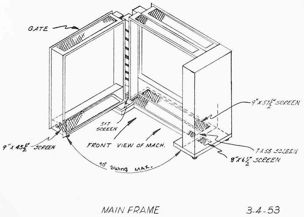
Based on my research, the earliest computer to use the term "main frame" was the IBM 701 computer (1952), which consisted of boxes called "frames." The 701 system consisted of two power frames, a power distribution frame, an electrostatic storage frame, a drum frame, tape frames, and most importantly a main frame. The IBM 701's main frame is shown in the documentation below.2

This diagram shows how the IBM 701 mainframe swings open for access to the circuitry. From "Type 701 EDPM Installation Manual", IBM. From Computer History Museum archives.

This diagram shows how the IBM 701 mainframe swings open for access to the circuitry. From "Type 701 EDPM [Electronic Data Processing Machine] Installation Manual", IBM. From Computer History Museum archives.

The meaning of "mainframe" has evolved, shifting from being a part of a computer to being a type of computer. For decades, "mainframe" referred to the physical box of the computer; unlike modern usage, this "mainframe" could be a minicomputer or even microcomputer. Simultaneously, "mainframe" was a synonym for "central processing unit." In the 1970s, the modern meaning started to develop—a large, powerful computer for transaction processing or business applications—but it took decades for this meaning to replace the earlier ones. In this article, I'll examine the history of these shifting meanings in detail.

Early computers and the origin of "main frame"

Early computers used a variety of mounting and packaging techniques including panels, cabinets, racks, and bays.3 This packaging made it very difficult to install or move a computer, often requiring cranes or the removal of walls.4 To avoid these problems, the designers of the IBM 701 computer came up with an innovative packaging technique. This computer was constructed as individual units that would pass through a standard doorway, would fit on a standard elevator, and could be transported with normal trucking or aircraft facilities.7 These units were built from a metal frame with covers attached, so each unit was called a frame. The frames were named according to their function, such as the power frames and the tape frame. Naturally, the main part of the computer was called the main frame.

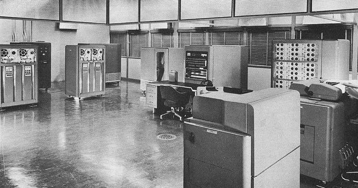
An IBM 701 system at General Motors. On the left: tape drives in front of power frames. Back: drum unit/frame, control panel and electronic analytical control unit (main frame), electrostatic storage unit/frame (with circular storage CRTs). Right: printer, card punch. Photo from BRL Report, thanks to Ed Thelen.

An IBM 701 system at General Motors. On the left: tape drives in front of power frames. Back: drum unit/frame, control panel and electronic analytical control unit (main frame), electrostatic storage unit/frame (with circular storage CRTs). Right: printer, card punch. Photo from BRL Report, thanks to Ed Thelen.

The IBM 701's internal documentation used "main frame" frequently to indicate the main box of the computer, alongside "power frame", "core frame", and so forth. For instance, each component in the schematics was labeled with its location in the computer, "MF" for the main frame.6 Externally, however, IBM documentation described the parts of the 701 computer as units rather than frames.5

The term "main frame" was used by a few other computers in the 1950s.8 For instance, the JOHNNIAC Progress Report (August 8, 1952) mentions that "the main frame for the JOHNNIAC is ready to receive registers" and they could test the arithmetic unit "in the JOHNNIAC main frame in October."10 An article on the RAND Computer in 1953 stated that "The main frame is completed and partially wired" The main body of a computer called ERMA is labeled "main frame" in the 1955 Proceedings of the Eastern Computer Conference.9

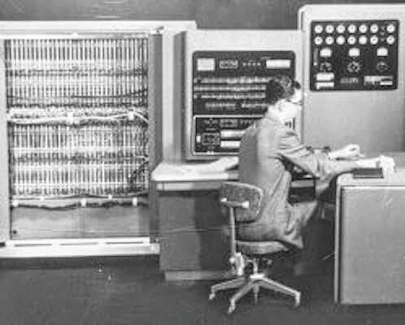
Operator at console of IBM 701. The main frame is on the left with the cover removed. The console is in the center. The power frame (with gauges) is on the right. Photo from NOAA.

Operator at console of IBM 701. The main frame is on the left with the cover removed. The console is in the center. The power frame (with gauges) is on the right. Photo from NOAA.

The progression of the word "main frame" can be seen in reports from the Ballistics Research Lab (BRL) that list almost all the computers in the United States. In the 1955 BRL report, most computers were built from cabinets or racks; the phrase "main frame" was only used with the IBM 650, 701, and 704. By 1961, the BRL report shows "main frame" appearing in descriptions of the IBM 702, 705, 709, and 650 RAMAC, as well as the Univac FILE 0, FILE I, RCA 501, READIX, and Teleregister Telefile. This shows that the use of "main frame" was increasing, but still mostly an IBM term.

The physical box of a minicomputer or microcomputer

In modern usage, mainframes are distinct from minicomputers or microcomputers. But until the 1980s, the word "mainframe" could also mean the main physical part of a minicomputer or microcomputer. For instance, a "minicomputer mainframe" was not a powerful minicomputer, but simply the main part of a minicomputer.13 For example, the PDP-11 is an iconic minicomputer, but DEC discussed its "mainframe."14. Similarly, the desktop-sized HP 2115A and Varian Data 620i computers also had mainframes.15 As late as 1981, the book Mini and Microcomputers mentioned "a minicomputer mainframe."

"Mainframes for Hobbyists" on the front cover of Radio-Electronics, Feb 1978.

"Mainframes for Hobbyists" on the front cover of Radio-Electronics, Feb 1978.

Even microcomputers had a mainframe: the cover of Radio Electronics (1978, above) stated, "Own your own Personal Computer: Mainframes for Hobbyists", using the definition below. An article "Introduction to Personal Computers" in Radio Electronics (Mar 1979) uses a similar meaning: "The first choice you will have to make is the mainframe or actual enclosure that the computer will sit in." The popular hobbyist magazine BYTE also used "mainframe" to describe a microprocessor's box in the 1970s and early 1980s16. BYTE sometimes used the word "mainframe" both to describe a large IBM computer and to describe a home computer box in the same issue, illustrating that the two distinct meanings coexisted.

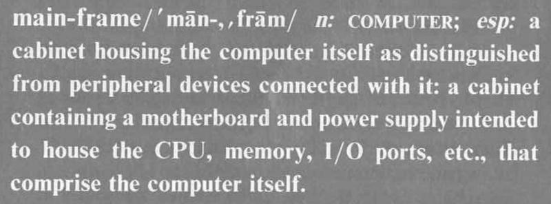
Definition from Radio-Electronics: main-frame n: COMPUTER; esp: a cabinet housing the computer itself as distinguished from peripheral devices connected with it: a cabinet containing a motherboard and power supply intended to house the CPU, memory, I/O ports, etc., that comprise the computer itself.

Definition from Radio-Electronics: main-frame n: COMPUTER; esp: a cabinet housing the computer itself as distinguished from peripheral devices connected with it: a cabinet containing a motherboard and power supply intended to house the CPU, memory, I/O ports, etc., that comprise the computer itself.

Main frame synonymous with CPU

Words often change meaning through metonymy, where a word takes on the meaning of something closely associated with the original meaning. Through this process, "main frame" shifted from the physical frame (as a box) to the functional contents of the frame, specifically the central processing unit.17

The earliest instance that I could find of the "main frame" being equated with the central processing unit was in 1955. Survey of Data Processors stated: "The central processing unit is known by other names; the arithmetic and ligical [sic] unit, the main frame, the computer, etc. but we shall refer to it, usually, as the central processing unit." A similar definition appeared in Radio Electronics (June 1957, p37): "These arithmetic operations are performed in what is called the arithmetic unit of the machine, also sometimes referred to as the 'main frame.'"

The US Department of Agriculture's Glossary of ADP Terminology (1960) uses the definition: "MAIN FRAME - The central processor of the computer system. It contains the main memory, arithmetic unit and special register groups." I'll mention that "special register groups" is nonsense that was repeated for years.18 This definition was reused and extended in the government's Automatic Data Processing Glossary, published in 1962 "for use as an authoritative reference by all officials and employees of the executive branch of the Government" (below). This definition was reused in many other places, notably the Oxford English Dictionary.19

Definition from Bureau of the Budget: frame, main, (1) the central processor of the computer system. It contains the main storage, arithmetic unit and special register groups. Synonymous with (CPU) and (central processing unit). (2) All that portion of a computer exclusive of the input, output, peripheral and in some instances, storage units.

Definition from Bureau of the Budget: frame, main, (1) the central processor of the computer system. It contains the main storage, arithmetic unit and special register groups. Synonymous with (CPU) and (central processing unit). (2) All that portion of a computer exclusive of the input, output, peripheral and in some instances, storage units.

By the early 1980s, defining a mainframe as the CPU had become obsolete. IBM stated that "mainframe" was a deprecated term for "processing unit" in the Vocabulary for Data Processing, Telecommunications, and Office Systems (1981); the American National Dictionary for Information Processing Systems (1982) was similar. Computers and Business Information Processing (1983) bluntly stated: "According to the official definition, 'mainframe' and 'CPU' are synonyms. Nobody uses the word mainframe that way."

Mainframe vs. peripherals

Rather than defining the mainframe as the CPU, some dictionaries defined the mainframe in opposition to the "peripherals", the computer's I/O devices. The two definitions are essentially the same, but have a different focus.20 One example is the IFIP-ICC Vocabulary of Information Processing (1966) which defined "central processor" and "main frame" as "that part of an automatic data processing system which is not considered as peripheral equipment." Computer Dictionary (1982) had the definition "main frame—The fundamental portion of a computer, i.e. the portion that contains the CPU and control elements of a computer system, as contrasted with peripheral or remote devices usually of an input-output or memory nature."

One reason for this definition was that computer usage was billed for mainframe time, while other tasks such as printing results could save money by taking place directly on the peripherals without using the mainframe itself.21 A second reason was that the mainframe vs. peripheral split mirrored the composition of the computer industry, especially in the late 1960s and 1970s. Computer systems were built by a handful of companies, led by IBM. Compatible I/O devices and memory were built by many other companies that could sell them at a lower cost than IBM.22 Publications about the computer industry needed convenient terms to describe these two industry sectors, and they often used "mainframe manufacturers" and "peripheral manufacturers."

Main Frame or Mainframe?

An interesting linguistic shift is from "main frame" as two independent words to a compound word: either hyphenated "main-frame" or the single word "mainframe." This indicates the change from "main frame" being a type of frame to "mainframe" being a new concept. The earliest instance of hyphenated "main-frame" that I found was from 1959 in IBM Information Retrieval Systems Conference. "Mainframe" as a single, non-hyphenated word appears the same year in Datamation, mentioning the mainframe of the NEAC2201 computer. In 1962, the IBM 7090 Installation Instructions refer to a "Mainframe Diag[nostic] and Reliability Program." (Curiously, the document also uses "main frame" as two words in several places.) The 1962 book Information Retrieval Management discusses how much computer time document queries can take: "A run of 100 or more machine questions may require two to five minutes of mainframe time." This shows that by 1962, "main frame" had semantically shifted to a new word, "mainframe."

The rise of the minicomputer and how the "mainframe" become a class of computers

So far, I've shown how "mainframe" started as a physical frame in the computer, and then was generalized to describe the CPU. But how did "mainframe" change from being part of a computer to being a class of computers? This was a gradual process, largely happening in the mid-1970s as the rise of the minicomputer and microcomputer created a need for a word to describe large computers.

Although microcomputers, minicomputers, and mainframes are now viewed as distinct categories, this was not the case at first. For instance, a 1966 computer buyer's guide lumps together computers ranging from desk-sized to 70,000 square feet.23 Around 1968, however, the term "minicomputer" was created to describe small computers. The story is that the head of DEC in England created the term, inspired by the miniskirt and the Mini Minor car.24 While minicomputers had a specific name, larger computers did not.25

Gradually in the 1970s "mainframe" came to be a separate category, distinct from "minicomputer."2627 An early example is Datamation (1970), describing systems of various sizes: "mainframe, minicomputer, data logger, converters, readers and sorters, terminals." The influential business report EDP first split mainframes from minicomputers in 1972.28 The line between minicomputers and mainframes was controversial, with articles such as Distinction Helpful for Minis, Mainframes and Micro, Mini, or Mainframe? Confusion persists (1981) attempting to clarify the issue.29

With the development of the microprocessor, computers became categorized as mainframes, minicomputers or microcomputers. For instance, a 1975 Computerworld article discussed how the minicomputer competes against the microcomputer and mainframes. Adam Osborne's An Introduction to Microcomputers (1977) described computers as divided into mainframes, minicomputers, and microcomputers by price, power, and size. He pointed out the large overlap between categories and avoided specific definitions, stating that "A minicomputer is a minicomputer, and a mainframe is a mainframe, because that is what the manufacturer calls it."32

In the late 1980s, computer industry dictionaries started defining a mainframe as a large computer, often explicitly contrasted with a minicomputer or microcomputer. By 1990, they mentioned the networked aspects of mainframes.33

IBM embraces the mainframe label

Even though IBM is almost synonymous with "mainframe" now, IBM avoided marketing use of the word for many years, preferring terms such as "general-purpose computer."35 IBM's book Planning a Computer System (1962) repeatedly referred to "general-purpose computers" and "large-scale computers", but never used the word "mainframe."34 The announcement of the revolutionary System/360 (1964) didn't use the word "mainframe"; it was called a general-purpose computer system. The announcement of the System/370 (1970) discussed "medium- and large-scale systems." The System/32 introduction (1977) said, "System/32 is a general purpose computer..." The 1982 announcement of the 3804, IBM's most powerful computer at the time, called it a "large scale processor" not a mainframe.

IBM started using "mainframe" as a marketing term in the mid-1980s. For example, the 3270 PC Guide (1986) refers to "IBM mainframe computers." An IBM 9370 Information System brochure (c. 1986) says the system was "designed to provide mainframe power." IBM's brochure for the 3090 processor (1987) called them "advanced general-purpose computers" but also mentioned "mainframe computers." A System 390 brochure (c. 1990) discussed "entry into the mainframe class." The 1990 announcement of the ES/9000 called them "the most powerful mainframe systems the company has ever offered."

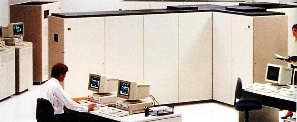
The IBM System/390: "The excellent balance between price and performance makes entry into the mainframe class an attractive proposition." IBM System/390 Brochure

The IBM System/390: "The excellent balance between price and performance makes entry into the mainframe class an attractive proposition." IBM System/390 Brochure

By 2000, IBM had enthusiastically adopted the mainframe label: the z900 announcement used the word "mainframe" six times, calling it the "reinvented mainframe." In 2003, IBM announced "The Mainframe Charter", describing IBM's "mainframe values" and "mainframe strategy." Now, IBM has retroactively applied the name "mainframe" to their large computers going back to 1959 (link), (link).

Mainframes and the general public

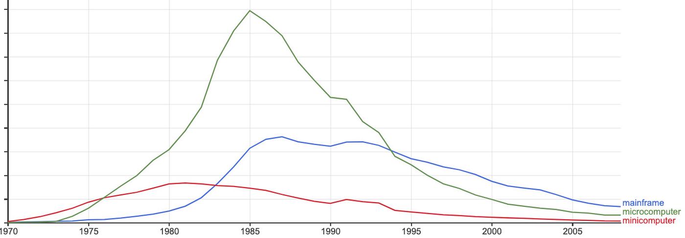
While "mainframe" was a relatively obscure computer term for many years, it became widespread in the 1980s. The Google Ngram graph below shows the popularity of "microcomputer", "minicomputer", and "mainframe" in books.36 The terms became popular during the late 1970s and 1980s. The popularity of "minicomputer" and "microcomputer" roughly mirrored the development of these classes of computers. Unexpectedly, even though mainframes were the earliest computers, the term "mainframe" peaked later than the other types of computers.

N-gram graph from Google Books Ngram Viewer.

N-gram graph from Google Books Ngram Viewer.

Dictionary definitions

I studied many old dictionaries to see when the word "mainframe" showed up and how they defined it. To summarize, "mainframe" started to appear in dictionaries in the late 1970s, first defining the mainframe in opposition to peripherals or as the CPU. In the 1980s, the definition gradually changed to the modern definition, with a mainframe distinguished as being large, fast, and often centralized system. These definitions were roughly a decade behind industry usage, which switched to the modern meaning in the 1970s.

The word didn't appear in older dictionaries, such as the Random House College Dictionary (1968) and Merriam-Webster (1974). The earliest definition I could find was in the supplement to Webster's International Dictionary (1976): "a computer and esp. the computer itself and its cabinet as distinguished from peripheral devices connected with it." Similar definitions appeared in Webster's New Collegiate Dictionary (1976, 1980).

A CPU-based definition appeared in Random House College Dictionary (1980): "the device within a computer which contains the central control and arithmetic units, responsible for the essential control and computational functions. Also called central processing unit." The Random House Dictionary (1978, 1988 printing) was similar. The American Heritage Dictionary (1982, 1985) combined the CPU and peripheral approaches: "mainframe. The central processing unit of a computer exclusive of peripheral and remote devices."
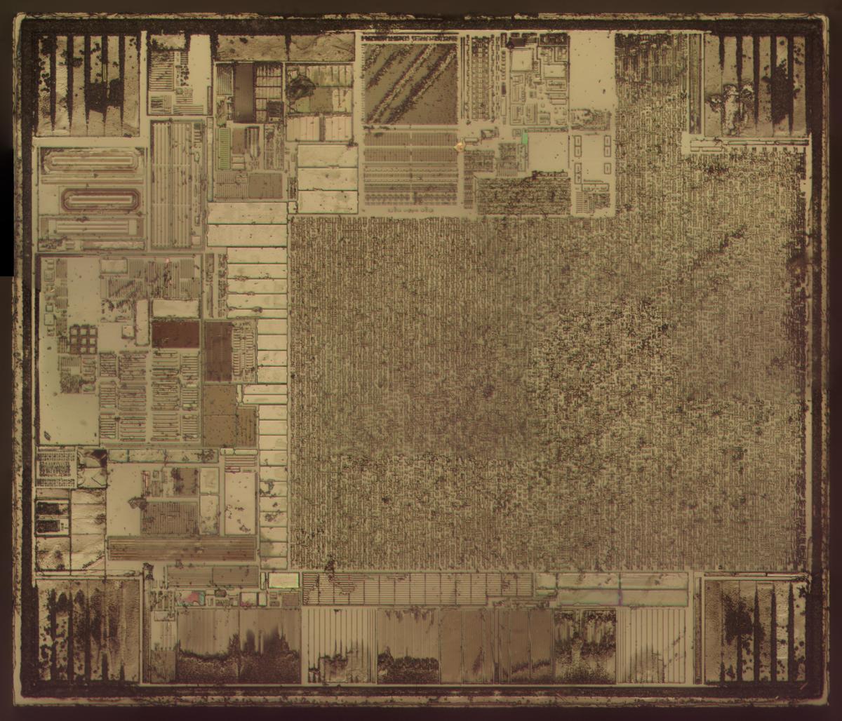
The modern definition as a large computer appeared alongside the old definition in Webster's Ninth New Collegiate Dictionary (1983): "mainframe (1964): a computer with its cabinet and internal circuits; also: a large fast computer that can handle multiple tasks concurrently." Only the modern definition appears in The New Merriram-Webster Dictionary (1989): "large fast computer", while Webster's Unabridged Dictionary of the English Language (1989): "mainframe. a large high-speed computer with greater storage capacity than a minicomputer, often serving as the central unit in a system of smaller computers. [MAIN + FRAME]." Random House Webster's College Dictionary (1991) and Random House College Dictionary (2001) had similar definitions.

The Oxford English Dictionary is the principal historical dictionary, so it is interesting to see its view. The 1989 OED gave historical definitions as well as defining mainframe as "any large or general-purpose computer, exp. one supporting numerous peripherals or subordinate computers." It has seven historical examples from 1964 to 1984; the earliest is the 1964 Honeywell Glossary. It quotes a 1970 Dictionary of Computers as saying that the word "Originally implied the main framework of a central processing unit on which the arithmetic unit and associated logic circuits were mounted, but now used colloquially to refer to the central processor itself." The OED also cited a Hewlett-Packard ad from 1974 that used the word "mainframe", but I consider this a mistake as the usage is completely different.15

Encyclopedias

A look at encyclopedias shows that the word "mainframe" started appearing in discussions of computers in the early 1980s, later than in dictionaries. At the beginning of the 1980s, many encyclopedias focused on large computers, without using the word "mainframe", for instance, The Concise Encyclopedia of the Sciences (1980) and World Book (1980). The word "mainframe" started to appear in supplements such as Britannica Book of the Year (1980) and World Book Year Book (1981), at the same time as they started discussing microcomputers. Soon encyclopedias were using the word "mainframe", for example, Funk & Wagnalls Encyclopedia (1983), Encyclopedia Americana (1983), and World Book (1984). By 1986, even the Doubleday Children's Almanac showed a "mainframe computer."

Newspapers

I examined old newspapers to track the usage of the word "mainframe." The graph below shows the usage of "mainframe" in newspapers. The curve shows a rise in popularity through the 1980s and a steep drop in the late 1990s. The newspaper graph roughly matches the book graph above, although newspapers show a much steeper drop in the late 1990s. Perhaps mainframes aren't in the news anymore, but people still write books about them.

Newspaper usage of "mainframe." Graph from newspapers.com from 1975 to 2010 shows usage started growing in 1978, picked up in 1984, and peaked in 1989 and 1997, with a large drop in 2001 and after (y2k?).

Newspaper usage of "mainframe." Graph from newspapers.com from 1975 to 2010 shows usage started growing in 1978, picked up in 1984, and peaked in 1989 and 1997, with a large drop in 2001 and after (y2k?).

The first newspaper appearances were in classified ads seeking employees, for instance, a 1960 ad in the San Francisco Examiner for people "to monitor and control main-frame operations of electronic computers...and to operate peripheral equipment..." and a (sexist) 1966 ad in the Philadelphia Inquirer for "men with Digital Computer Bkgrnd [sic] (Peripheral or Mainframe)."37

By 1970, "mainframe" started to appear in news articles, for example, "The computer can't work without the mainframe unit." By 1971, the usage increased with phrases such as "mainframe central processor" and "'main-frame' computer manufacturers". 1972 had usages such as "the mainframe or central processing unit is the heart of any computer, and does all the calculations". A 1975 article explained "'Mainframe' is the industry's word for the computer itself, as opposed to associated items such as printers, which are referred to as 'peripherals.'" By 1980, minicomputers and microcomputers were appearing: "All hardware categories-mainframes, minicomputers, microcomputers, and terminals" and "The mainframe and the minis are interconnected."

By 1985, the mainframe was a type of computer, not just the CPU: "These days it's tough to even define 'mainframe'. One definition is that it has for its electronic brain a central processor unit (CPU) that can handle at least 32 bits of information at once. ... A better distinction is that mainframes have numerous processors so they can work on several jobs at once." Articles also discussed "the micro's challenge to the mainframe" and asked, "buy a mainframe, rather than a mini?"

By 1990, descriptions of mainframes became florid: "huge machines laboring away in glass-walled rooms", "the big burner which carries the whole computing load for an organization", "behemoth data crunchers", "the room-size machines that dominated computing until the 1980s", "the giant workhorses that form the nucleus of many data-processing centers", "But it is not raw central-processing-power that makes a mainframe a mainframe. Mainframe computers command their much higher prices because they have much more sophisticated input/output systems."

Conclusion

After extensive searches through archival documents, I found usages of the term "main frame" dating back to 1952, much earlier than previously reported. In particular, the introduction of frames to package the IBM 701 computer led to the use of the word "main frame" for that computer and later ones. The term went through various shades of meaning and remained fairly obscure for many years. In the mid-1970s, the term started describing a large computer, essentially its modern meaning. In the 1980s, the term escaped the computer industry and appeared in dictionaries, encyclopedias, and newspapers. After peaking in the 1990s, the term declined in usage (tracking the decline in mainframe computers), but the term and the mainframe computer both survive.

Two factors drove the popularity of the word "mainframe" in the 1980s with its current meaning of a large computer. First, the terms "microcomputer" and "minicomputer" led to linguistic pressure for a parallel term for large computers. For instance, the business press needed a word to describe IBM and other large computer manufacturers. While "server" is the modern term, "mainframe" easily filled the role back then and was nicely alliterative with "microcomputer" and "minicomputer."38

Second, up until the 1980s, the prototype meaning for "computer" was a large mainframe, typically IBM.39 But as millions of home computers were sold in the early 1980s, the prototypical "computer" shifted to smaller machines. This left a need for a term for large computers, and "mainframe" filled that need. In other words, if you were talking about a large computer in the 1970s, you could say "computer" and people would assume you meant a mainframe. But if you said "computer" in the 1980s, you needed to clarify if it was a large computer.

The word "mainframe" is almost 75 years old and both the computer and the word have gone through extensive changes in this time. The "death of the mainframe" has been proclaimed for well over 30 years but mainframes are still hanging on. Who knows what meaning "mainframe" will have in another 75 years?

Follow me on Bluesky (@righto.com) or RSS. (I'm no longer on Twitter.) Thanks to the Computer History Museum and archivist Sara Lott for access to many documents.

Notes and References

  1. The Computer History Museum states: "Why are they called “Mainframes”? Nobody knows for sure. There was no mainframe “inventor” who coined the term. Probably “main frame” originally referred to the frames (designed for telephone switches) holding processor circuits and main memory, separate from racks or cabinets holding other components. Over time, main frame became mainframe and came to mean 'big computer.'" (Based on my research, I don't think telephone switches have any connection to computer mainframes.)

    Several sources explain that the mainframe is named after the frame used to construct the computer. The Jargon File has a long discussion, stating that the term "originally referring to the cabinet containing the central processor unit or ‘main frame’." Ken Uston's Illustrated Guide to the IBM PC (1984) has the definition "MAIN FRAME A large, high-capacity computer, so named because the CPU of this kind of computer used to be mounted on a frame." IBM states that mainframe "Originally referred to the central processing unit of a large computer, which occupied the largest or central frame (rack)." The Microsoft Computer Dictionary (2002) states that the name mainframe "is derived from 'main frame', the cabinet originally used to house the processing unit of such computers." Some discussions of the origin of the word "mainframe" are here, here, here, here, and here.

    The phrase "main frame" in non-computer contexts has a very old but irrelevant history, describing many things that have a frame. For example, it appears in thousands of patents from the 1800s, including drills, saws, a meat cutter, a cider mill, printing presses, and corn planters. This shows that it was natural to use the phrase "main frame" when describing something constructed from frames. Telephony uses a Main distribution frame or "main frame" for wiring, going back to 1902. Some people claim that the computer use of "mainframe" is related to the telephony use, but I don't think they are related. In particular, a telephone main distribution frame looks nothing like a computer mainframe. Moreover, the computer use and the telephony use developed separately; if the computer use started in, say, Bell Labs, a connection would be more plausible.

    IBM patents with "main frame" include a scale (1922), a card sorter (1927), a card duplicator (1929), and a card-based accounting machine (1930). IBM's incidental uses of "main frame" are probably unrelated to modern usage, but they are a reminder that punch card data processing started decades before the modern computer. 

  2. It is unclear why the IBM 701 installation manual is dated August 27, 1952 but the drawing is dated 1953. I assume the drawing was updated after the manual was originally produced. 

  3. This footnote will survey the construction techniques of some early computers; the key point is that building a computer on frames was not an obvious technique. ENIAC (1945), the famous early vacuum tube computer, was constructed from 40 panels forming three walls filling a room (ref, ref). EDVAC (1949) was built from large cabinets or panels (ref) while ORDVAC and CLADIC (1949) were built on racks (ref). One of the first commercial computers, UNIVAC 1 (1951), had a "Central Computer" organized as bays, divided into three sections, with tube "chassis" plugged in (ref ). The Raytheon computer (1951) and Moore School Automatic Computer (1952) (ref) were built from racks. The MONROBOT VI (1955) was described as constructed from the "conventional rack-panel-cabinet form" (ref). 

  4. The size and construction of early computers often made it difficult to install or move them. The early computer ENIAC required 9 months to move from Philadelphia to the Aberdeen Proving Ground. For this move, the wall of the Moore School in Philadelphia had to be partially demolished so ENIAC's main panels could be removed. In 1959, moving the SWAC computer required disassembly of the computer and removing one wall of the building (ref). When moving the early computer JOHNNIAC to a different site, the builders discovered the computer was too big for the elevator. They had to raise the computer up the elevator shaft without the elevator (ref). This illustrates the benefits of building a computer from moveable frames. 

  5. The IBM 701's main frame was called the Electronic Analytical Control Unit in external documentation. 

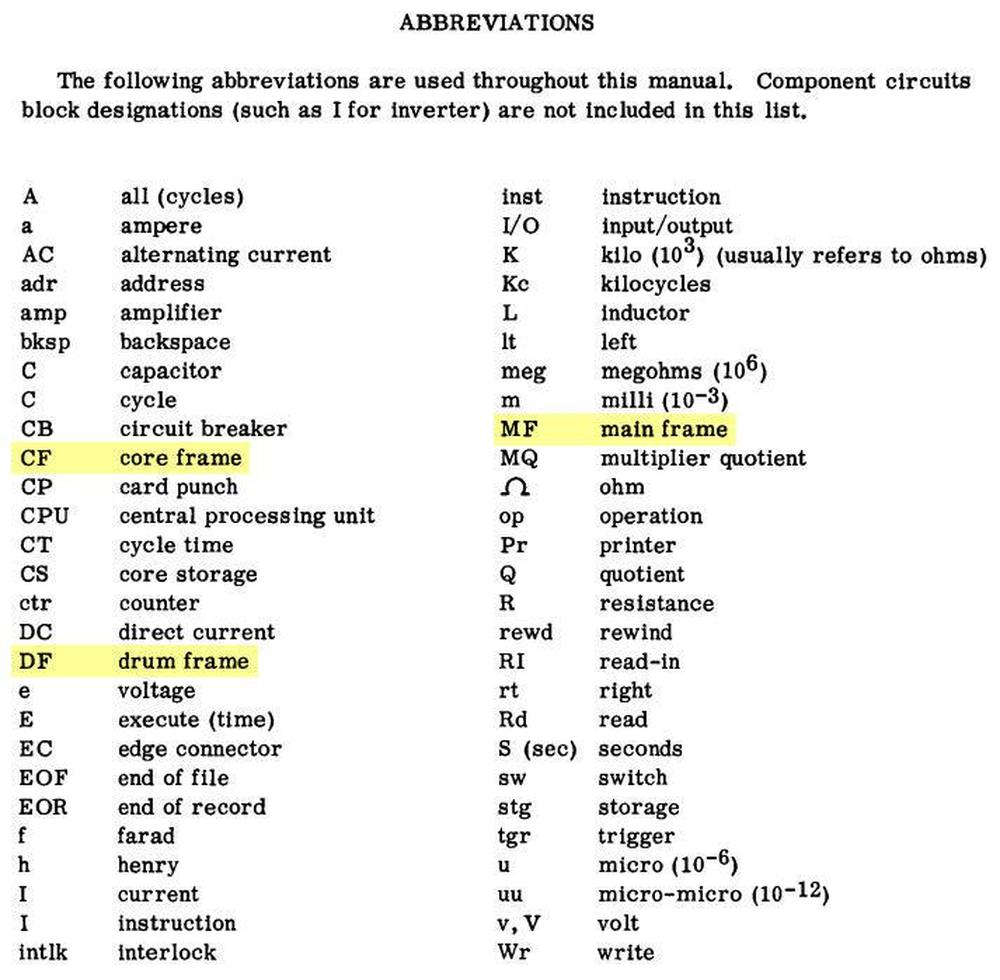
  6. The 701 installation manual (1952) has a frame arrangement diagram showing the dimensions of the various frames, along with a drawing of the main frame, and power usage of the various frames. Service documentation (1953) refers to "main frame adjustments" (page 74). The 700 Series Data Processing Systems Component Circuits document (1955-1959) lists various types of frames in its abbreviation list (below)

    Abbreviations used in IBM drawings include MF for main frame. Also note CF for core frame, and DF for drum frame, From 700 Series Data Processing Systems Component Circuits (1955-1959).

    Abbreviations used in IBM drawings include MF for main frame. Also note CF for core frame, and DF for drum frame, From 700 Series Data Processing Systems Component Circuits (1955-1959).

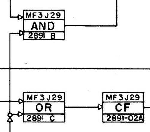
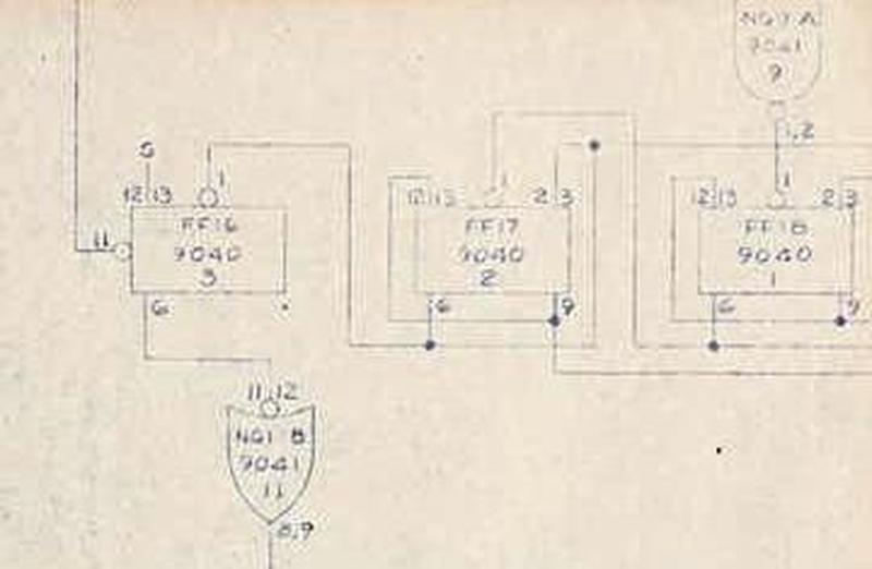
    When repairing an IBM 701, it was important to know which frame held which components, so "main frame" appeared throughout the engineering documents. For instance, in the schematics, each module was labeled with its location; "MF" stands for "main frame."

    Detail of a 701 schematic diagram. "MF" stands for "main frame." This diagram shows part of a pluggable tube module (type 2891) in mainframe panel 3 (MF3) section J, column 29.
The blocks shown are an AND gate, OR gate, and Cathode Follower (buffer).
From System Drawings 1.04.1.

    Detail of a 701 schematic diagram. "MF" stands for "main frame." This diagram shows part of a pluggable tube module (type 2891) in mainframe panel 3 (MF3) section J, column 29. The blocks shown are an AND gate, OR gate, and Cathode Follower (buffer). From System Drawings 1.04.1.

    The "main frame" terminology was used in discussions with customers. For example, notes from a meeting with IBM (April 8, 1952) mention "E. S. [Electrostatic] Memory 15 feet from main frame" and list "main frame" as one of the seven items obtained for the $15,000/month rental cost.  

  7. For more information on how the IBM 701 was designed to fit on elevators and through doorways, see Building IBM: Shaping an Industry and Technology page 170, and The Interface: IBM and the Transformation of Corporate Design page 69. This is also mentioned in "Engineering Description of the IBM Type 701 Computer", Proceedings of the IRE Oct 1953, page 1285. 

  8. Many early systems used "central computer" to describe the main part of the computer, perhaps more commonly than "main frame." An early example is the "central computer" of the Elecom 125 (1954). The Digital Computer Newsletter (Apr 1955) used "central computer" several times to describe the processor of SEAC. The 1961 BRL report shows "central computer" being used by Univac II, Univac 1107, Univac File 0, DYSEAC and RCA Series 300. The MIT TX-2 Technical Manual (1961) uses "central computer" very frequently. The NAREC glossary (1962) defined "central computer. That part of a computer housed in the main frame." 

  9. This footnote lists some other early computers that used the term "main frame." The October 1956 Digital Computer Newsletter mentions the "main frame" of the IBM NORC. Digital Computer Newsletter (Jan 1959) discusses using a RAMAC disk drive to reduce "main frame processing time." This document also mentions the IBM 709 "main frame." The IBM 704 documentation (1958) says "Each DC voltage is distributed to the main frame..." (IBM 736 reference manual) and "Check the air filters in each main frame unit and replace when dirty." (704 Central Processing Unit).

    The July 1962 Digital Computer Newsletter discusses the LEO III computer: "It has been built on the modular principle with the main frame, individual blocks of storage, and input and output channels all physically separate." The article also mentions that the new computer is more compact with "a reduction of two cabinets for housing the main frame."

    The IBM 7040 (1964) and IBM 7090 (1962) were constructed from multiple frames, including the processing unit called the "main frame."11 Machines in IBM's System/360 line (1964) were built from frames; some models had a main frame, power frame, wall frame, and so forth, while other models simply numbered the frames sequentially.12 

  10. The 1952 JOHNNIAC progress report is quoted in The History of the JOHNNIAC. This memorandum was dated August 8, 1952, so it is the earliest citation that I found. The June 1953 memorandum also used the term, stating, "The main frame is complete." 

  11. A detailed description of IBM's frame-based computer packaging is in Standard Module System Component Circuits pages 6-9. This describes the SMS-based packaging used in the IBM 709x computers, the IBM 1401, and related systems as of 1960. 

  12. IBM System/360 computers could have many frames, so they were usually given sequential numbers. The Model 85, for instance, had 12 frames for the processor and four megabytes of memory in 18 frames (at over 1000 pounds each). Some of the frames had descriptive names, though. The Model 40 had a main frame (CPU main frame, CPU frame), a main storage logic frame, a power supply frame, and a wall frame. The Model 50 had a CPU frame, power frame, and main storage frame. The Model 75 had a main frame (consisting of multiple physical frames), storage frames, channel frames, central processing frames, and a maintenance console frame. The compact Model 30 consisted of a single frame, so the documentation refers to the "frame", not the "main frame." For more information on frames in the System/360, see 360 Physical Planning. The Architecture of the IBM System/360 paper refers to the "main-frame hardware." 

  13. A few more examples that discuss the minicomputer's mainframe, its physical box: A 1970 article discusses the mainframe of a minicomputer (as opposed to the peripherals) and contrasts minicomputers with large scale computers. A 1971 article on minicomputers discusses "minicomputer mainframes." Computerworld (Jan 28, 1970, p59) discusses minicomputer purchases: "The actual mainframe is not the major cost of the system to the user." Modern Data (1973) mentions minicomputer mainframes several times. 

  14. DEC documents refer to the PDP-11 minicomputer as a mainframe. The PDP-11 Conventions manual (1970) defined: "Processor: A unit of a computing system that includes the circuits controlling the interpretation and execution of instructions. The processor does not include the Unibus, core memory, interface, or peripheral devices. The term 'main frame' is sometimes used but this term refers to all components (processor, memory, power supply) in the basic mounting box." In 1976, DEC published the PDP-11 Mainframe Troubleshooting Guide. The PDP-11 mainframe is also mentioned in Computerworld (1977). 

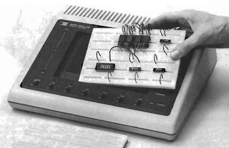
  15. Test equipment manufacturers started using the term "main frame" (and later "mainframe") around 1962, to describe an oscilloscope or other test equipment that would accept plug-in modules. I suspect this is related to the use of "mainframe" to describe a computer's box, but it could be independent. Hewlett-Packard even used the term to describe a solderless breadboard, the 5035 Logic Lab. The Oxford English Dictionary (1989) used HP's 1974 ad for the Logic Lab as its earliest citation of mainframe as a single word. It appears that the OED confused this use of "mainframe" with the computer use.

    Is this a mainframe? The HP 5035A Logic Lab was a power supply and support circuitry for a solderless breadboard. HP's ads referred to this as a "laboratory station mainframe."

    Is this a mainframe? The HP 5035A Logic Lab was a power supply and support circuitry for a solderless breadboard. HP's ads referred to this as a "laboratory station mainframe."


  16. In the 1980s, the use of "mainframe" to describe the box holding a microcomputer started to conflict with "mainframe" as a large computer. For example, Radio Electronics (October 1982), started using the short-lived term "micro-mainframe" instead of "mainframe" for a microcomputer's enclosure. By 1985, Byte magazine had largely switched to the modern usage of "mainframe." But even as late as 1987, a review of the Apple IIGC described one of the system's components as the '"mainframe" (i.e. the actual system box)'. 

  17. Definitions of "central processing unit" disagreed as to whether storage was part of the CPU, part of the main frame, or something separate. This was largely a consequence of the physical construction of early computers. Smaller computers had memory in the same frame as the processor, while larger computers often had separate storage frames for memory. Other computers had some memory with the processor and some external. Thus, the "main frame" might or might not contain memory, and this ambiguity carried over to definitions of CPU. (In modern usage, the CPU consists of the arithmetic/logic unit (ALU) and control circuitry, but excludes memory.) 

  18. Many definitions of mainframe or CPU mention "special register groups", an obscure feature specific to the Honeywell 800 computer (1959). (Processors have registers, special registers are common, and some processors have register groups, but only the Honeywell 800 had "special register groups.") However, computer dictionaries kept using this phrase for decades, even though it doesn't make sense for other computers. I wrote a blog post about special register groups here

  19. This footnote provides more examples of "mainframe" being defined as the CPU. The Data Processing Equipment Encyclopedia (1961) had a similar definition: "Main Frame: The main part of the computer, i.e. the arithmetic or logic unit; the central processing unit." The 1967 IBM 360 operator's guide defined: "The main frame - the central processing unit and main storage." The Department of the Navy's ADP Glossary (1970): "Central processing unit: A unit of a computer that includes the circuits controlling the interpretation and execution of instructions. Synonymous with main frame." This was a popular definition, originally from the ISO, used by IBM (1979) among others. Funk & Wagnalls Dictionary of Data Processing Terms (1970) defined: "main frame: The basic or essential portion of an assembly of hardware, in particular, the central processing unit of a computer." The American National Standard Vocabulary for Information Processing (1970) defined: "central processing unit: A unit of a computer that includes the circuits controlling the interpretation and execution of instructions. Synonymous with main frame." 

  20. Both the mainframe vs. peripheral definition and the mainframe as CPU definition made it unclear exactly what components of the computer were included in the mainframe. It's clear that the arithmetic-logic unit and the processor control circuitry were included, while I/O devices were excluded, but some components such as memory were in a gray area. It's also unclear if the power supply and I/O interfaces (channels) are part of the mainframe. These distinctions were ignored in almost all of the uses of "mainframe" that I saw.

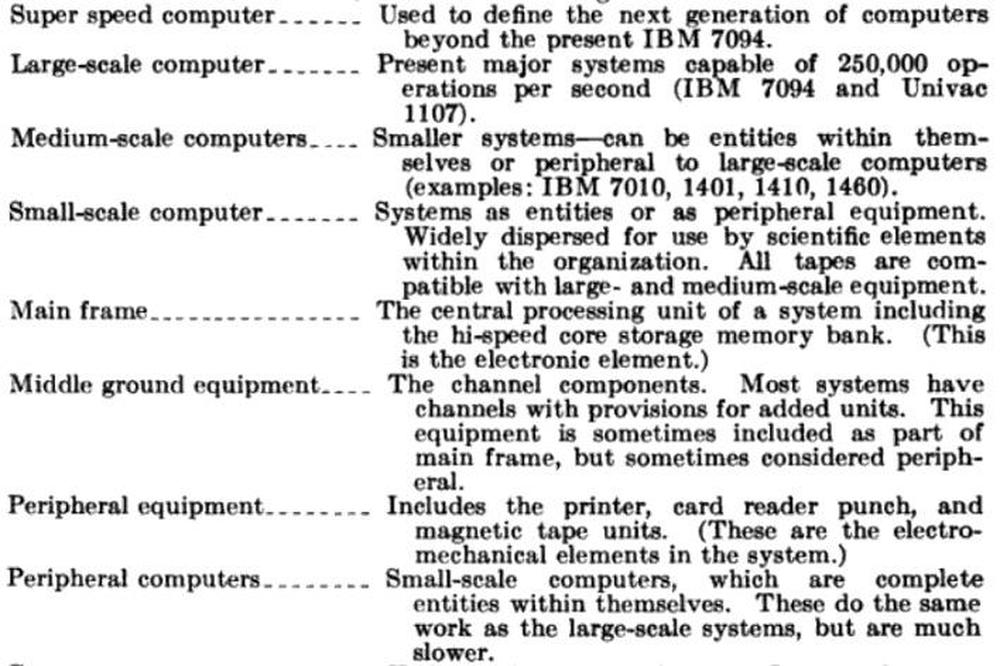
    An unusual definition in a Goddard Space Center document (1965, below) partitioned equipment into the "main frame" (the electronic equipment), "peripheral equipment" (electromechanical components such as the printer and tape), and "middle ground equipment" (the I/O interfaces). The "middle ground" terminology here appears to be unique. Also note that computers are partitioned into "super speed", "large-scale", "medium-scale", and "small-scale."

    Definitions from Automatic Data Processing Equipment, Goddard Space Center, 1965. "Main frame" was defined as "The central processing unit of a system including the hi-speed core storage memory bank. (This is the electronic element.)

    Definitions from Automatic Data Processing Equipment, Goddard Space Center, 1965. "Main frame" was defined as "The central processing unit of a system including the hi-speed core storage memory bank. (This is the electronic element.)


  21. This footnote gives some examples of using peripherals to save the cost of mainframe time. IBM 650 documentation (1956) describes how "Data written on tape by the 650 can be processed by the main frame of the 700 series systems." Univac II Marketing Material (1957) discusses various ways of reducing "main frame time" by, for instance, printing from tape off-line. The USAF Guide for auditing automatic data processing systems (1961) discusses how these "off line" operations make the most efficient use of "the more expensive main frame time." 

  22. Peripheral manufacturers were companies that built tape drives, printers, and other devices that could be connected to a mainframe built by IBM or another company. The basis for the peripheral industry was antitrust action against IBM that led to the 1956 Consent Decree. Among other things, the consent decree forced IBM to provide reasonable patent licensing, which allowed other firms to build "plug-compatible" peripherals. The introduction of the System/360 in 1964 produced a large market for peripherals and IBM's large profit margins left plenty of room for other companies. 

  23. Computers and Automation, March 1965, categorized computers into five classes, from "Teeny systems" (such as the IBM 360/20) renting for $2000/month, through Small, Medium, and Large systems, up to "Family or Economy Size Systems" (such as the IBM 360/92) renting for $75,000 per month. 

  24. The term "minicomputer" was supposedly invented by John Leng, head of DEC's England operations. In the 1960s, he sent back a sales report: "Here is the latest minicomputer activity in the land of miniskirts as I drive around in my Mini Minor", which led to the term becoming popular at DEC. This story is described in The Ultimate Entrepreneur: The Story of Ken Olsen and Digital Equipment Corporation (1988). I'd trust the story more if I could find a reference that wasn't 20 years after the fact. 

  25. For instance, Computers and Automation (1971) discussed the role of the minicomputer as compared to "larger computers." A 1975 minicomputer report compared minicomputers to their "general-purpose cousins." 

  26. This footnote provides more on the split between minicomputers and mainframes. In 1971, Modern Data Products, Systems, Services contained .".. will offer mainframe, minicomputer, and peripheral manufacturers a design, manufacturing, and production facility...." Standard & Poor's Industry Surveys (1972) mentions "mainframes, minicomputers, and IBM-compatible peripherals." Computerworld (1975) refers to "mainframe and minicomputer systems manufacturers."

    The 1974 textbook "Information Systems: Technology, Economics, Applications" couldn't decide if mainframes were a part of the computer or a type of computer separate from minicomputers, saying: "Computer mainframes include the CPU and main memory, and in some usages of the term, the controllers, channels, and secondary storage and I/O devices such as tape drives, disks, terminals, card readers, printers, and so forth. However, the equipment for storage and I/O are usually called peripheral devices. Computer mainframes are usually thought of as medium to large scale, rather than mini-computers."

    Studying U.S. Industrial Outlook reports provides another perspective over time. U.S. Industrial Outlook 1969 divides computers into small, medium-size, and large-scale. Mainframe manufacturers are in opposition to peripheral manufacturers. The same mainframe vs. peripherals opposition appears in U.S. Industrial Outlook 1970 and U.S. Industrial Outlook 1971. The 1971 report also discusses minicomputer manufacturers entering the "maxicomputer market."30 1973 mentions "large computers, minicomputers, and peripherals." U.S. Industrial Outlook 1976 states, "The distinction between mainframe computers, minis, micros, and also accounting machines and calculators should merge into a spectrum." By 1977, the market was separated into "general purpose mainframe computers", "minicomputers and small business computers" and "microprocessors."

    Family Computing Magazine (1984) had a "Dictionary of Computer Terms Made Simple." It explained that "A Digital computer is either a "mainframe", a "mini", or a "micro." Forty years ago, large mainframes were the only size that a computer could be. They are still the largest size, and can handle more than 100,000,000 instructions per second. PER SECOND! [...] Mainframes are also called general-purpose computers." 

  27. In 1974, Congress held antitrust hearings into IBM. The thousand-page report provides a detailed snapshot of the meanings of "mainframe" at the time. For instance, a market analysis report from IDC illustrates the difficulty of defining mainframes and minicomputers in this era (p4952). The "Mainframe Manufacturers" section splits the market into "general-purpose computers" and "dedicated application computers" including "all the so-called minicomputers." Although this section discusses minicomputers, the emphasis is on the manufacturers of traditional mainframes. A second "Plug-Compatible Manufacturers" section discusses companies that manufactured only peripherals. But there's also a separate "Minicomputers" section that focuses on minicomputers (along with microcomputers "which are simply microprocessor-based minicomputers"). My interpretation of this report is the terminology is in the process of moving from "mainframe vs. peripheral" to "mainframe vs. minicomputer." The statement from Research Shareholders Management (p5416) on the other hand discusses IBM and the five other mainframe companies; they classify minicomputer manufacturers separately. (p5425) p5426 mentions "mainframes, small business computers, industrial minicomputers, terminals, communications equipment, and minicomputers." Economist Ralph Miller mentions the central processing unit "(the so-called 'mainframe')" (p5621) and then contrasts independent peripheral manufacturers with mainframe manufacturers (p5622). The Computer Industry Alliance refers to mainframes and peripherals in multiple places, and "shifting the location of a controller from peripheral to mainframe", as well as "the central processing unit (mainframe)" p5099. On page 5290, "IBM on trial: Monopoly tends to corrupt", from Harper's (May 1974), mentions peripherals compatible with "IBM mainframe units—or, as they are called, central processing computers." 

  28. The influential business newsletter EDP provides an interesting view on the struggle to separate the minicomputer market from larger computers. Through 1968, they included minicomputers in the "general-purpose computer" category. But in 1969, they split "general-purpose computers" into "Group A, General Purpose Digital Computers" and "Group B, Dedicated Application Digital Computers." These categories roughly corresponded to larger computers and minicomputers, on the (dubious) assumption that minicomputers were used for a "dedicated application." The important thing to note is that in 1969 they did not use the term "mainframe" for the first category, even though with the modern definition it's the obvious term to use. At the time, EDP used "mainframe manufacturer" or "mainframer"31 to refer to companies that manufactured computers (including minicomputers), as opposed to manufacturers of peripherals. In 1972, EDP first mentioned mainframes and minicomputers as distinct types. In 1973, "microcomputer" was added to the categories. As the 1970s progressed, the separation between minicomputers and mainframes became common. However, the transition was not completely smooth; 1973 included a reference to "mainframe shipments (including minicomputers)."

    To specific, the EDP Industry Report (Nov. 28, 1969) gave the following definitions of the two groups of computers:

    Group A—General Purpose Digital Computers: These comprise the bulk of the computers that have been listed in the Census previously. They are character or byte oriented except in the case of the large-scale scientific machines, which have 36, 48, or 60-bit words. The predominant portion (60% to 80%) of these computers is rented, usually for $2,000 a month or more. Higher level languages such as Fortran, Cobol, or PL/1 are the primary means by which users program these computers.

    Group B—Dedicated Application Digital Computers: This group of computers includes the "mini's" (purchase price below $25,000), the "midi's" ($25,000 to $50,000), and certain larger systems usually designed or used for one dedicated application such as process control, data acquisition, etc. The characteristics of this group are that the computers are usually word oriented (8, 12, 16, or 24-bits per word), the predominant number (70% to 100%) are purchased, and assembly language (at times Fortran) is the predominant means of programming. This type of computer is often sold to an original equipment manufacturer (OEM) for further system integration and resale to the final user.

    These definitions strike me as rather arbitrary. 

  29. In 1981 Computerworld had articles trying to clarify the distinctions between microcomputers, minicomputers, superminicomputers, and mainframes, as the systems started to overlay. One article, Distinction Helpful for Minis, Mainframes said that minicomputers were generally interactive, while mainframes made good batch machines and network hosts. Microcomputers had up to 512 KB of memory, minis were 16-bit machines with 512 KB to 4 MB of memory, costing up to $100,000. Superminis were 16- to 32-bit machines with 4 MB to 8 MB of memory, costing up to $200,000 but with less memory bandwidth than mainframes. Finally, mainframes were 32-bit machines with more than 8 MB of memory, costing over $200,000. Another article Micro, Mini, or Mainframe? Confusion persists described a microcomputer as using an 8-bit architecture and having fewer peripherals, while a minicomputer has a 16-bit architecture and 48 KB to 1 MB of memory. 

  30. The miniskirt in the mid-1960s was shortly followed by the midiskirt and maxiskirt. These terms led to the parallel construction of the terms minicomputer, midicomputer, and maxicomputer.

    The New York Times had a long article Maxi Computers Face Mini Conflict (April 5, 1970) explicitly making the parallel: "Mini vs. Maxi, the reigning issue in the glamorous world of fashion, is strangely enough also a major point of contention in the definitely unsexy realm of computers."

    Although midicomputer and maxicomputer terminology didn't catch on the way minicomputer did, they still had significant use (example, midicomputer examples, maxicomputer examples).

    The miniskirt/minicomputer parallel was done with varying degrees of sexism. One example is Electronic Design News (1969): "A minicomputer. Like the miniskirt, the small general-purpose computer presents the same basic commodity in a more appealing way." 

  31. Linguistically, one indication that a new word has become integrated in the language is when it can be extended to form additional new words. One example is the formation of "mainframers", referring to companies that build mainframes. This word was moderately popular in the 1970s to 1990s. It was even used by the Department of Justice in their 1975 action against IBM where they described the companies in the systems market as the "mainframe companies" or "mainframers." The word is still used today, but usually refers to people with mainframe skills. Other linguistic extensions of "mainframe" include mainframing, unmainframe, mainframed, nonmainframe, and postmainframe

  32. More examples of the split between microcomputers and mainframes: Softwide Magazine (1978) describes "BASIC versions for micro, mini and mainframe computers." MSC, a disk system manufacturer, had drives "used with many microcomputer, minicomputer, and mainframe processor types" (1980). 

  33. Some examples of computer dictionaries referring to mainframes as a size category: Illustrated Dictionary of Microcomputer Terminology (1978) defines "mainframe" as "(1) The heart of a computer system, which includes the CPU and ALU. (2) A large computer, as opposed to a mini or micro." A Dictionary of Minicomputing and Microcomputing (1982) includes the definition of "mainframe" as "A high-speed computer that is larger, faster, and more expensive than the high-end minicomputers. The boundary between a small mainframe and a large mini is fuzzy indeed." The National Bureau of Standards Future Information Technology (1984) defined: "Mainframe is a term used to designate a medium and large scale CPU." The New American Computer Dictionary (1985) defined "mainframe" as "(1) Specifically, the rack(s) holding the central processing unit and the memory of a large computer. (2) More generally, any large computer. 'We have two mainframes and several minis.'" The 1990 ANSI Dictionary for Information Systems (ANSI X3.172-1990) defined: mainframe. A large computer, usually one to which other computers are connected in order to share its resources and computing power. Microsoft Press Computer Dictionary (1991) defined "mainframe computer" as "A high-level computer designed for the most intensive computational tasks. Mainframe computers are often shared by multiple users connected to the computer via terminals." ISO 2382 (1993) defines a mainframe as "a computer, usually in a computer center, with extensive capabilities and resources to which other computers may be connected so that they can share facilities."

    The Microsoft Computer Dictionary (2002) had an amusingly critical definition of mainframe: "A type of large computer system (in the past often water-cooled), the primary data processing resource for many large businesses and organizations. Some mainframe operating systems and solutions are over 40 years old and have the capacity to store year values only as two digits." 

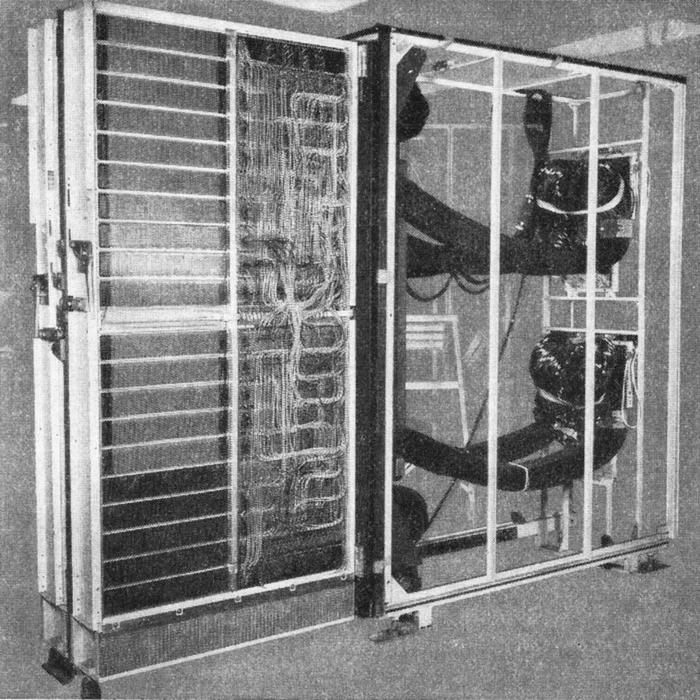
  34. IBM's 1962 book Planning a Computer System (1962) describes how the Stretch computer's circuitry was assembled into frames, with the CPU consisting of 18 frames. The picture below shows how a "frame" was, in fact, constructed from a metal frame.

    In the Stretch computer, the circuitry (left) could be rolled out of the frame (right)

    In the Stretch computer, the circuitry (left) could be rolled out of the frame (right)


  35. The term "general-purpose computer" is probably worthy of investigation since it was used in a variety of ways. It is one of those phrases that seems obvious until you think about it more closely. On the one hand, a computer such as the Apollo Guidance Computer can be considered general purpose because it runs a variety of programs, even though the computer was designed for one specific mission. On the other hand, minicomputers were often contrasted with "general-purpose computers" because customers would buy a minicomputer for a specific application, unlike a mainframe which would be used for a variety of applications. 

  36. The n-gram graph is from the Google Books Ngram Viewer. The curves on the graph should be taken with a grain of salt. First, the usage of words in published books is likely to lag behind "real world" usage. Second, the number of usages in the data set is small, especially at the beginning. Nonetheless, the n-gram graph generally agrees with what I've seen looking at documents directly. 

  37. More examples of "mainframe" in want ads: A 1966 ad from Western Union in The Arizona Republic looking for experience "in a systems engineering capacity dealing with both mainframe and peripherals." A 1968 ad in The Minneapolis Star for an engineer with knowledge of "mainframe and peripheral hardware." A 1968 ad from SDS in The Los Angeles Times for an engineer to design "circuits for computer mainframes and peripheral equipment." A 1968 ad in Fort Lauderdale News for "Computer mainframe and peripheral logic design." A 1972 ad in The Los Angeles Times saying "Mainframe or peripheral [experience] highly desired." In most of these ads, the mainframe was in contrast to the peripherals. 

  38. A related factor is the development of remote connections from a microcomputer to a mainframe in the 1980s. This led to the need for a word to describe the remote computer, rather than saying "I connected my home computer to the other computer." See the many books and articles on connecting "micro to mainframe." 

  39. To see how the prototypical meaning of "computer" changed in the 1980s, I examined the "Computer" article in encyclopedias from that time. The 1980 Concise Encyclopedia of the Sciences discusses a large system with punched-card input. In 1980, the World Book article focused on mainframe systems, starting with a photo of an IBM System/360 Model 40 mainframe. But in the 1981 supplement and the 1984 encyclopedia, the World Book article opened with a handheld computer game, a desktop computer, and a "large-scale computer." The article described microcomputers, minicomputers, and mainframes. Funk & Wagnalls Encyclopedia (1983) was in the middle of the transition; the article focused on large computers and had photos of IBM machines, but mentioned that future growth is expected in microcomputers. By 1994, the World Book article's main focus was the personal computer, although the mainframe still had a few paragraphs and a photo. This is evidence that the prototypical meaning of "computer" underwent a dramatic shift in the early 1980s from a mainframe to a balance between small and large computers, and then to the personal computer. 

Interesting BiCMOS circuits in the Pentium, reverse-engineered

Intel released the powerful Pentium processor in 1993, establishing a long-running brand of processors. Earlier, I wrote about the ROM in the Pentium's floating point unit that holds constants such as π. In this post, I'll look at some interesting circuits associated with this ROM. In particular, the circuitry is implemented in BiCMOS, a process that combines bipolar transistors with standard CMOS logic.

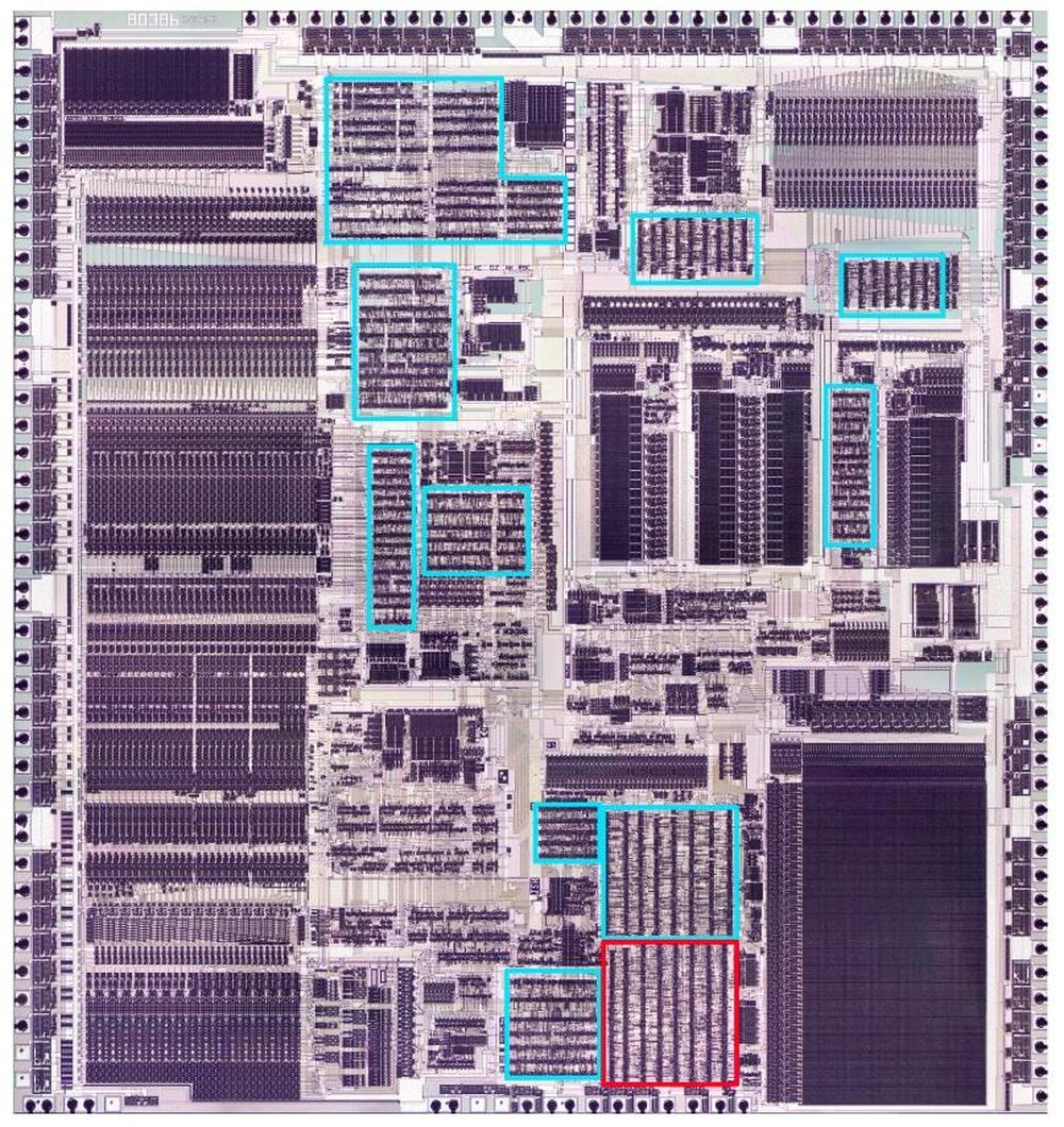
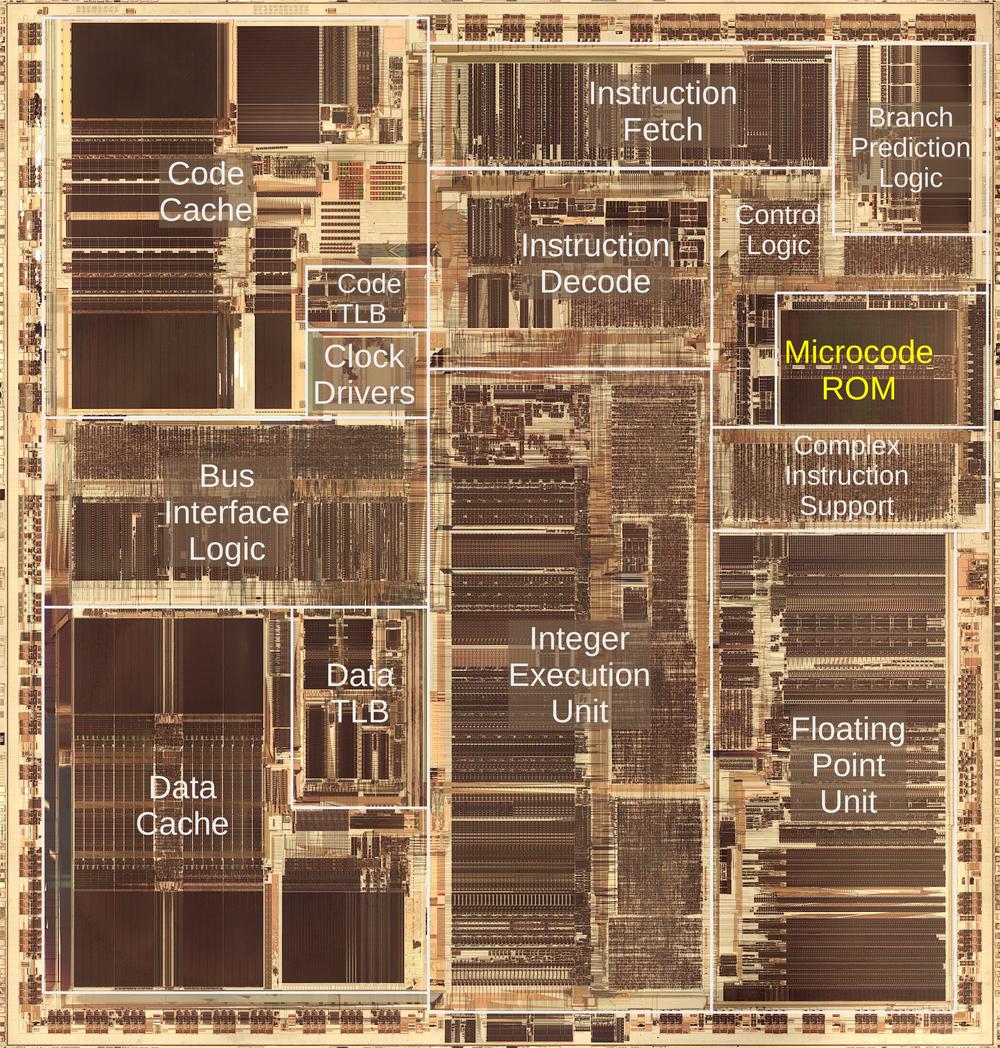
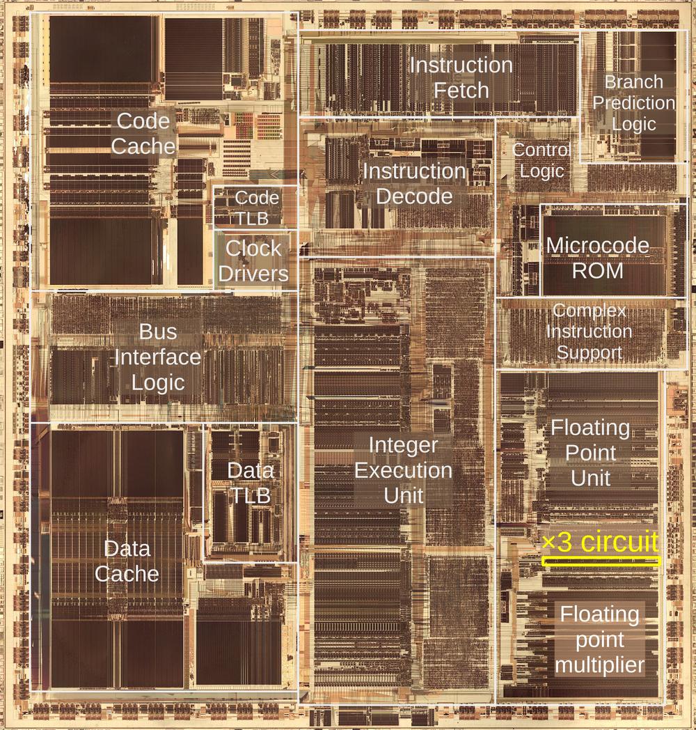
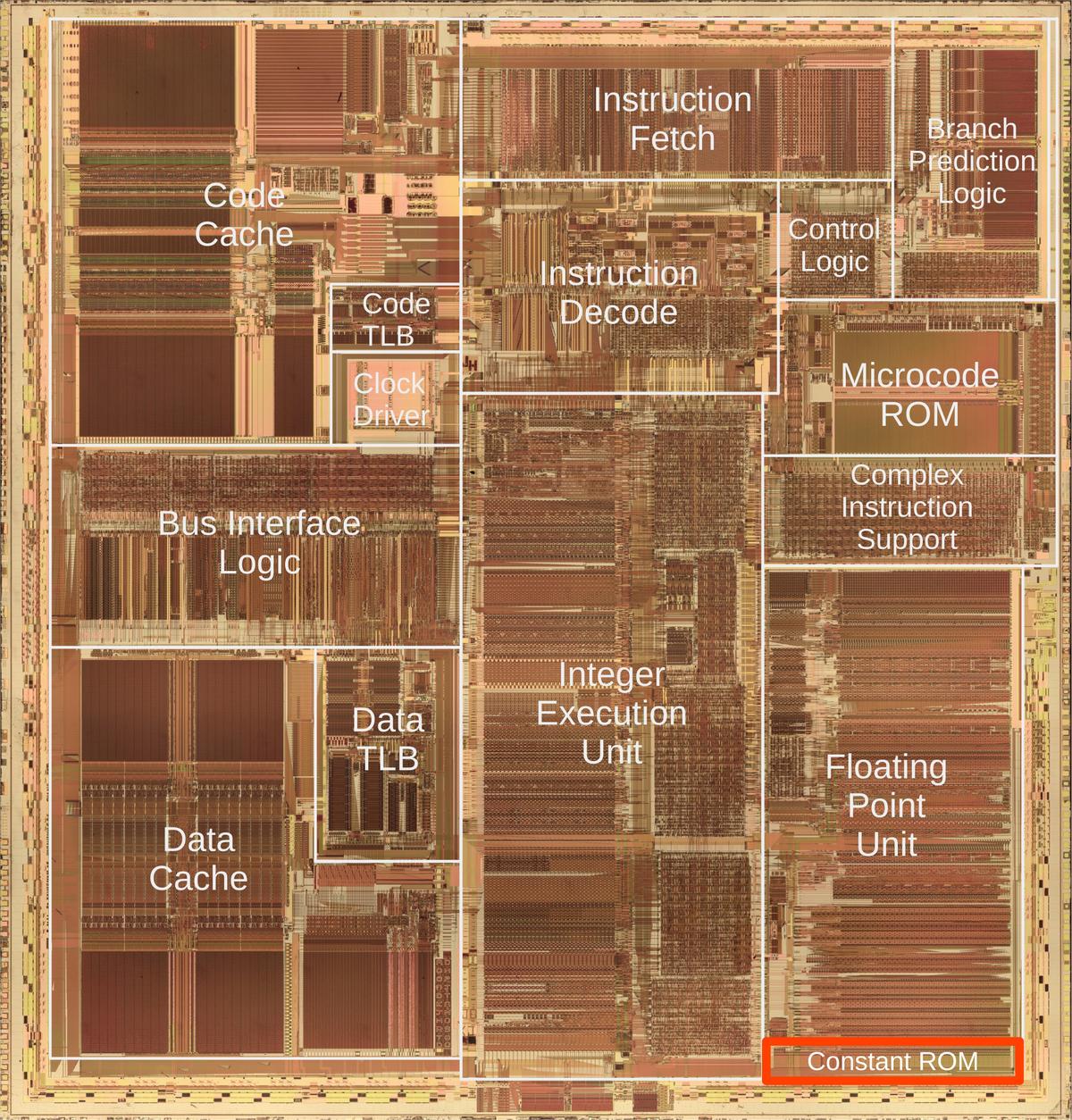
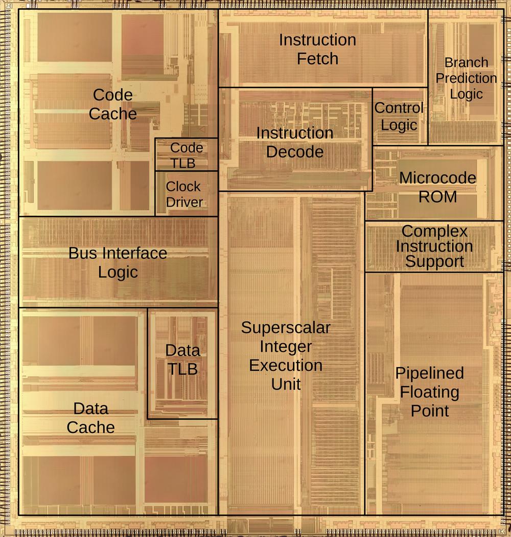
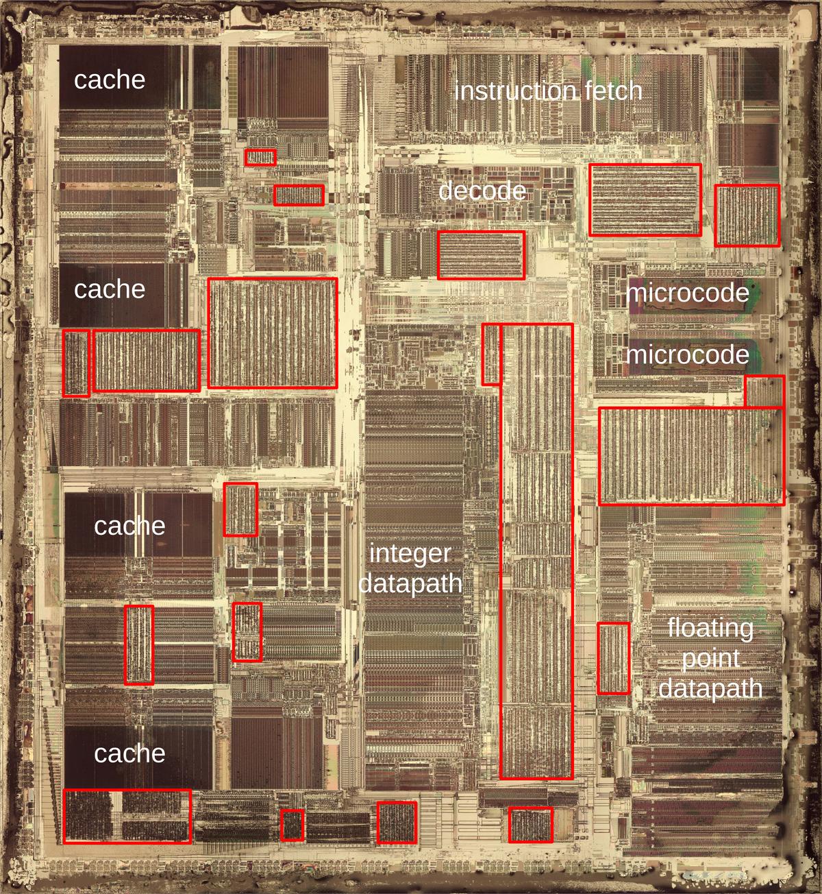
The photo below shows the Pentium's thumbnail-sized silicon die under a microscope. I've labeled the main functional blocks; the floating point unit is in the lower right with the constant ROM highlighted at the bottom. The various parts of the floating point unit form horizontal stripes. Data buses run vertically through the floating point unit, moving values around the unit.

Die photo of the Intel Pentium processor with the floating point constant ROM highlighted in red. Click this image (or any other) for a larger version.

Die photo of the Intel Pentium processor with the floating point constant ROM highlighted in red. Click this image (or any other) for a larger version.

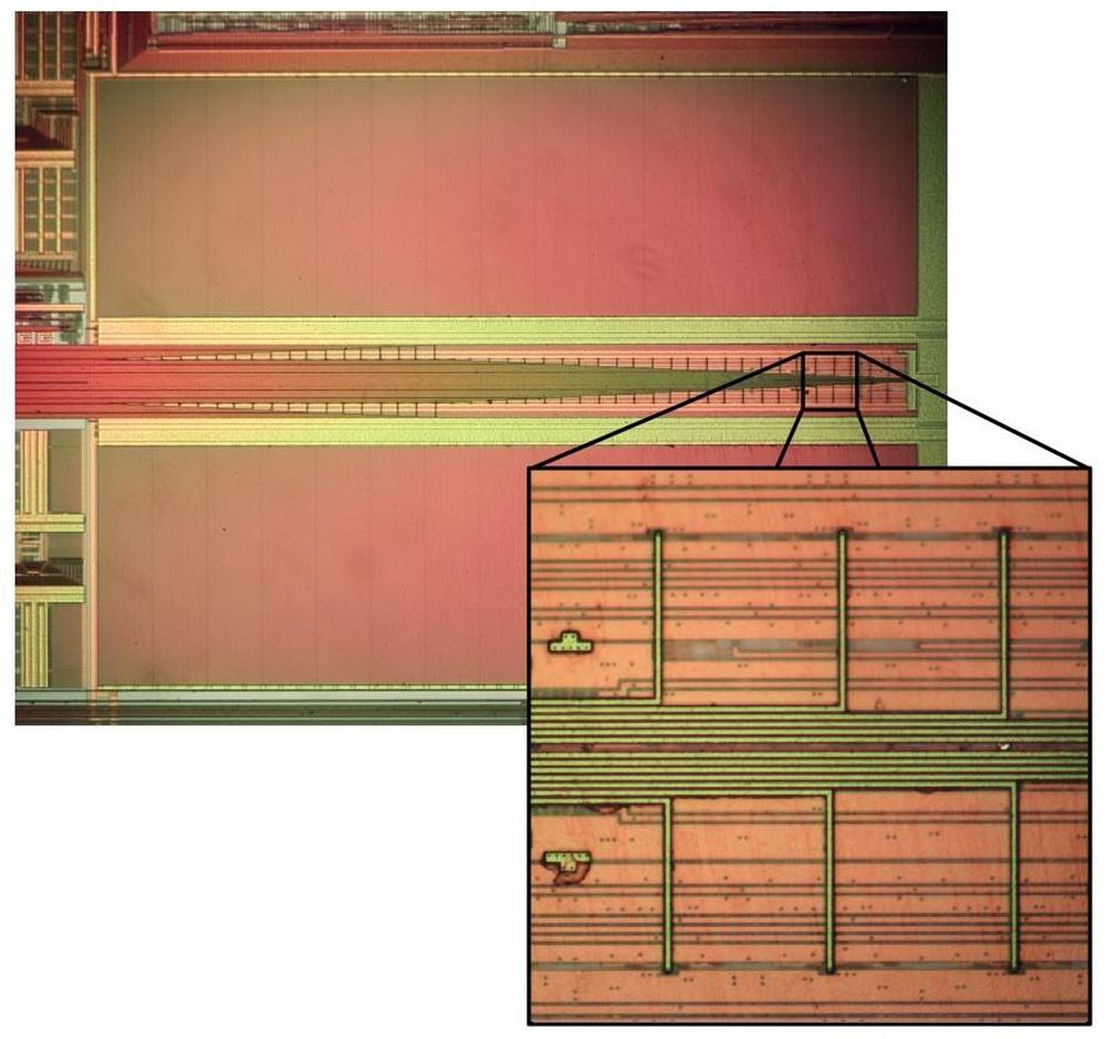
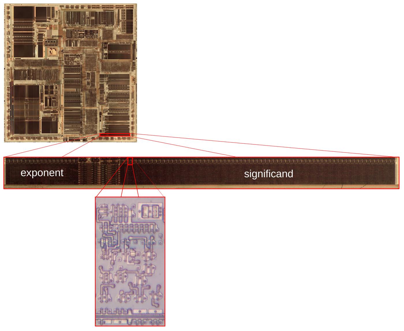
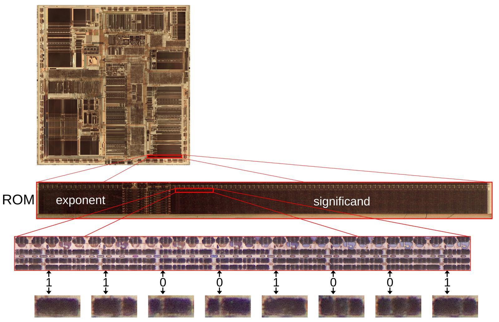
The diagram below shows how the circuitry in this post forms part of the Pentium. Zooming in to the bottom of the chip shows the constant ROM, holding 86-bit words: at the left, the exponent section provides 18 bits. At the right, the wider significand section provides 68 bits. Below that, the diagram zooms in on the subject of this article: one of the 86 identical multiplexer/driver circuits that provides the output from the ROM. As you can see, this circuit is a microscopic speck in the chip.

Zooming in on the constant ROM's driver circuits at the top of the ROM.

Zooming in on the constant ROM's driver circuits at the top of the ROM.

The layers

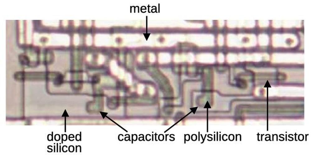
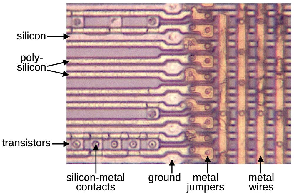
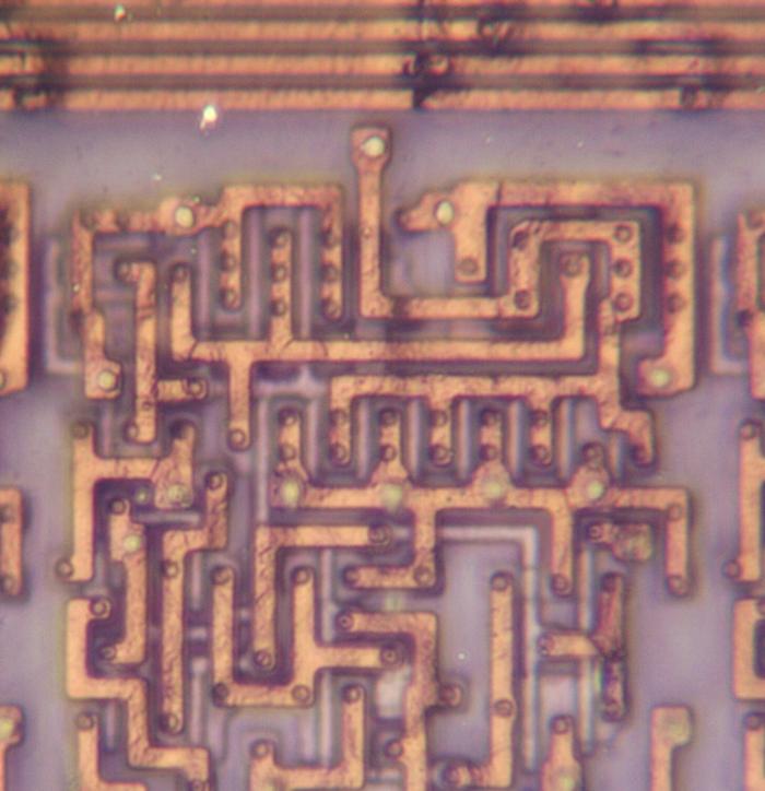
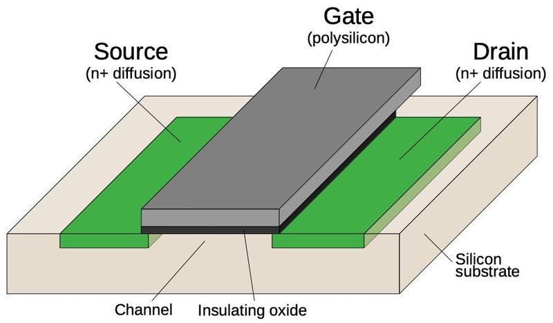
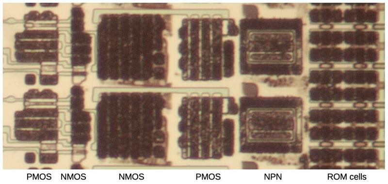
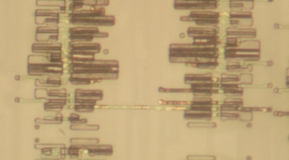
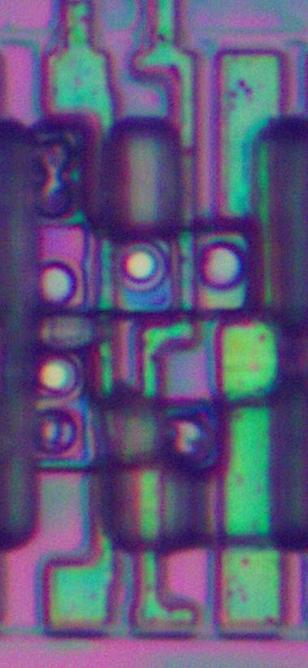
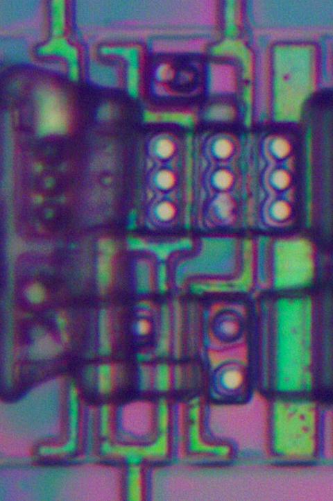
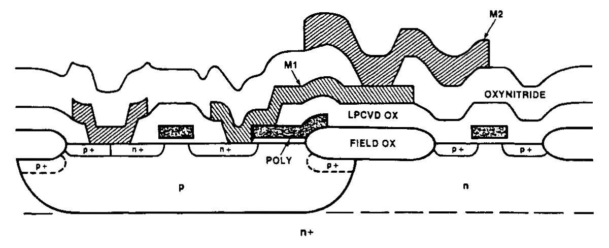
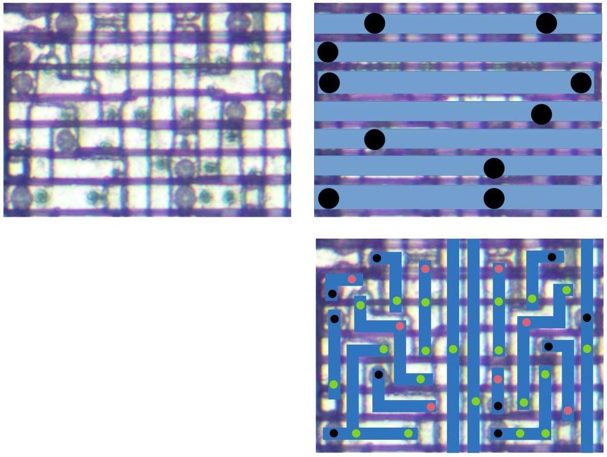
In this section, I'll show how the Pentium is constructed from layers. The bottom layer of the chip consists of transistors fabricated on the silicon die. Regions of silicon are doped with impurities to change the electrical properties; these regions appear pinkish in the photo below, compared to the grayish undoped silicon. Thin polysilicon wiring is formed on top of the silicon. Where a polysilicon line crosses doped silicon, a transistor is formed; the polysilicon creates the transistor's gate. Most of these transistors are NMOS and PMOS transistors, but there is a bipolar transistor near the upper right, the large box-like structure. The dark circles are contacts, regions where the metal layer above is connected to the polysilicon or silicon to wire the circuits together.

The polysilicon and silicon layers form the Pentium's transistors. This photo shows part of the complete circuit.

The polysilicon and silicon layers form the Pentium's transistors. This photo shows part of the complete circuit.

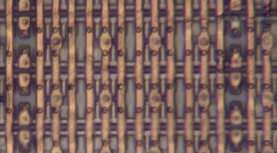
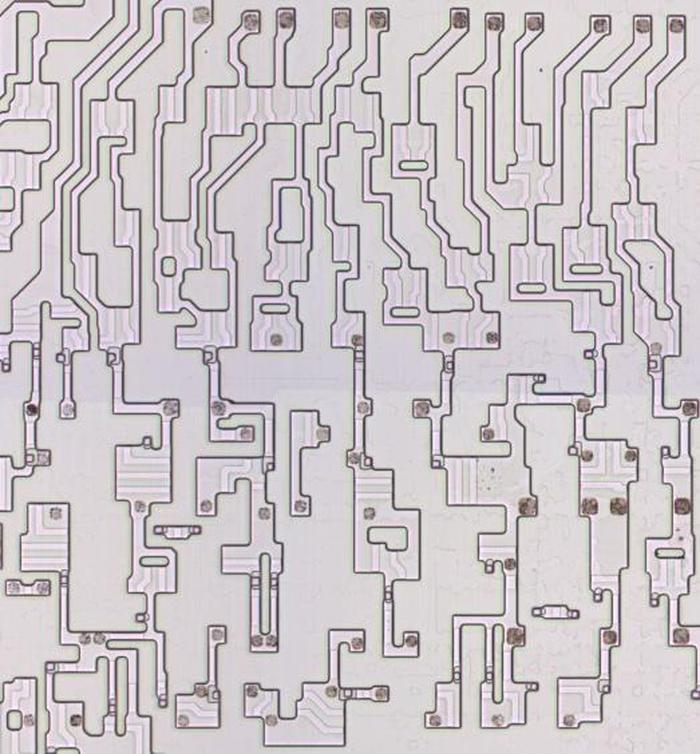
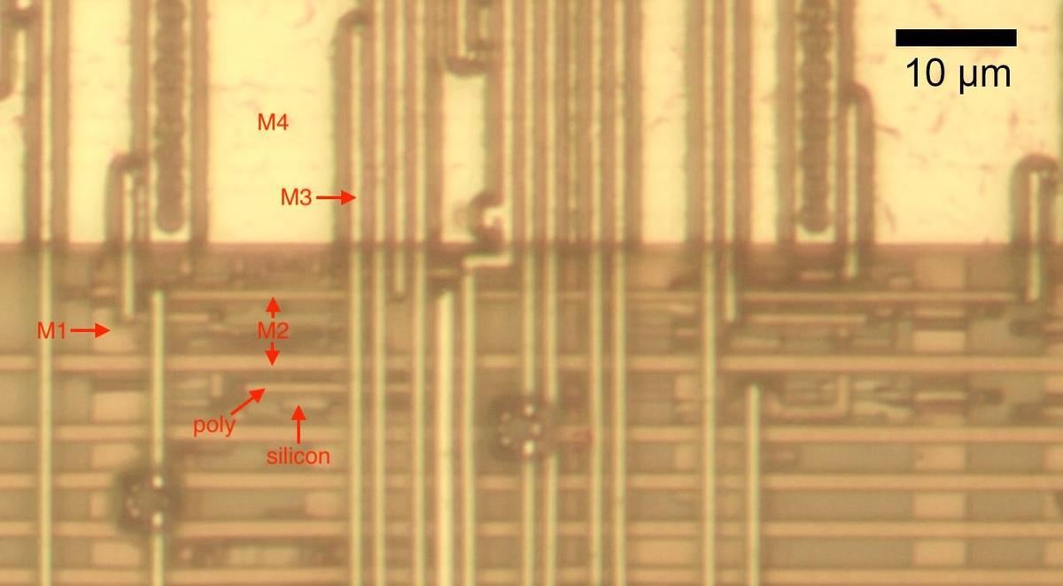
The Pentium has three layers of metal wiring. The photo below shows the bottom layer, called M1. For the most part, this layer of metal connects the transistors into various circuits, providing wiring over a short distance. The photos in this section show the same region of the chip, so you can match up features between the photos. For instance, the contacts below (black circles) match the black circles above, showing how this metal layer connects to the silicon and polysilicon circuits. You can see some of the silicon and polysilicon in this image, but most of it is hidden by the metal.

The Pentium's M1 metal layer is the bottom metal layer.

The Pentium's M1 metal layer is the bottom metal layer.

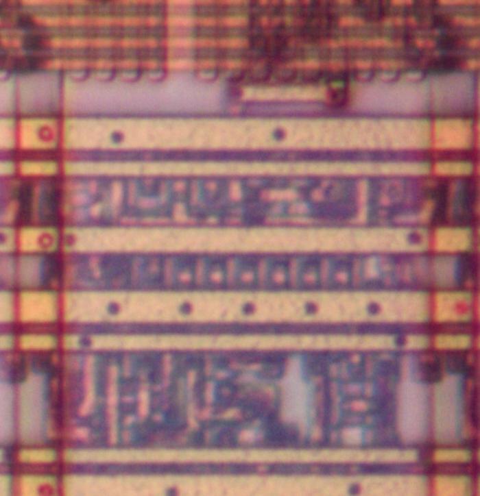
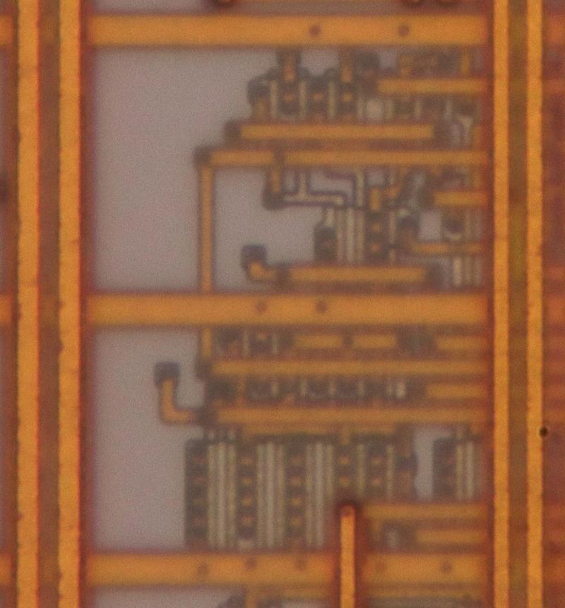
The M2 metal layer (below) sits above the M1 wiring. In this part of the chip, the M2 wires are horizontal. The thicker lines are power and ground. (Because they are thicker, they have lower resistance and can provide the necessary current to the underlying circuitry.) The thinner lines are control signals. The floating point unit is structured so functional blocks are horizontal, while data is transmitted vertically. Thus, a horizontal wire can supply a control signal to all the bits in a functional block.

The Pentium's M2 layer.

The Pentium's M2 layer.

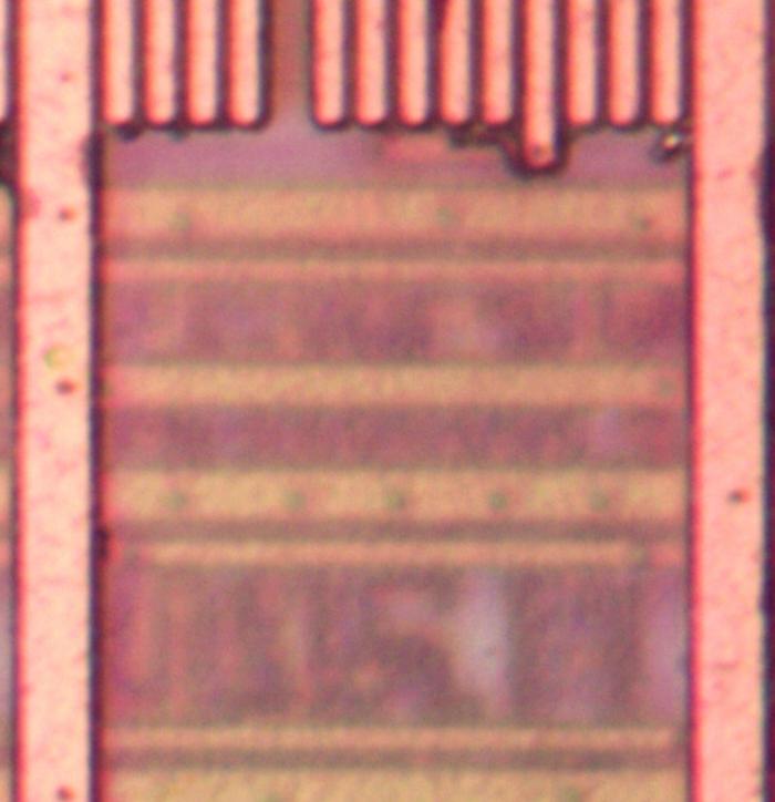
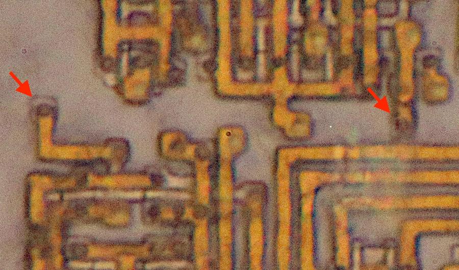
The M3 layer is the top metal layer in the Pentium. It is thicker, so it is better suited for the chip's main power and ground lines as well as long-distance bus wiring. In the photo below, the wide line on the left provides power, while the wide line on the right provides ground. The power and ground are distributed through wiring in the M2 and M1 layers until they are connected to the underlying transistors. At the top of the photo, vertical bus lines are visible; these extend for long distances through the floating point unit. Notice the slightly longer line, fourth from the right. This line provides one bit of data from the ROM, provided by the circuitry described below. The dot near the bottom is a via, connecting this line to a short wire in M2, connected to a wire in M1, connected to the silicon of the output transistors.

The Pentium's M3 metal layer. Lower layers are visible, but blurry due to the insulating oxide layers.

The Pentium's M3 metal layer. Lower layers are visible, but blurry due to the insulating oxide layers.

The circuits for the ROM's output

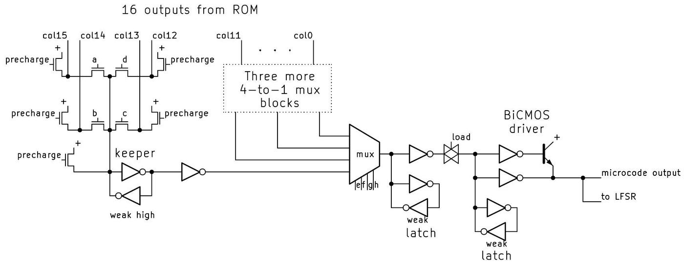
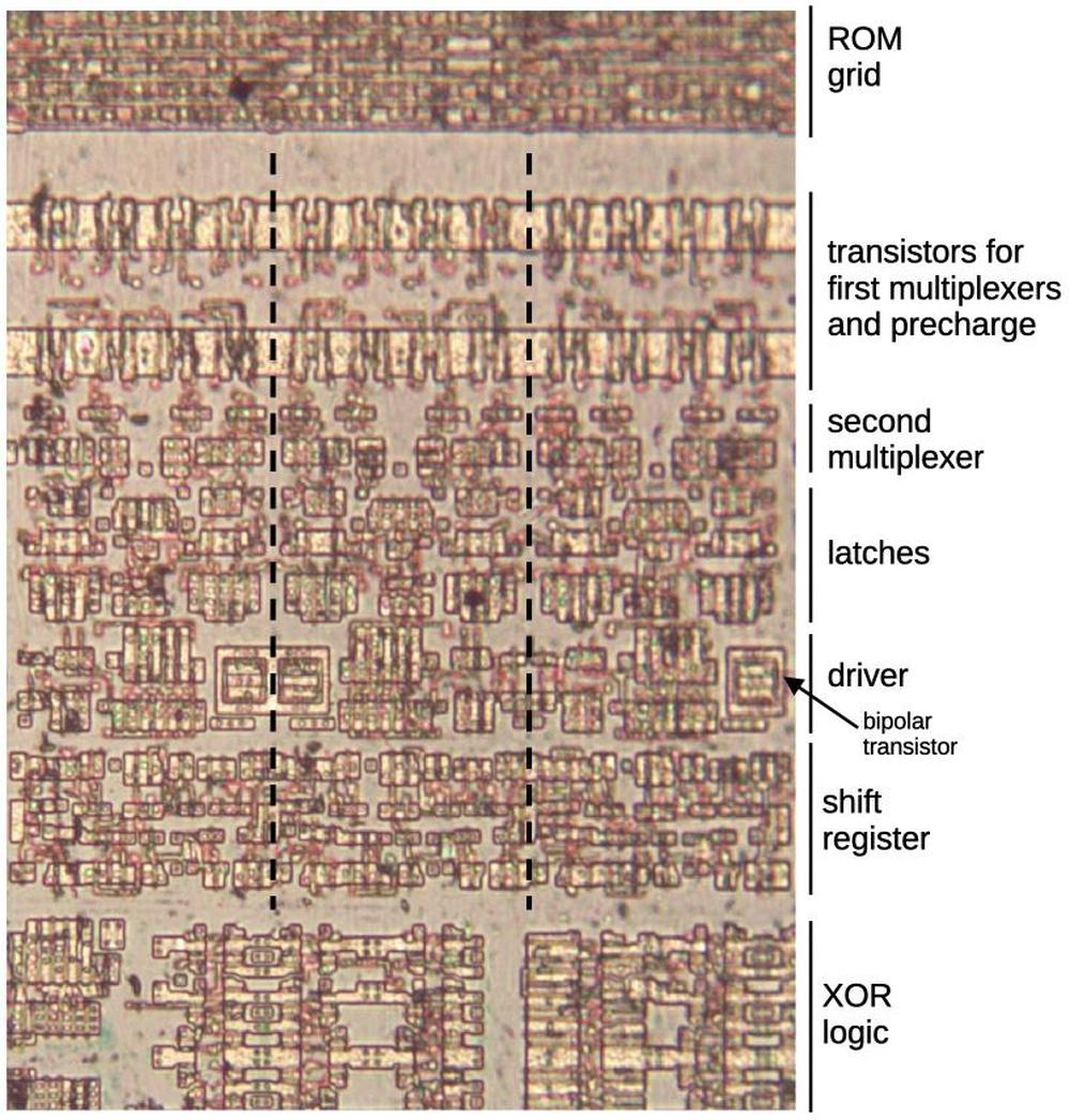
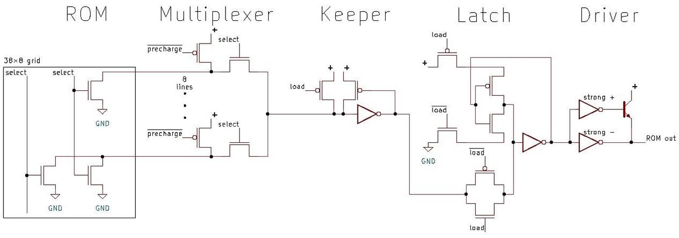
The simplified schematic below shows the circuit that I reverse-engineered. This circuit is repeated 86 times, once for each bit in the ROM's word. You might expect the ROM to provide a single 86-bit word. However, to make the layout work better, the ROM provides eight words in parallel. Thus, the circuitry must select one of the eight words with a multiplexer. In particular, each of the 86 circuits has an 8-to-1 multiplexer to select one bit out of the eight. This bit is then stored in a latch. Finally, a high-current driver amplifies the signal so it can be sent through a bus, traveling to a destination halfway across the floating point unit.

A high-level schematic of the circuit.

A high-level schematic of the circuit.

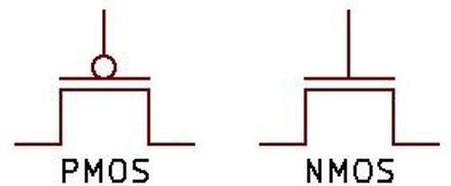
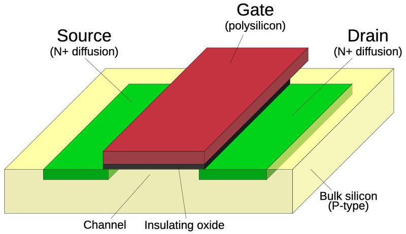
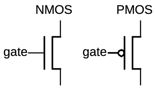
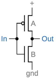
I'll provide a quick review of MOS transistors before I explain the circuitry in detail. CMOS circuitry uses two types of transistors—PMOS and NMOS—which are similar but also opposites. A PMOS transistor is turned on by a low signal on the gate, while an NMOS transistor is turned on by a high signal on the gate; the PMOS symbol has an inversion bubble on the gate. A PMOS transistor works best when pulling its output high, while an NMOS transistor works best when pulling its output low. CMOS circuitry normally uses the two types of MOS transistors in a Complementary fashion to implement logic gates, working together. What makes the circuits below interesting is that they often use NMOS and PMOS transistors independently.

The symbol for a PMOS transistor and an NMOS transistor.

The symbol for a PMOS transistor and an NMOS transistor.

The detailed schematic below shows the circuitry at the transistor and inverter level. I'll go through each of the components in the remainder of this post.

A detailed schematic of the circuit. Click for a larger version.

A detailed schematic of the circuit. Click for a larger version.

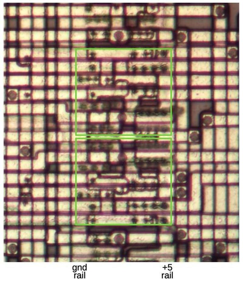
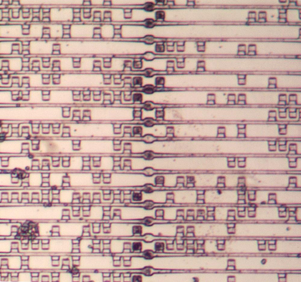
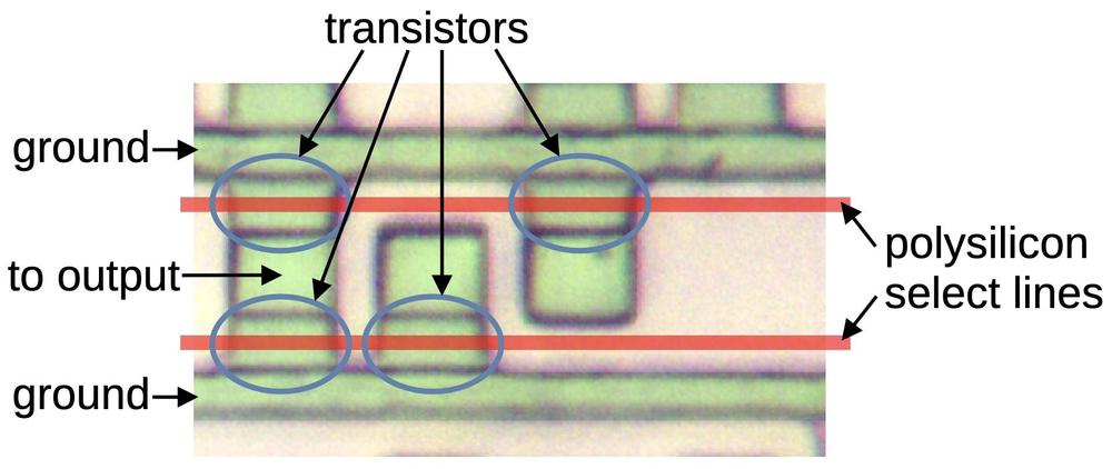
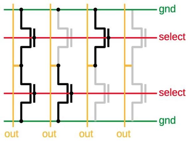
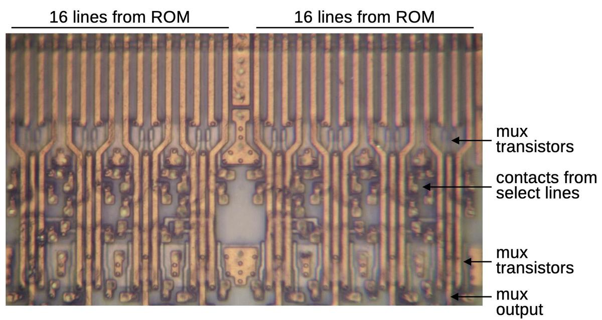
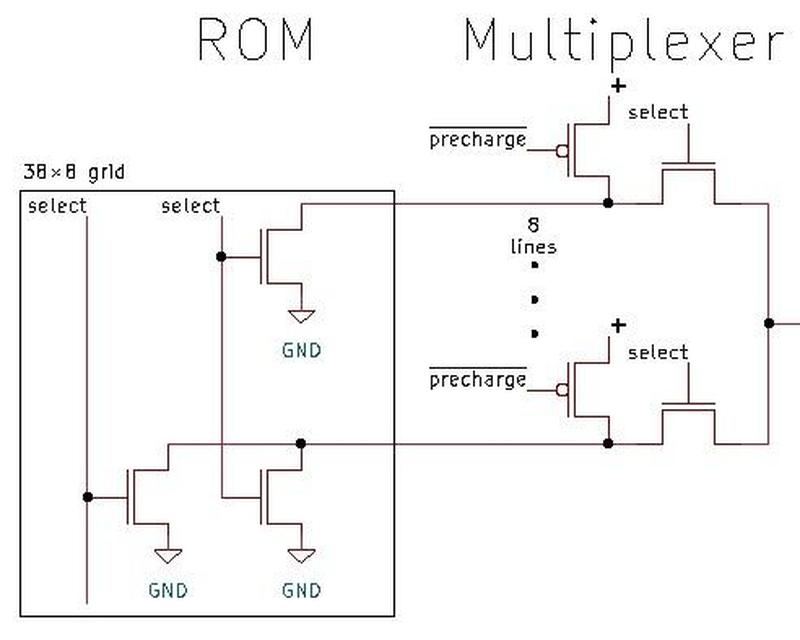
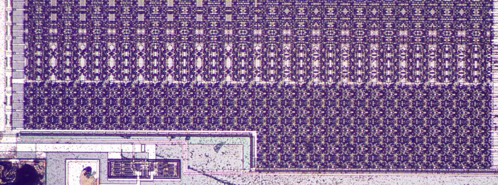
The ROM is constructed as a grid: at each grid point, the ROM can have a transistor for a 0 bit, or no transistor for a 1 bit. Thus, the data is represented by the transistor pattern. The ROM holds 304 constants so there are 304 potential transistors associated with each bit of the output word. These transistors are organized in a 38×8 grid. To select a word from the ROM, a select line activates one group of eight potential transistors. Each transistor is connected to ground, so the transistor (if present) will pull the associated line low, for a 0 bit. Note that the ROM itself consists of only NMOS transistors, making it half the size of a truly CMOS implementation. For more information on the structure and contents of the ROM, see my earlier article.

The ROM grid and multiplexer.

The ROM grid and multiplexer.

A ROM transistor can pull a line low for a 0 bit, but how does the line get pulled high for a 1 bit? This is accomplished by a precharge transistor on each line. Before a read from the ROM, the precharge transistors are all activated, pulling the lines high. If a ROM transistor is present on the line, the line will next be pulled low, but otherwise it will remain high due to the capacitance on the line.

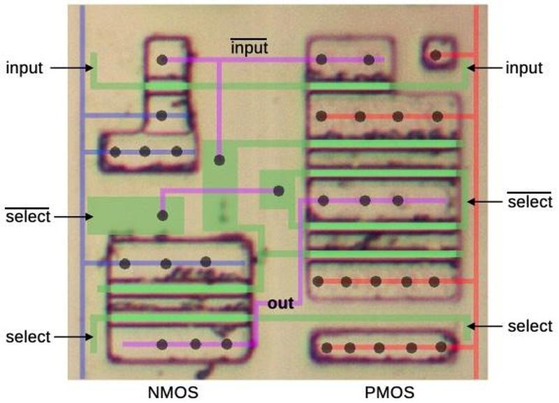
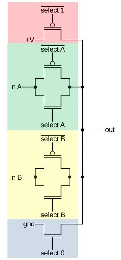
Next, the multiplexer above selects one of the 8 lines, depending on which word is being accessed. The multiplexer consists of eight transistors. One transistor is activated by a select line, allowing the ROM's signal to pass through. The other seven transistors are in the off state, blocking those ROM signals. Thus, the multiplexer selects one of the 8 bits from the ROM.

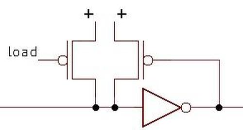
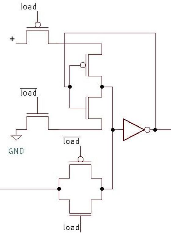
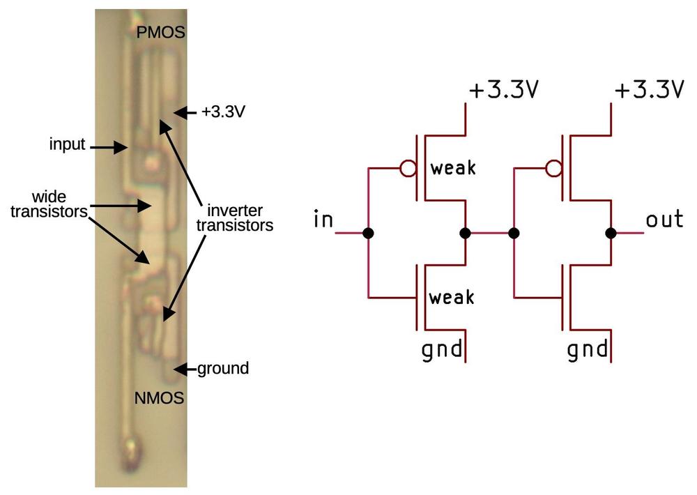
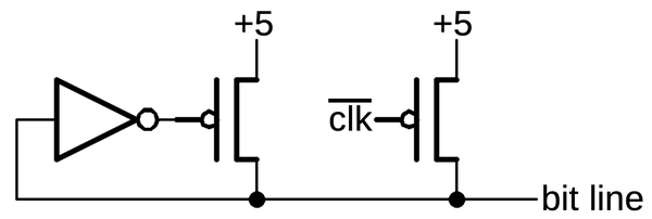
The circuit below is the "keeper." As explained above, each ROM line is charged high before reading the ROM. However, this charge can fade away. The job of the keeper is to keep the multiplexer's output high until it is pulled low. This is implemented by an inverter connected to a PMOS transistor. If the signal on the line is high, the PMOS transistor will turn on, pulling the line high. (Note that a PMOS transistor is turned on by a low signal, thus the inverter.) If the ROM pulls the line low, the transistor will turn off and stop pulling the line high. This transistor is very weak, so it is easily overpowered by the signal from the ROM. The transistor on the left ensures that the line is high at the start of the cycle.

The keeper circuit.

The keeper circuit.

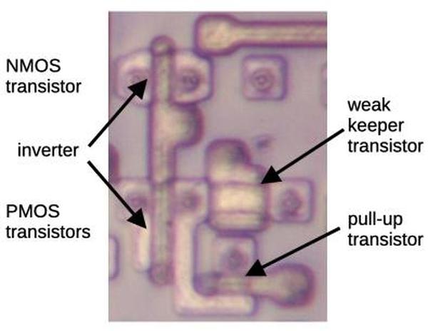
The diagram below shows the transistors for the keeper. The two transistors on the left implement a standard CMOS inverter. On the right, note the weak transistor that holds the line high. You might notice that the weak transistor looks larger and wonder why that makes the transistor weak rather than strong. The explanation is that the transistor is large in the "wrong" dimension. The current capacity of an MOS transistor is proportional to the width/length ratio of its gate. (Width is usually the long dimension and length is usually the skinny dimension.) The weak transistor's length is much larger than the other transistors, so the W/L ratio is smaller and the transistor is weaker. (You can think of the transistor's gate as a bridge between its two sides. A wide bridge with many lanes lets lots of traffic through. However, a long, single-lane bridge will slow down the traffic.)

The silicon implementation of the keeper.

The silicon implementation of the keeper.

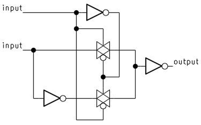
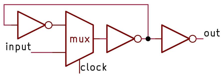
Next, we come to the latch, which remembers the value read from the ROM. This latch will read its input when the load signal is high. When the load signal goes low, the latch will hold its value. Conceptually, the latch is implemented with the circuit below. A multiplexer selects the lower input when the load signal is active, passing the latch input through to the (inverted) output. But when the load signal goes low, the multiplexer will select the top input, which is feedback of the value in the latch. This signal will cycle through the inverters and the multiplexer, holding the value until a new value is loaded. The inverters are required because the multiplexer itself doesn't provide any amplification; the signal would rapidly die out if not amplified by the inverters.

The implementation of the latch.

The implementation of the latch.

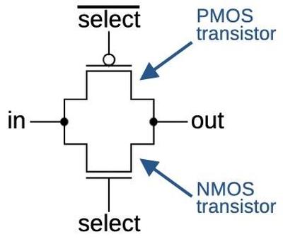
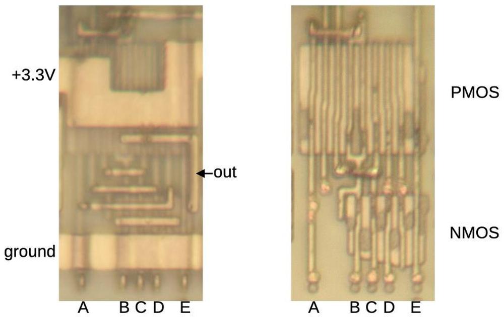
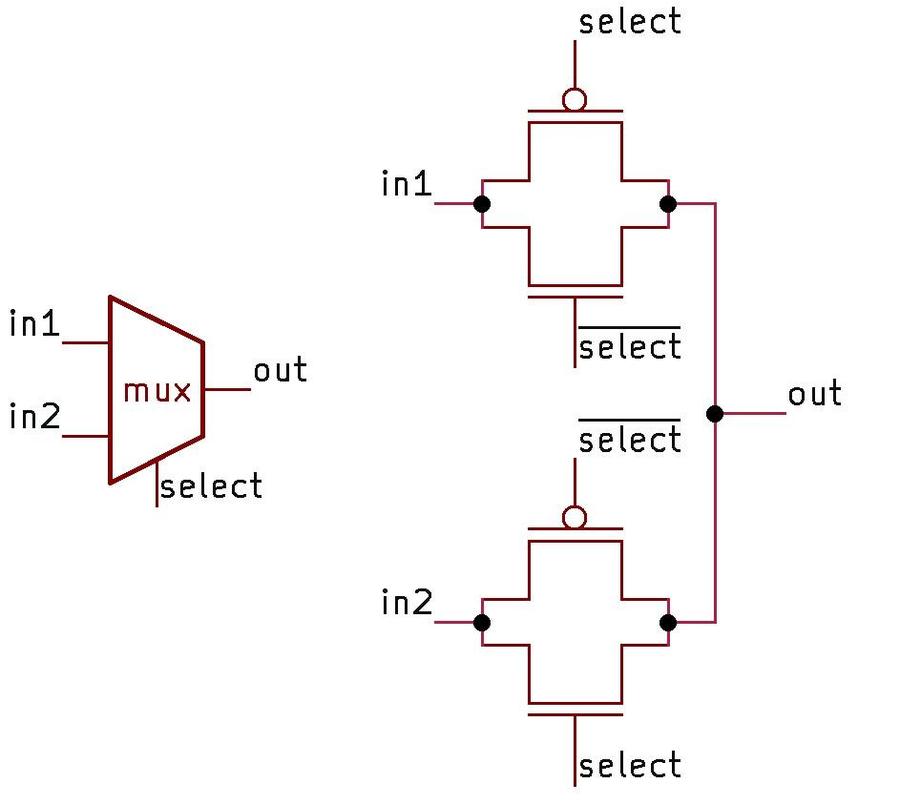
The multiplexer is implemented with two CMOS switches, one to select each multiplexer input. Each switch is a pair of PMOS and NMOS transistors that turn on together, allowing a signal to pass through. (See the bottom two transistors below.)1 The upper circuit is trickier. Conceptually, it is an inverter feeding into the multiplexer's CMOS switch. However, the order is switched so the switch feeds into the inverter. The result is not-exactly-a-switch and not-exactly-an-inverter, but the result is the same. You can also view it as an inverter with power and ground that gets cut off when not selected. I suspect this implementation uses slightly less power than the straightforward implementation.

The detailed schematic of the latch.

The detailed schematic of the latch.

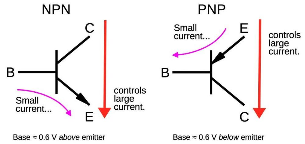
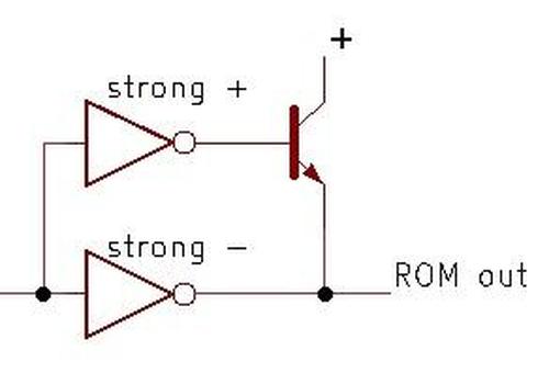
The most unusual circuit is the BiCMOS driver. By adding a few extra processing steps to the regular CMOS manufacturing process, bipolar (NPN and PNP) transistors can be created. The Pentium extensively used BiCMOS circuits since they reduced signal delays by up to 35%. Intel also used BiCMOS for the Pentium Pro, Pentium II, Pentium III, and Xeon processors. However, as chip voltages dropped, the benefit from bipolar transistors dropped too and BiCMOS was eventually abandoned.

The BiCMOS driver circuit.

The BiCMOS driver circuit.

In the Pentium, BiCMOS drivers are used when signals must travel a long distance across the chip. (In this case, the ROM output travels about halfway up the floating point unit.) These long wires have a lot of capacitance so a high-current driver circuit is needed and the NPN transistor provides extra "oomph."

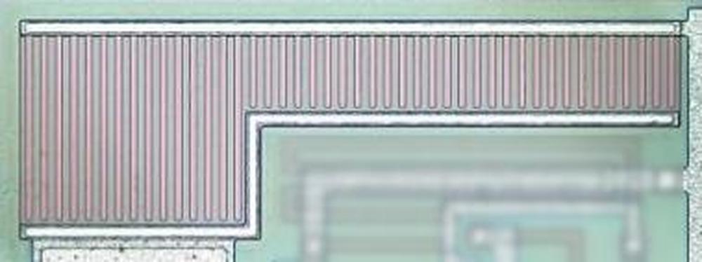
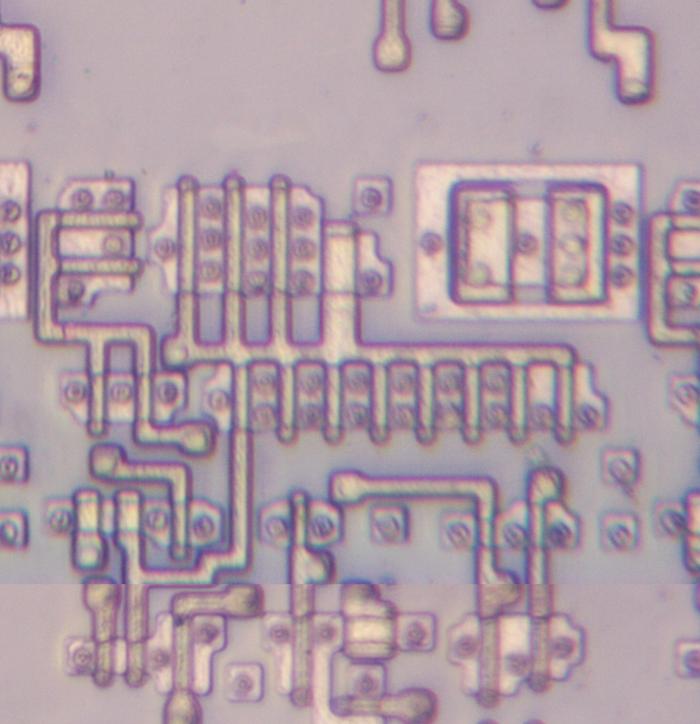
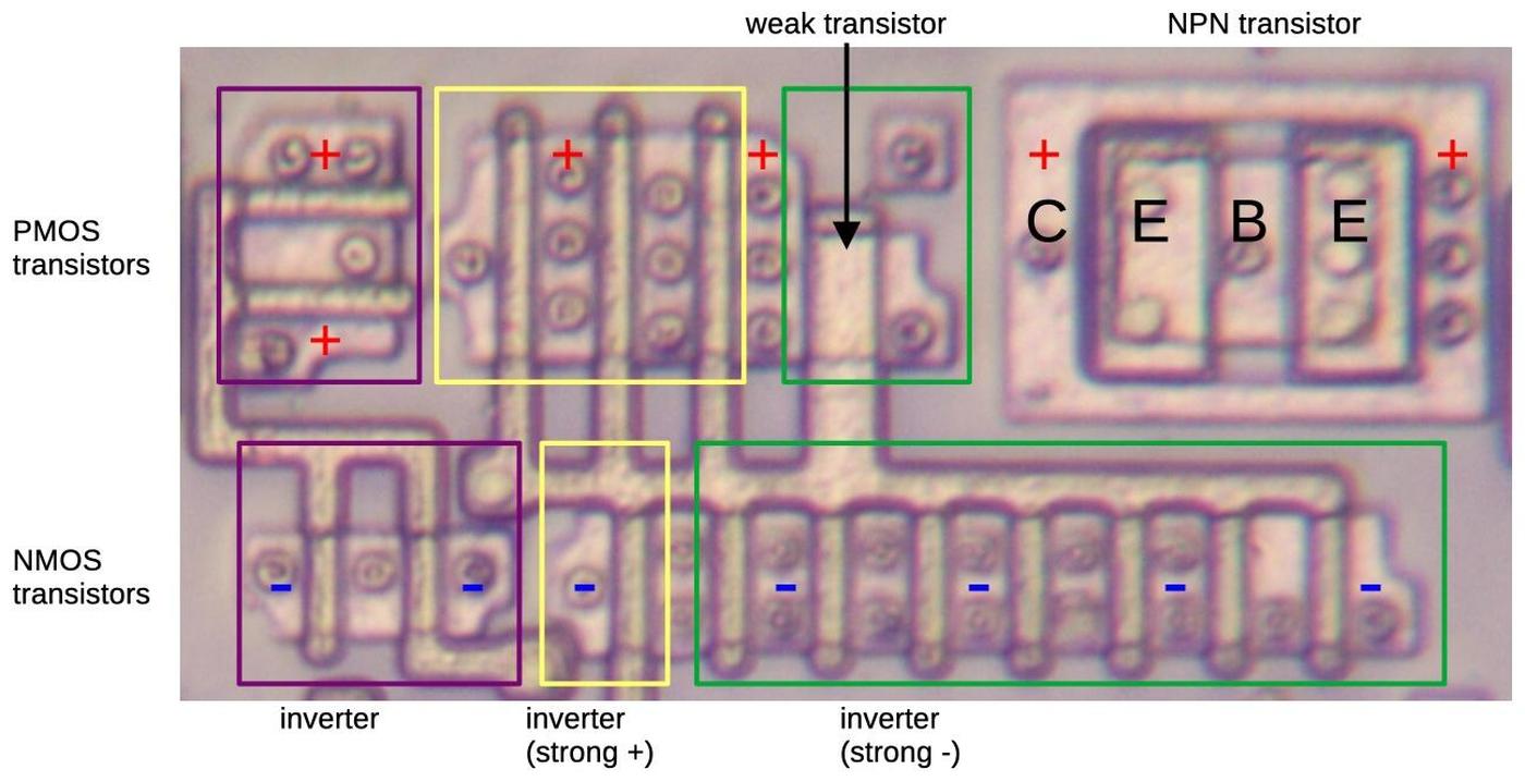
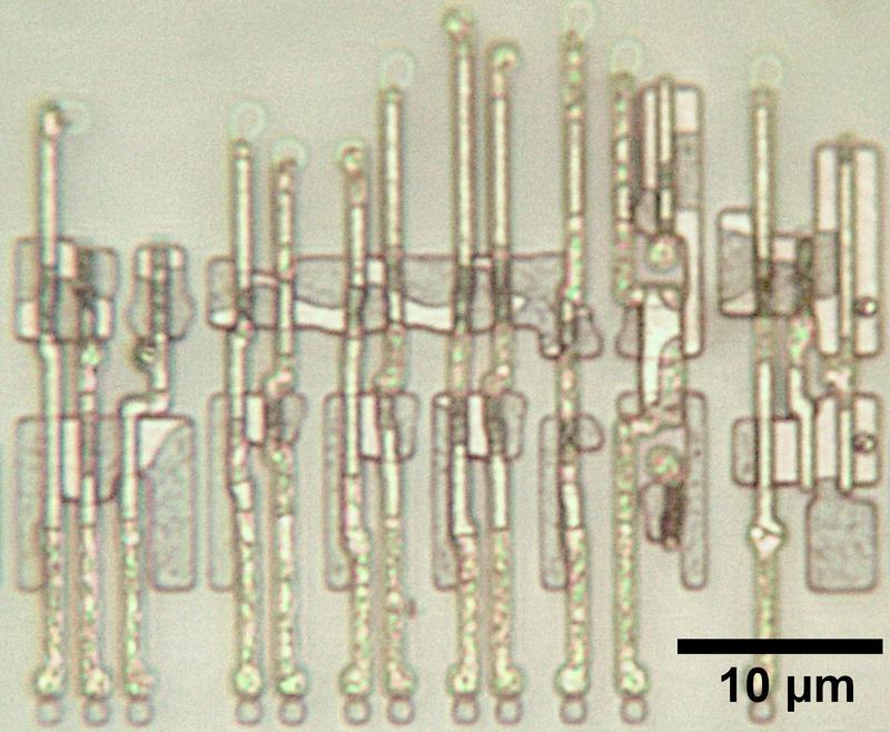
The diagram below shows how the driver is implemented. The NPN transistor is the large boxy structure in the upper right. When the base (B) is pulled high, current flows from the collector (C), pulling the emitter (E) high and thus rapidly pulling the output high. The remainder of the circuit consists of three inverters, each composed of PMOS and NMOS transistors. When a polysilicon line crosses doped silicon, it creates a transistor gate, so each crossing corresponds to a transistor. The inverters use multiple transistors in parallel to provide more current; the transistor sources and/or drains overlap to make the circuitry more compact.

This diagram shows the silicon and polysilicon for the driver circuit.

This diagram shows the silicon and polysilicon for the driver circuit.

One interesting thing about this circuit is that each inverter is carefully designed to provide the desired current, with a different current for a high output versus a low output. The first transistor (purple boxes) has two PMOS transistors and two NMOS transistors, so it is a regular inverter, balanced for high and low outputs. (This inverter is conceptually part of the latch.) The second inverter (yellow boxes) has three large PMOS transistors and one smaller NMOS transistor, so it has more ability to pull the output high than low. This transistor turns on the NPN transistor by providing a high signal to the base, so it needs more current in the high state. The third inverter (green boxes) has one weak PMOS transistor and seven NMOS transistors, so it can pull its output low strongly, but can barely pull its output high. This transistor pulls the ROM output line low, so it needs enough current to drive the entire bus line. But this transistor doesn't need to pull the output high—that's the job of the NPN transistor—so the PMOS transistor can be weak. The construction of the weak transistor is similar to the keeper's weak transistor; its gate length is much larger than the other transistors, so it provides less current.

Conclusions

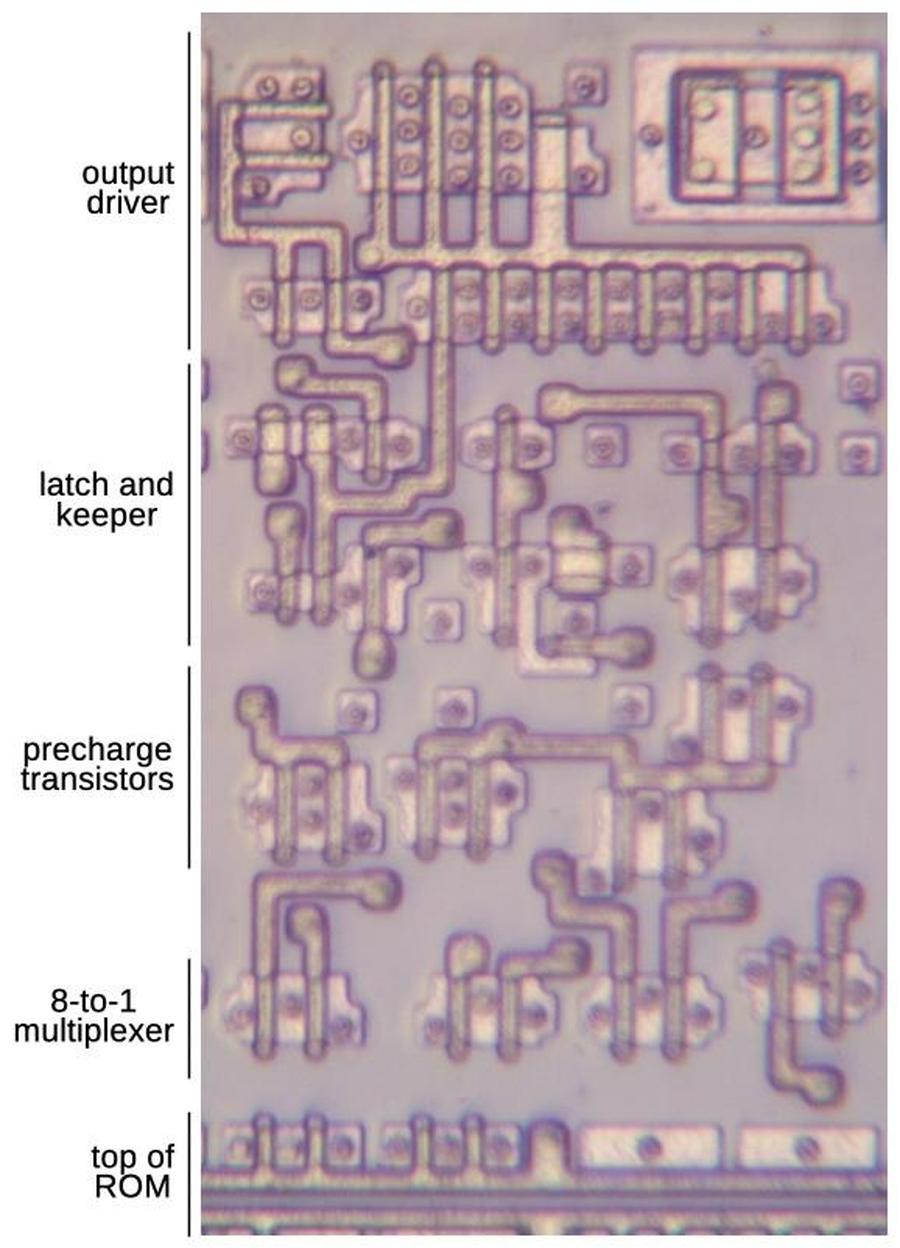
The diagram below shows how the functional blocks are arranged in the complete circuit, from the ROM at the bottom to the output at the top. The floating point unit is constructed with a constant width for each bit—38.5 µm—so the circuitry is designed to fit into this width. The layout of this circuitry was hand-optimized to fit as tightly as possible, In comparison, much of the Pentium's circuitry was arranged by software using a standard-cell approach, which is much easier to design but not as dense. Since each bit in the floating point unit is repeated many times, hand-optimization paid off here.

The silicon and polysilicon of the circuit, showing the functional blocks.

The silicon and polysilicon of the circuit, showing the functional blocks.

This circuit contains 47 transistors. Since it is duplicated once for each bit, it has 4042 transistors in total, a tiny fraction of the Pentium's 3.1 million transistors. In comparison, the MOS 6502 processor has about 3500-4500 transistors, depending on how you count. In other words, the circuit to select a word from the Pentium's ROM is about as complex as the entire 6502 processor. This illustrates the dramatic growth in processor complexity described by Moore's law.

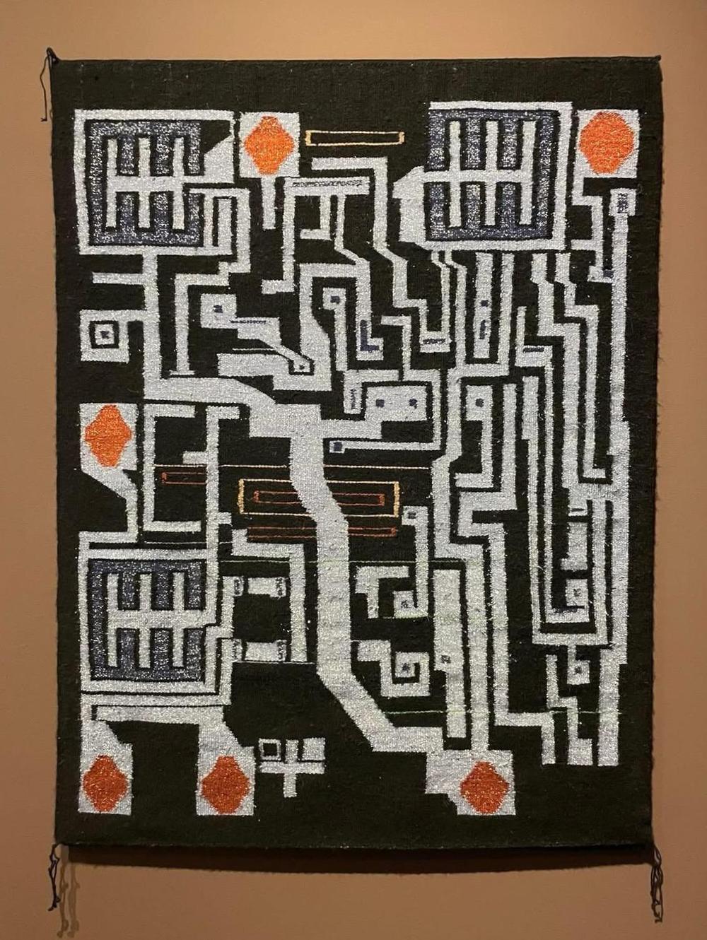
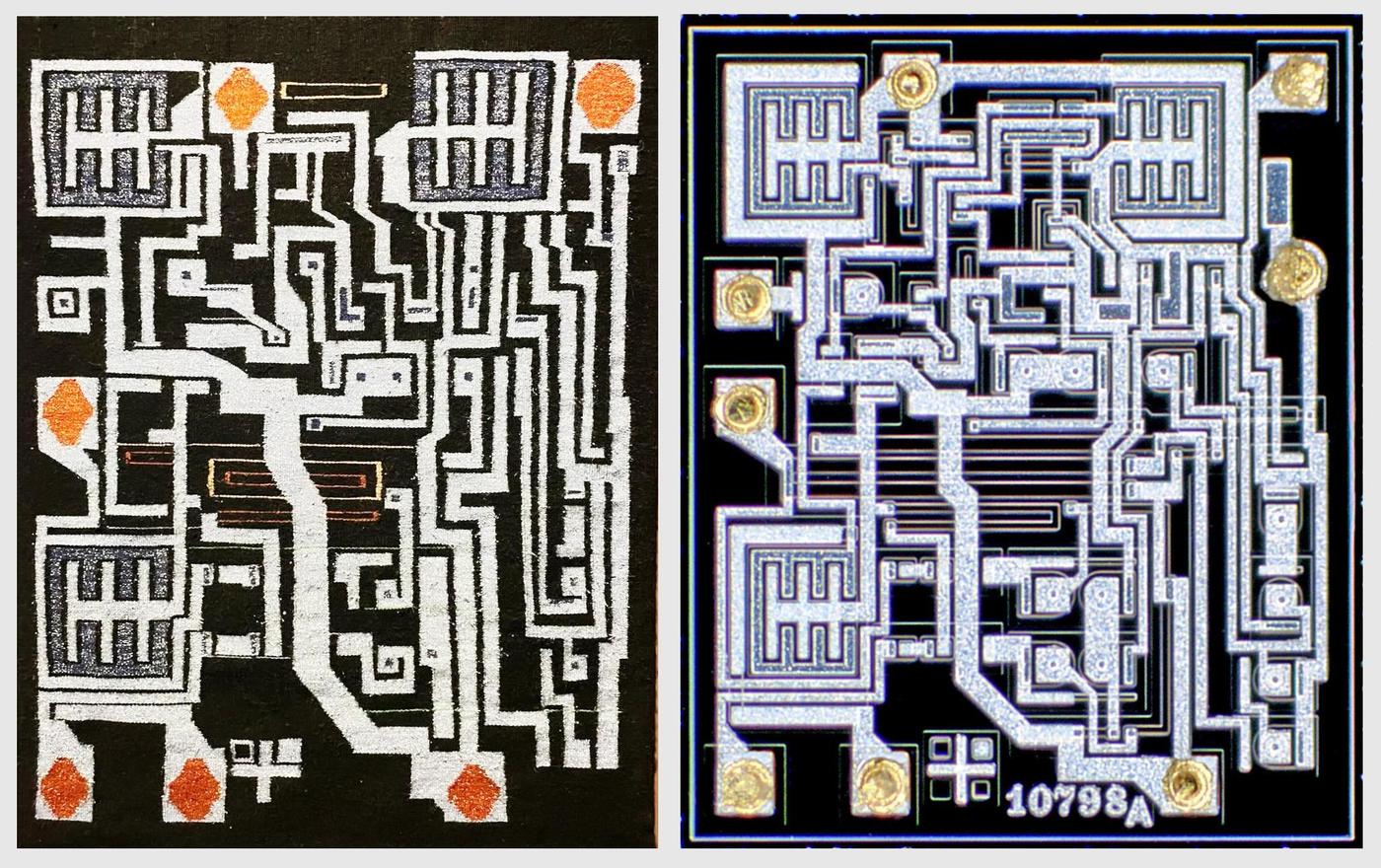
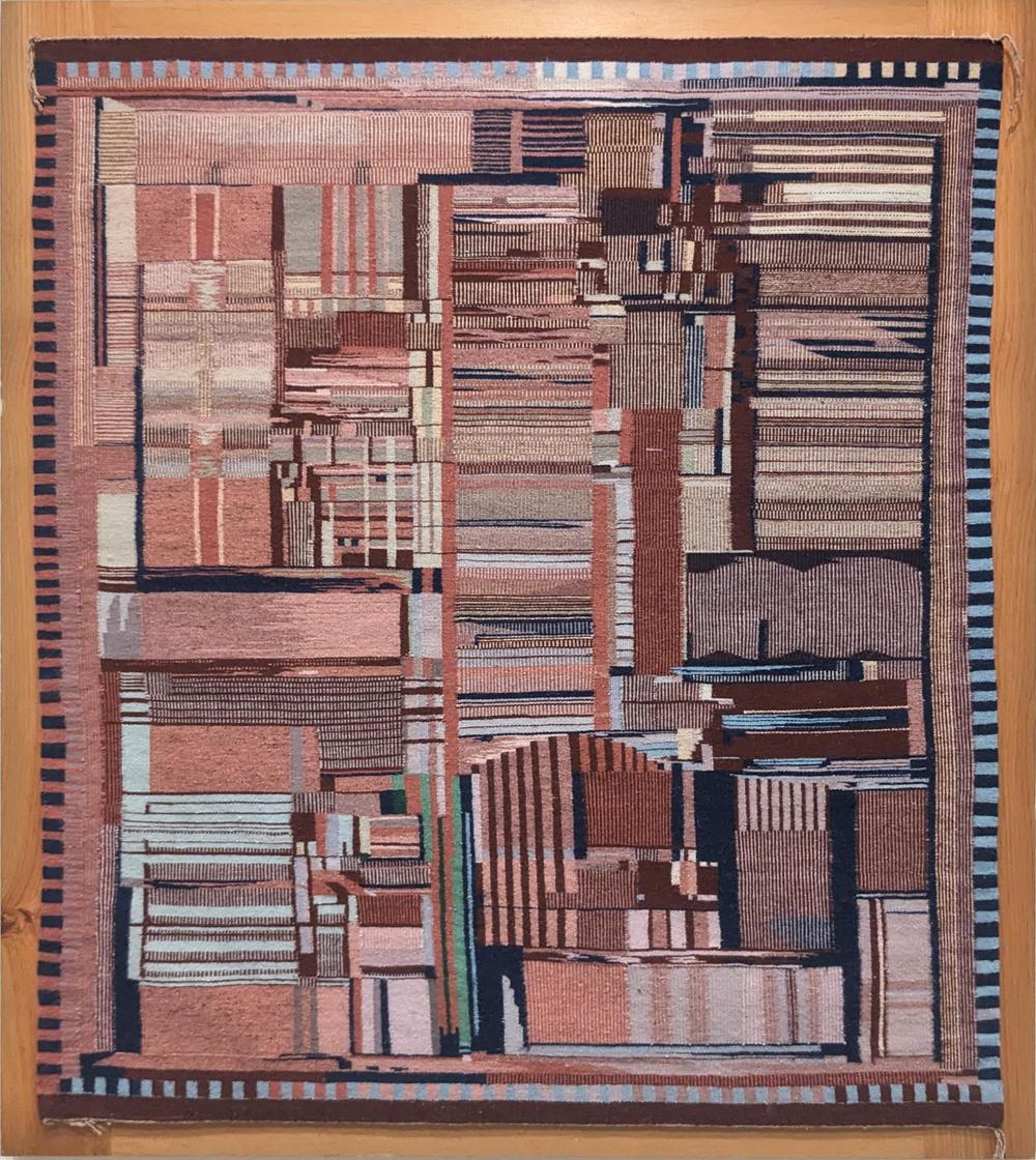
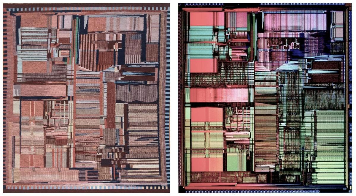
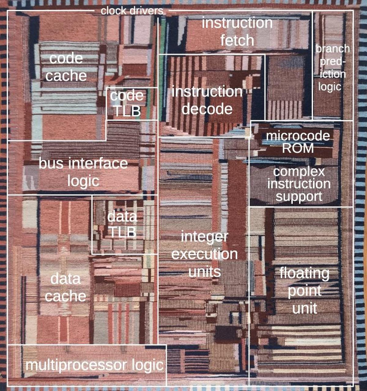
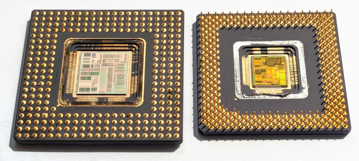
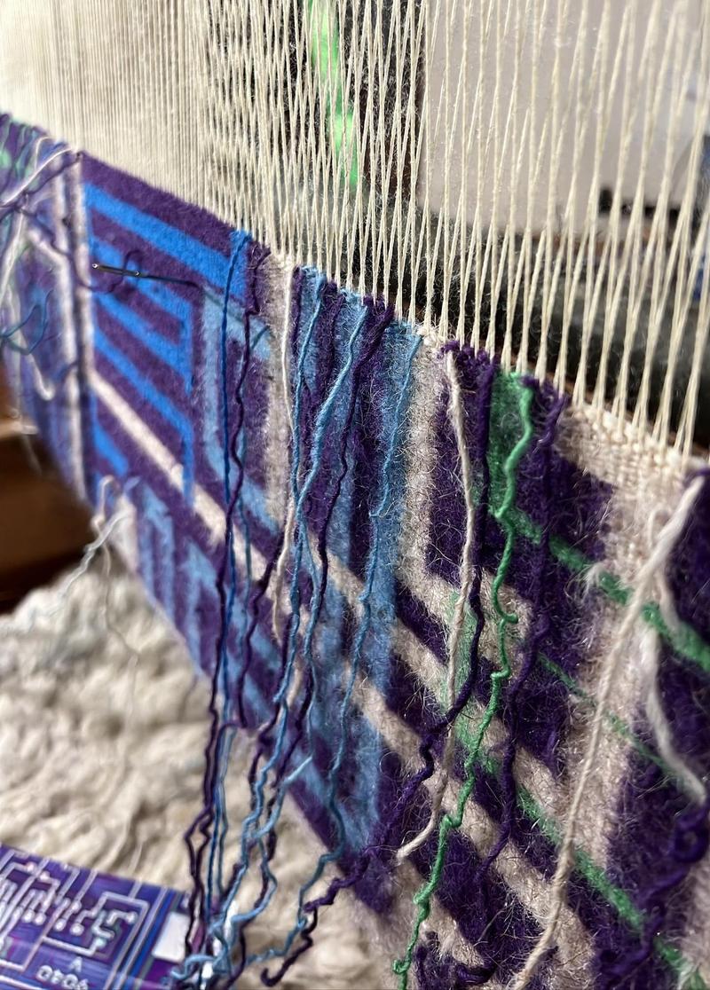
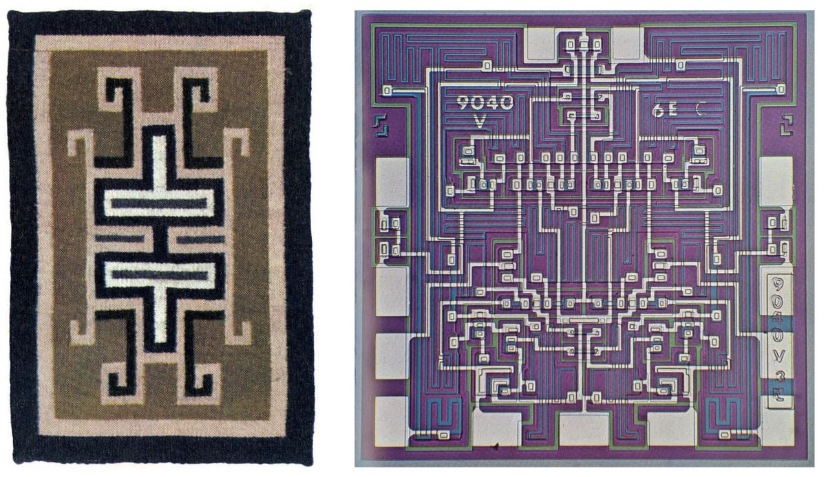
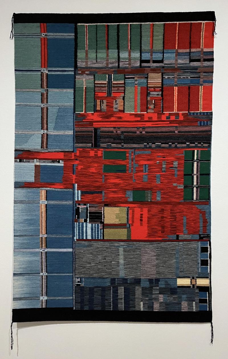
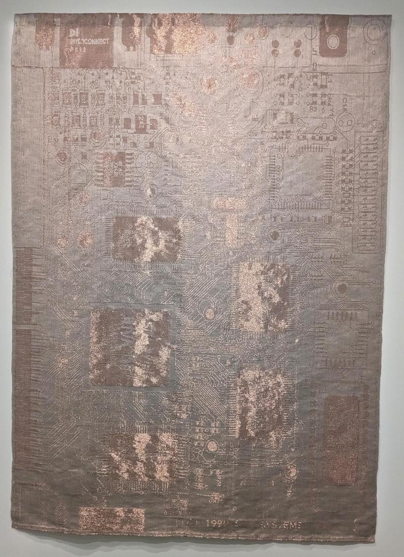
I plan to write more about the Pentium so follow me on Bluesky (@righto.com) or RSS for updates. (I'm no longer on Twitter.) You might enjoy reading about the Pentium Navajo rug.

Notes

  1. The 8-to-1 multiplexer and the latch's multiplexer use different switch implementations: the first is built from NMOS transistors while the second is built from paired PMOS and NMOS transistors. The reason is that NMOS transistors are better at pulling signals low, while PMOS transistors are better at pulling signals high. Combining the transistors creates a switch that passes low and high signals efficiently, which is useful in the latch. The 8-to-1 multiplexer, however, only needs to pull signals low (due to the precharging), so the NMOS-only multiplexer works in this role. (Note that early NMOS processors like the 6502 and 8086 built multiplexers and pass-transistor logic out of solely NMOS. This illustrates that you can use NMOS-only switches with both logic levels, but performance is better if you add PMOS transistors.) 

Reverse-engineering a carry-lookahead adder in the Pentium

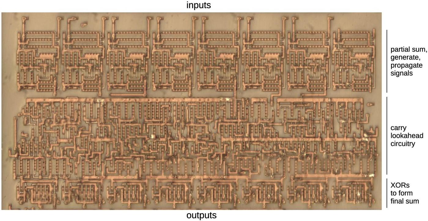
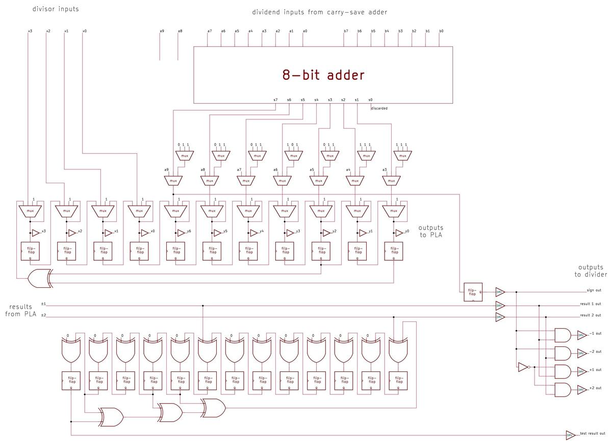
Addition is harder than you'd expect, at least for a computer. Computers use multiple types of adder circuits with different tradeoffs of size versus speed. In this article, I reverse-engineer an 8-bit adder in the Pentium's floating point unit. This adder turns out to be a carry-lookahead adder, in particular, a type known as "Kogge-Stone."1 In this article, I'll explain how a carry-lookahead adder works and I'll show how the Pentium implemented it. Warning: lots of Boolean logic ahead.

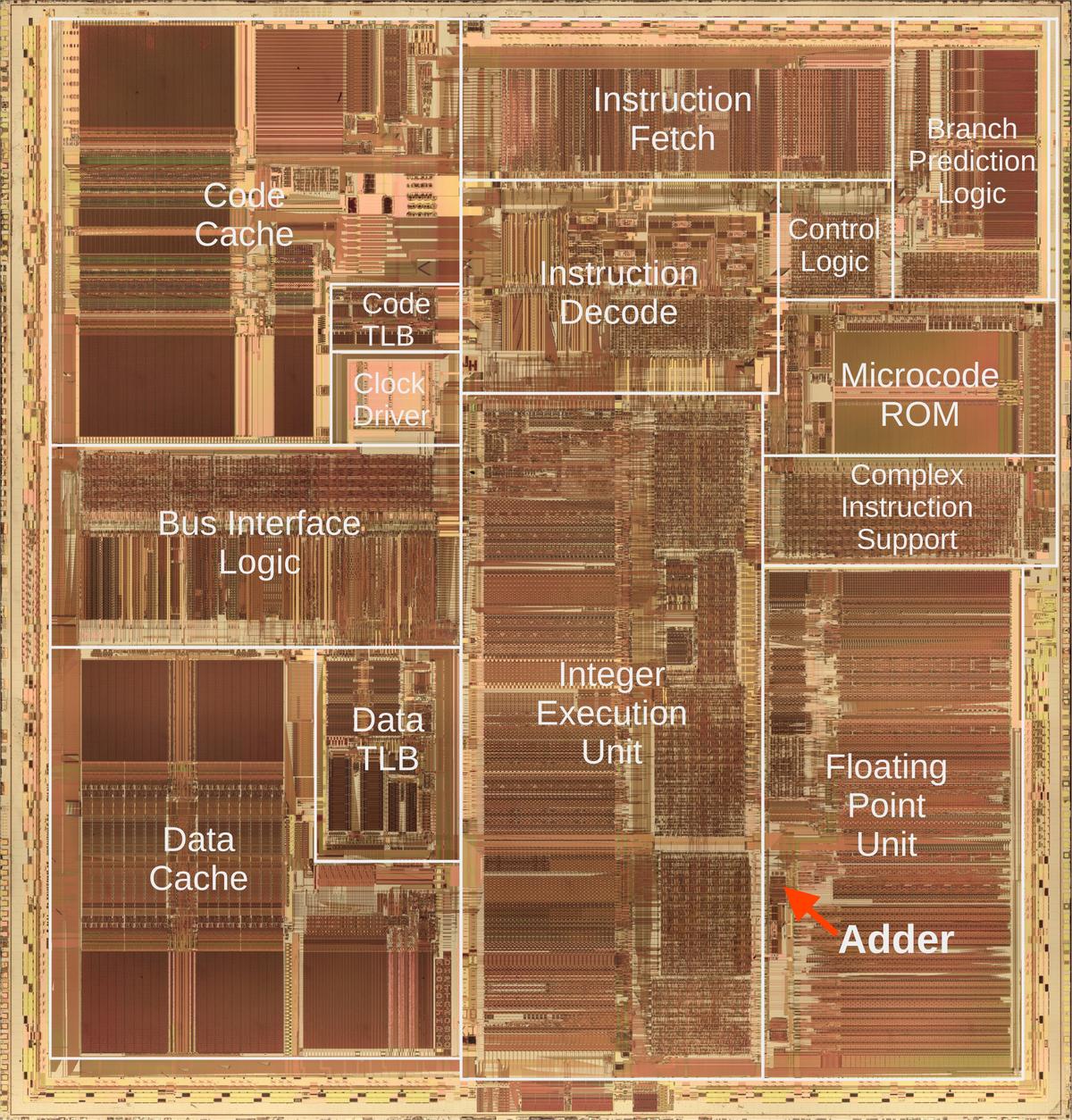
The Pentium die, showing the adder. Click this image (or any other) for a larger version.

The Pentium die, showing the adder. Click this image (or any other) for a larger version.

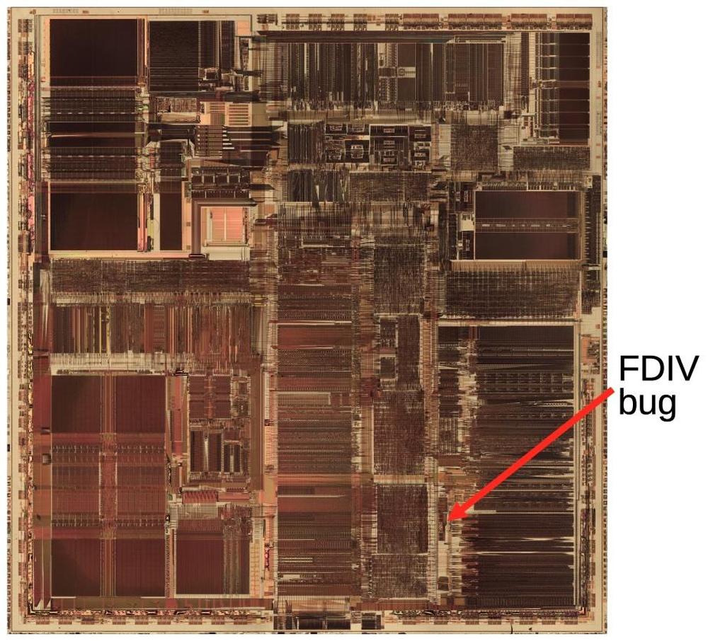
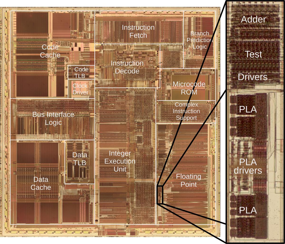
The die photo above shows the main functional units of the Pentium. The adder, in the lower right, is a small component of the floating point unit. It is not a general-purpose adder, but is used only for determining quotient digits during division. It played a role in the famous Pentium FDIV division bug, which I wrote about here.

The hardware implementation

The photo below shows the carry-lookahead adder used by the divider. The adder itself consists of the circuitry highlighted in red. At the top, logic gates compute signals in parallel for each of the 8 pairs of inputs: partial sum, carry generate, and carry propagate. Next, the complex carry-lookahead logic determines in parallel if there will be a carry at each position. Finally, XOR gates apply the carry to each bit. Note that the sum/generate/propagate circuitry consists of 8 repeated blocks, and the same with the carry XOR circuitry. The carry lookahead circuitry, however, doesn't have any visible structure since it is different for each bit.2

The carry-lookahead adder that feeds the lookup table. This block of circuitry is just above the PLA on the die. I removed the metal layers, so this photo shows the doped silicon (dark) and the polysilicon (faint gray).

The carry-lookahead adder that feeds the lookup table. This block of circuitry is just above the PLA on the die. I removed the metal layers, so this photo shows the doped silicon (dark) and the polysilicon (faint gray).

The large amount of circuitry in the middle is used for testing; see the footnote.3 At the bottom, the drivers amplify control signals for various parts of the circuit.

The carry-lookahead adder concept

The problem with addition is that carries make addition slow. Consider calculating 99999+1 by hand. You'll start with 9+1=10, then carry the one, generating another carry, which generates another carry, and so forth, until you go through all the digits. Computer addition has the same problem: If you're adding two numbers, the low-order bits can generate a carry that then propagates through all the bits. An adder that works this way—known as a ripple carry adder—will be slow because the carry has to ripple through all the bits. As a result, CPUs use special circuits to make addition faster.

One solution is the carry-lookahead adder. In this adder, all the carry bits are computed in parallel, before computing the sums. Then, the sum bits can be computed in parallel, using the carry bits. As a result, the addition can be completed quickly, without waiting for the carries to ripple through the entire sum.

It may seem impossible to compute the carries without computing the sum first, but there's a way to do it. For each bit position, you determine signals called "carry generate" and "carry propagate". These signals can then be used to determine all the carries in parallel. The generate signal indicates that the position generates a carry. For instance, if you add binary 1xx and 1xx (where x is an arbitrary bit), a carry will be generated from the top bit, regardless of the unspecified bits. On the other hand, adding 0xx and 0xx will never produce a carry. Thus, the generate signal is produced for the first case but not the second.

But what about 1xx plus 0xx? We might get a carry, for instance, 111+001, but we might not get a carry, for instance, 101+001. In this "maybe" case, we set the carry propagate signal, indicating that a carry into the position will get propagated out of the position. For example, if there is a carry out of the middle position, 1xx+0xx will have a carry from the top bit. But if there is no carry out of the middle position, then there will not be a carry from the top bit. In other words, the propagate signal indicates that a carry into the top bit will be propagated out of the top bit.

To summarize, adding 1+1 will generate a carry. Adding 0+1 or 1+0 will propagate a carry. Thus, the generate signal is formed at each position by Gn = An·Bn, where A and B are the inputs. The propagate signal is Pn = An+Bn, the logical-OR of the inputs.4

Now that the propagate and generate signals are defined, they can be used to compute the carry Cn at each bit position:
C1 = G0: a carry into bit 1 occurs if a carry is generated from bit 0.
C2 = G1 + G0P1: A carry into bit 2 occur if bit 1 generates a carry or bit 1 propagates a carry from bit 0.
C3 = G2 + G1P2 + G0P1P2: A carry into bit 3 occurs if bit 2 generates a carry, or bit 2 propagates a carry generated from bit 1, or bits 2 and 1 propagate a carry generated from bit 0.
C4 = G3 + G2P3 + G1P2P3 + G0P1P2P3: A carry into bit 4 occurs if a carry is generated from bit 3, 2, 1, or 0 along with the necessary propagate signals.
... and so forth, getting more complicated with each bit ...

The important thing about these equations is that they can be computed in parallel, without waiting for a carry to ripple through each position. Once each carry is computed, the sum bits can be computed in parallel: Sn = An ⊕ Bn ⊕ Cn. In other words, the two input bits and the computed carry are combined with exclusive-or.

Implementing carry lookahead with a parallel prefix adder

The straightforward way to implement carry lookahead is to directly implement the equations above. However, this approach requires a lot of circuitry due to the complicated equations. Moreover, it needs gates with many inputs, which are slow for electrical reasons.5

The Pentium's adder implements the carry lookahead in a different way, called the "parallel prefix adder."7 The idea is to produce the propagate and generate signals across ranges of bits, not just single bits as before. For instance, the propagate signal P32 indicates that a carry in to bit 2 would be propagated out of bit 3. And G30 indicates that bits 3 to 0 generate a carry out of bit 3.

Using some mathematical tricks,6 you can take the P and G values for two smaller ranges and merge them into the P and G values for the combined range. For instance, you can start with the P and G values for bits 0 and 1, and produce P10 and G10. These could be merged with P32 and G32 to produce P30 and G30, indicating if a carry is propagated across bits 3-0 or generated by bits 3-0. Note that Gn0 is the carry-lookahead value we need for bit n, so producing these G values gives the results that we need from the carry-lookahead implementation.

This merging process is more efficient than the "brute force" implementation of the carry-lookahead logic since logic subexpressions can be reused. This merging process can be implemented in many ways, including Kogge-Stone, Brent-Kung, and Ladner-Fischer. The different algorithms have different tradeoffs of performance versus circuit area. In the next section, I'll show how the Pentium implements the Kogge-Stone algorithm.

The Pentium's implementation of the carry-lookahead adder

The Pentium's adder is implemented with four layers of circuitry. The first layer produces the propagate and generate signals (P and G) for each bit, along with a partial sum (the sum without any carries). The second layer merges pairs of neighboring P and G values, producing, for instance G65 and P21. The third layer generates the carry-lookahead bits by merging previous P and G values. This layer is complicated because it has different circuitry for each bit. Finally, the fourth layer applies the carry bits to the partial sum, producing the final arithmetic sum.

Here is the schematic of the adder, from my reverse engineering. The circuit in the upper left is repeated 8 times to produce the propagate, generate, and partial sum for each bit. This corresponds to the first layer of logic. At the left are the circuits to merge the generate and propagate signals across pairs of bits. These circuits are the second layer of logic.

Schematic of the Pentium's 8-bit carry-lookahead adder. Click for a larger version.

Schematic of the Pentium's 8-bit carry-lookahead adder. Click for a larger version.

The circuitry at the right is the interesting part—it computes the carries in parallel and then computes the final sum bits using XOR. This corresponds to the third and fourth layers of circuitry respectively. The circuitry gets more complicated going from bottom to top as the bit position increases.

The diagram below is the standard diagram that illustrates how a Kogge-Stone adder works. It's rather abstract, but I'll try to explain it. The diagram shows how the P and G signals are merged to produce each output at the bottom. Each line coresponds to both the P and the G signal. Each square box generates the P and G signals for that bit. (Confusingly, the vertical and diagonal lines have the same meaning, indicating inputs going into a diamond and outputs coming out of a diamond.) Each diamond combines two ranges of P and G signals to generate new P and G signals for the combined range. Thus, the signals cover wider ranges as they progress downward, ending with the Gn0 signals that are the outputs.

A diagram of an 8-bit Kogge-Stone adder highlighting the carry out of bit 6 (green) and out of bit 2 (purple). Modification of the diagram by Robey Pointer, Wikimedia Commons.

A diagram of an 8-bit Kogge-Stone adder highlighting the carry out of bit 6 (green) and out of bit 2 (purple). Modification of the diagram by Robey Pointer, Wikimedia Commons.

It may be easier to understand the diagram by starting with the outputs. I've highlighted two circuits: The purple circuit computes the carry into bit 3 (out of bit 2), while the green circuit computes the carry into bit 7 (out of bit 6). Following the purple output upward, note that it forms a tree reaching bits 2, 1, and 0, so it generates the carry based on these bits, as desired. In more detail, the upper purple diamond combines the P and G signals for bits 2 and 1, generating P21 and G21. The lower purple diamond merges in P0 and G0 to create P20 and G20. Signal G20 indicates of bits 2 through 0 generate a carry; this is the desired carry value into bit 3.

Now, look at the green output and see how it forms a tree going upward, combining bits 6 through 0. Notice how it takes advantage of the purple carry output, reducing the circuitry required. It also uses P65, P43, and the corresponding G signals. Comparing with the earlier schematic shows how the diagram corresponds to the schematic, but abstracts out the details of the gates.

Comparing the diagram to the schematic, each square box corresponds to to the circuit in the upper left of the schematic that generates P and G, the first layer of circuitry. The first row of diamonds corresponds to the pairwise combination circuitry on the left of the schematic, the second layer of circuitry. The remaining diamonds correspond to the circuitry on the right of the schematic, with each column corresponding to a bit, the third layer of circuitry. (The diagram ignores the final XOR step, the fourth layer of circuitry.)

Next, I'll show how the diagram above, the logic equations, and the schematic are related. The diagram below shows the logic equation for C7 and how it is implemented with gates; this corresponds to the green diamonds above. The gates on the left below computes G63; this corresponds to the middle green diamond on the left. The next gate below computes P63 from P65 and P43; this corresponds to the same green diamond. The last gates mix in C3 (the purple line above); this corresponds to the bottom green diamond. As you can see, the diamonds abstract away the complexity of the gates. Finally, the colored boxes below show how the gate inputs map onto the logic equation. Each input corresponds to multiple terms in the equation (6 inputs replace 28 terms), showing how this approach reduces the circuitry required.

This diagram shows how the carry into bit 7 is computed, comparing the equations to the logic circuit.

This diagram shows how the carry into bit 7 is computed, comparing the equations to the logic circuit.

There are alternatives to the Kogge-Stone adder. For example, a Brent-Kung adder (below) uses a different arrangement with fewer diamonds but more layers. Thus, a Brent-Kung adder uses less circuitry but is slower. (You can follow each output upward to verify that the tree reaches the correct inputs.)

A diagram of an 8-bit Brent-Kung adder. Diagram by Robey Pointer, Wikimedia Commons.

A diagram of an 8-bit Brent-Kung adder. Diagram by Robey Pointer, Wikimedia Commons.

Conclusions

The photo below shows the adder circuitry. I've removed the top two layers of metal, leaving the bottom layer of metal. Underneath the metal, polysilicon wiring and doped silicon regions are barely visible; they form the transistors. At the top are eight blocks of gates to generate the partial sum, generate, and propagate signals for each bit. (This corresponds to the first layer of circuitry as described earlier.) In the middle is the carry lookahead circuitry. It is irregular since each bit has different circuitry. (This corresponds to the second and third layers of circuitry, jumbled together.) At the bottom, eight XOR gates combine the carry lookahead output with the partial sum to produce the adder's output. (This corresponds to the fourth layer of circuitry.)

The Pentium's adder circuitry with the top two layers of metal removed.

The Pentium's adder circuitry with the top two layers of metal removed.

The Pentium uses many adders for different purposes: in the integer unit, in the floating point unit, and for address calculation, among others. Floating-point division is known to use a carry-save adder to hold the partial remainder at each step; see my post on the Pentium FDIV division bug for details. I don't know what types of adders are used in other parts of the chip, but maybe I'll reverse-engineer some of them. Follow me on Bluesky (@righto.com) or RSS for updates. (I'm no longer on Twitter.)

Footnotes and references

  1. Strangely, the original paper by Kogge and Stone had nothing to do with addition and carries. Their 1973 paper was titled, "A Parallel Algorithm for the Efficient Solution of a General Class of Recurrence Equations." It described how to solve recurrence problems on parallel computers, in particular the massively parallel ILLIAC IV. As far as I can tell, it wasn't until 1987 that their algorithm was applied to carry lookahead, in Fast Area-Efficient VLSI Adders

  2. I'm a bit puzzled why the circuit uses an 8-bit carry-lookahead adder since only 7 bits are used. Moreover, the carry-out is unused. However, the adder's bottom output bit is not connected to anything. Perhaps the 8-bit adder was a standard logic block at Intel and was used as-is. 

  3. I probably won't make a separate blog post on the testing circuitry, so I'll put details in this footnote. Half of the circuitry in the adder block is used to test the lookup table. The reason is that a chip such as the Pentium is very difficult to test: if one out of 3.1 million transistors goes bad, how do you detect it? For a simple processor like the 8080, you can run through the instruction set and be fairly confident that any problem would turn up. But with a complex chip, it is almost impossible to come up with an instruction sequence that would test every bit of the microcode ROM, every bit of the cache, and so forth. Starting with the 386, Intel added circuitry to the processor solely to make testing easier; about 2.7% of the transistors in the 386 were for testing.

    To test a ROM inside the processor, Intel added circuitry to scan the entire ROM and checksum its contents. Specifically, a pseudo-random number generator runs through each address, while another circuit computes a checksum of the ROM output, forming a "signature" word. At the end, if the signature word has the right value, the ROM is almost certainly correct. But if there is even a single bit error, the checksum will be wrong and the chip will be rejected. The pseudo-random numbers and the checksum are both implemented with linear feedback shift registers (LFSR), a shift register along with a few XOR gates to feed the output back to the input. For more information on testing circuitry in the 386, see Design and Test of the 80386, written by Pat Gelsinger, who became Intel's CEO years later. Even with the test circuitry, 48% of the transistor sites in the 386 were untested. The instruction-level test suite to test the remaining circuitry took almost 800,000 clock cycles to run. The overhead of the test circuitry was about 10% more transistors in the blocks that were tested.

    In the Pentium, the circuitry to test the lookup table PLA is just below the 7-bit adder. An 11-bit LFSR creates the 11-bit input value to the lookup table. A 13-bit LFSR hashes the two-bit quotient result from the PLA, forming a 13-bit checksum. The checksum is fed serially to test circuitry elsewhere in the chip, where it is merged with other test data and written to a register. If the register is 0 at the end, all the tests pass. In particular, if the checksum is correct, you can be 99.99% sure that the lookup table is operating as expected. The ironic thing is that this test circuit was useless for the FDIV bug: it ensured that the lookup table held the intended values, but the intended values were wrong.

    Why did Intel generate test addresses with a pseudo-random sequence instead of a sequential counter? It turns out that a linear feedback shift register (LFSR) is slightly more compact than a counter. This LFSR trick was also used in a touch-tone chip and the program counter of the Texas Instruments TMS 1000 microcontroller (1974). In the TMS 1000, the program counter steps through the program pseudo-randomly rather than sequentially. The program is shuffled appropriately in the ROM to counteract the sequence, so the program executes as expected and a few transistors are saved.

    Block diagram of the testing circuitry.

    Block diagram of the testing circuitry.
  4. The bits 1+1 will set generate, but should propagate be set too? It doesn't make a difference as far as the equations. This adder sets propagate for 1+1 but some other adders do not. The answer depends on if you use an inclusive-or or exclusive-or gate to produce the propagate signal. 

  5. One solution is to implement the carry-lookahead circuit in blocks of four. This can be scaled up with a second level of carry-lookahead to provide the carry lookahead across each group of four blocks. A third level can provide carry lookahead for groups of four second-level blocks, and so forth. This approach requires O(log(N)) levels for N-bit addition. This approach is used by the venerable 74181 ALU, a chip used by many minicomputers in the 1970s; I reverse-engineered the 74181 here. The 74182 chip provides carry lookahead for the higher levels. 

  6. I won't go into the mathematics of merging P and G signals; see, for example, Adder Circuits, Adders, or Carry Lookahead Adders for additional details. The important factor is that the carry merge operator is associative (actually a monoid), so the sub-ranges can be merged in any order. This flexibility is what allows different algorithms with different tradeoffs. 

  7. The idea behind a prefix adder is that we want to see if there is a carry out of bit 0, bits 0-1, bits 0-2, bits 0-3, 0-4, and so forth. These are all the prefixes of the word. Since the prefixes are computed in parallel, it's called a parallel prefix adder. 

The origin of the cargo cult metaphor

The cargo cult metaphor is commonly used by programmers. This metaphor was popularized by Richard Feynman's "cargo cult science" talk with a vivid description of South Seas cargo cults. However, this metaphor has three major problems. First, the pop-culture depiction of cargo cults is inaccurate and fictionalized, as I'll show. Second, the metaphor is overused and has contradictory meanings making it a lazy insult. Finally, cargo cults are portrayed as an amusing story of native misunderstanding but the background is much darker: cargo cults are a reaction to decades of oppression of Melanesian islanders and the destruction of their culture. For these reasons, the cargo cult metaphor is best avoided.

Members of the John Frum cargo cult, marching with bamboo "rifles". Photo adapted from The Open Encyclopedia of Anthropology, (CC BY-NC 4.0).

Members of the John Frum cargo cult, marching with bamboo "rifles". Photo adapted from The Open Encyclopedia of Anthropology, (CC BY-NC 4.0).

In this post, I'll describe some cargo cults from 1919 to the present. These cargo cults are completely different from the description of cargo cults you usually find on the internet, which I'll call the "pop-culture cargo cult." Cargo cults are extremely diverse, to the extent that anthropologists disagree on the cause, definition, or even if the term has value. I'll show that many of the popular views of cargo cults come from a 1962 "shockumentary" called Mondo Cane. Moreover, most online photos of cargo cults are fake.

Feynman and Cargo Cult Science

The cargo cult metaphor in science started with Professor Richard Feynman's well-known 1974 commencement address at Caltech.1 This speech, titled "Cargo Cult Science", was expanded into a chapter in his best-selling 1985 book "Surely You're Joking, Mr. Feynman". He said:

In the South Seas there is a cargo cult of people. During the war they saw airplanes land with lots of good materials, and they want the same thing to happen now. So they’ve arranged to make things like runways, to put fires along the sides of the runways, to make a wooden hut for a man to sit in, with two wooden pieces on his head like headphones and bars of bamboo sticking out like antennas—he’s the controller—and they wait for the airplanes to land. They’re doing everything right. The form is perfect. It looks exactly the way it looked before. But it doesn’t work. No airplanes land. So I call these things cargo cult science, because they follow all the apparent precepts and forms of scientific investigation, but they’re missing something essential, because the planes don’t land.

Richard Feynman giving the 1974 commencement address at Caltech. Photo from Wikimedia Commons.

Richard Feynman giving the 1974 commencement address at Caltech. Photo from Wikimedia Commons.

But the standard anthropological definition of "cargo cult" is entirely different: 2

Cargo cults are strange religious movements in the South Pacific that appeared during the last few decades. In these movements, a prophet announces the imminence of the end of the world in a cataclysm which will destroy everything. Then the ancestors will return, or God, or some other liberating power, will appear, bringing all the goods the people desire, and ushering in a reign of eternal bliss.

An anthropology encyclopedia gives a similar definition:

A southwest Pacific example of messianic or millenarian movements once common throughout the colonial world, the modal cargo cult was an agitation or organised social movement of Melanesian villagers in pursuit of ‘cargo’ by means of renewed or invented ritual action that they hoped would induce ancestral spirits or other powerful beings to provide. Typically, an inspired prophet with messages from those spirits persuaded a community that social harmony and engagement in improvised ritual (dancing, marching, flag-raising) or revived cultural traditions would, for believers, bring them cargo.
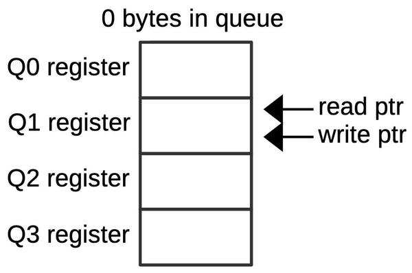
As you may see, the pop-culture explanation of a cargo cult and the anthropological definition are completely different, apart from the presence of "cargo" of some sort. Have anthropologists buried cargo cults under layers of theory? Are they even discussing the same thing? My conclusion, after researching many primary sources, is that the anthropological description accurately describes the wide variety of cargo cults. The pop-culture cargo cult description, however, takes features of some cargo cults (the occasional runway) and combines this with movie scenes to yield an inaccurate and fictionalized dscription. It may be hard to believe that the description of cargo cults that you see on the internet is mostly wrong, but in the remainder of this article, I will explain this in detail.
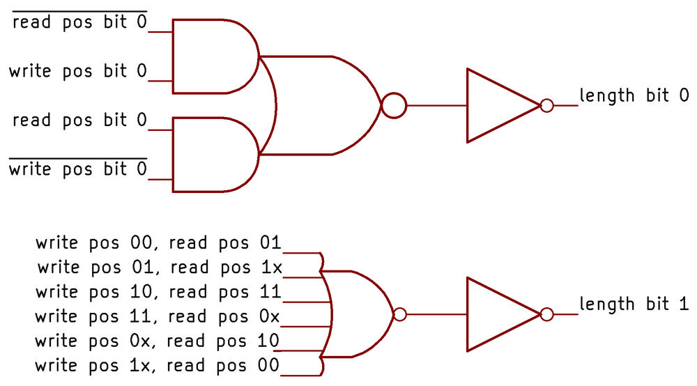
Background on Melanesia

Cargo cults occur in a specific region of the South Pacific called Melanesia. I'll give a brief (oversimplified) description of Melanesia to provide important background. The Pacific Ocean islands are divided into three cultural areas: Polynesia, Micronesia, and Melanesia. Polynesia is the best known, including Hawaii, New Zealand, and Samoa. Micronesia, in the northwest, consists of thousands of small islands, of which Guam is the largest; the name "Micronesia" is Greek for "small island". Melanesia, the relevant area for this article, is a group of islands between Micronesia and Australia, including Fiji, Vanuatu, Solomon Islands, and New Guinea. (New Guinea is the world's second-largest island; confusingly, the country of Papua New Guinea occupies the eastern half of the island, while the western half is part of Indonesia.)

Major cultural areas of Oceania. Image by https://commons.wikimedia.org/wiki/File:Pacific_Culture_Areas.jpg.

The inhabitants of Melanesia typically lived in small villages of under 200 people, isolated by mountainous geography. They had a simple, subsistence economy, living off cultivated root vegetables, pigs, and hunting. People tended their own garden, without specialization into particular tasks. The people of Melanesia are dark-skinned, which will be important ("Melanesia" and "melanin" have the same root). Technologically, the Melanesians used stone, wood, and shell tools, without knowledge of metallurgy or even weaving. The Melanesian cultures were generally violent3 with everpresent tribal warfare and cannibalism.4

Due to the geographic separation of tribes, New Guinea became the most linguistically diverse country in the world, with over 800 distinct languages. Pidgin English was often the only way for tribes to communicate, and is now one of the official languages of New Guinea. This language, called Tok Pisin (i.e. "talk pidgin"), is now the most common language in Papua New Guinea, spoken by over two-thirds of the population.5

For the Melanesians, religion was a matter of ritual, rather than a moral framework. It is said that "to the Melanesian, a religion is above all a technology: it is the knowledge of how to bring the community into the correct relation, by rites and spells, with the divinities and spirit-beings and cosmic forces that can make or mar man's this-worldly wealth and well-being." This is important since, as will be seen, the Melanesians expected that the correct ritual would result in the arrival of cargo. Catholic and Protestant missionaries converted the inhabitants to Christianity, largely wiping out traditional religious practices and customs; Melanesia is now over 95% Christian. Christianity played a large role in cargo cults, as will be shown below.

European explorers first reached Melanesia in the 1500s, followed by colonization.6 By the end of the 1800s, control of the island of New Guinea was divided among Germany, Britain, and the Netherlands. Britain passed responsibility to Australia in 1906 and Australia gained the German part of New Guinea in World War I. As for the islands of Vanuatu, the British and French colonized them (under the name New Hebrides) in the 18th century.

The influx of Europeans was highly harmful to the Melanesians. "Native society was severely disrupted by war, by catastrophic epidemics of European diseases, by the introduction of alcohol, by the devastation of generations of warfare, and by the depredations of the labour recruiters."8 People were kidnapped and forced to work as laborers in other countries, a practice called blackbirding. Prime agricultural land was taken by planters to raise crops such as coconuts for export, with natives coerced into working for the planters.9 Up until 1919, employers were free to flog the natives for disobedience; afterward, flogging was technically forbidden but still took place. Colonial administrators jailed natives who stepped out of line.7

Cargo cults before World War II

While the pop-culture cargo cults explains them as a reaction to World War II, cargo cults started years earlier. One anthropologist stated, "Cargo cults long preceded [World War II], continued to occur during the war, and have continued to the present."

The first writings about cargo cult behavior date back to 1919, when it was called the "Vailala Madness":10

The natives were saying that the spirits of their ancestors had appeared to several in the villages and told them that all flour, rice, tobacco, and other trade belonged to the New Guinea people, and that the white man had no right whatever to these goods; in a short time all the white men were to be driven away, and then everything would be in the hands of the natives; a large ship was also shortly to appear bringing back the spirits of their departed relatives with quantities of cargo, and all the villages were to make ready to receive them.

The 1926 book In Unknown New Guinea also describes the Vialala Madness:11

[The leader proclaimed] that the ancestors were coming back in the persons of the white people in the country and that all the things introduced by the white people and the ships that brought them belonged really to their ancestors and themselves. [He claimed that] he himself was King George and his friend was the Governor. Christ had given him this authority and he was in communication with Christ through a hole near his village.

The Melanesians blamed the Europeans for the failure of cargo to arrive. In the 1930s, one story was that because the natives had converted to Christianity, God was sending the ancestors with cargo that was loaded on ships. However, the Europeans were going through the cargo holds and replacing the names on the crates so the cargo was fraudulently delivered to the Europeans instead of the rightful natives.

The Mambu Movement occurred in 1937. Mambu, the movement's prophet, claimed that "the Whites had deceived the natives. The ancestors lived inside a volcano on Manum Island, where they worked hard making goods for their descendants: loin-cloths, socks, metal axes, bush-knives, flashlights, mirrors, red dye, etc., even plank-houses, but the scoundrelly Whites took the cargoes. Now this was to stop. The ancestors themselves would bring the goods in a large ship." To stop this movement, the Government arrested Mambu, exiled him, and imprisoned him for six months in 1938.

To summarize, these early cargo cults believed that ships would bring cargo that rightfully belonged to the natives but had been stolen by the whites. The return of the cargo would be accompanied by the spirits of the ancestors. Moreover, Christianity often played a large role. A significant racial component was present, with natives driving out the whites or becoming white themselves.

Cargo cults in World War II and beyond

World War II caused tremendous social and economic upheavals in Melanesia. Much of Melanesia was occupied by Japan near the beginning of the war and the Japanese treated the inhabitants harshly. The American entry into the war led to heavy conflict in the area such as the arduous New Guinea campaign (1942-1945) and the Solomon Islands campaign. As the Americans and Japanese battled for control of the islands, the inhabitants were caught in the middle. Papua and New Guinea suffered over 15,000 civilian deaths, a shockingly high number for such a small region.12


The photo shows a long line of F4F Wildcats at Henderson Field, Guadalcanal, Solomon Islands, April 14, 1943.
Solomon Islands was home to several cargo cults, both before and after World War II (see map).
Source: US Navy photo 80-G-41099.

The photo shows a long line of F4F Wildcats at Henderson Field, Guadalcanal, Solomon Islands, April 14, 1943. Solomon Islands was home to several cargo cults, both before and after World War II (see map). Source: US Navy photo 80-G-41099.

The impact of the Japanese occupation on cargo cults is usually ignored. One example from 1942 is a cargo belief that the Japanese soldiers were spirits of the dead, who were being sent by Jesus to liberate the people from European rule. The Japanese would bring the cargo by airplane since the Europeans were blocking the delivery of cargo by ship. This would be accompanied by storms and earthquakes, and the natives' skin would change from black to white. The natives were to build storehouses for the cargo and fill the storehouses with food for the ancestors. The leader of this movement, named Tagarab, explained that he had an iron rod that gave him messages about the future. Eventually, the Japanese shot Tagarab, bringing an end to this cargo cult.13

The largest and most enduring cargo cult is the John Frum movement, which started on the island of Tanna around 1941 and continues to the present. According to one story, a mythical person known as John Frum, master of the airplanes, would reveal himself and drive off the whites. He would provide houses, clothes, and food for the people of Tanna. The island of Tanna would flatten as the mountains filled up the valleys and everyone would have perfect health. In other areas, the followers of John Frum believed they "would receive a great quantity of goods, brought by a white steamer which would come from America." Families abandoned the Christian villages and moved to primitive shelters in the interior. They wildly spent much of their money and threw the rest into the sea. The government arrested and deported the leaders, but that failed to stop the movement. The identity of John Frum is unclear; he is sometimes said to be a white American while in other cases natives have claimed to be John Frum.14

The cargo cult of Kainantu17 arose around 1945 when a "spirit wind" caused people in the area to shiver and shake. Villages built large "cargo houses" and put stones, wood, and insect-marked leaves inside, representing European goods, rifles, and paper letters respectively. They killed pigs and anointed the objects, the house, and themselves with blood. The cargo house was to receive the visiting European spirit of the dead who would fill the house with goods. This cargo cult continued for about 5 years, diminishing as people became disillusioned by the failure of the goods to arrive.

The name "Cargo Cult" was first used in print in 1945, just after the end of World War II.15 The article blamed the problems on the teachings of missionaries, with the problems "accentuated a hundredfold" by World War II.

Stemming directly from religious teaching of equality, and its resulting sense of injustice, is what is generally known as “Vailala Madness,” or “Cargo Cult.” "In all cases the "Madness" takes the same form: A native, infected with the disorder, states that he has been visited by a relative long dead, who stated that a great number of ships loaded with "cargo" had been sent by the ancestor of the native for the benefit of the natives of a particular village or area. But the white man, being very cunning, knows how to intercept these ships and takes the "cargo" for his own use... Livestock has been destroyed, and gardens neglected in the expectation of the magic cargo arriving. The natives infected by the "Madness" sank into indolence and apathy regarding common hygiene."

In a 1946 episode, agents of the Australian government found a group of New Guinea highlanders who believed that the arrival of the whites signaled that the end of the world was at hand. The highlanders butchered all their pigs in the expectation that "Great Pigs" would appear from the sky in three days. At this time, the residents would exchange their black skin for white skin. They created mock radio antennas of bamboo and rope to receive news of the millennium.16

The New York Times described Cargo Cults in 1948 as "the belief that a convoy of cargo ships is on its way, laden with the fruits of the modern world, to outfit the leaf huts of the natives." The occupants of the British Solomon Islands were building warehouses along the beaches to hold these goods. Natives marched into a US Army camp, presented $3000 in US money, and asked the Army to drive out the British.

A 1951 paper described cargo cults: "The insistence that a 'cargo' of European goods is to be sent by the ancestors or deceased spirits; this may or may not be part of a general reaction against Europeans, with an overtly expressed desire to be free from alien domination. Usually the underlying theme is a belief that all trade goods were sent by ancestors or spirits as gifts for their descendants, but have been misappropriated on the way by Europeans."17

In 1959, The New York Times wrote about cargo cults: "Rare Disease and Strange Cult Disturb New Guinea Territory; Fatal Laughing Sickness Is Under Study by Medical Experts—Prophets Stir Delusions of Food Arrivals". The article states that "large native groups had been infected with the idea that they could expect the arrival of spirit ships carrying large supplies of food. In false anticipation of the arrival of the 'cargoes', 5000 to 7000 native have been known to consume their entire food reserve and create a famine." As for "laughing sickness", this is now known to be a prion disease transmitted by eating human brains. In some communities, this disease, also called Kuru, caused 50% of all deaths.

A detailed 1959 article in Scientific American, "Cargo Cults", described many different cargo cults.16 It lists various features of cargo cults, such as the return of the dead, skin color switching from black to white, threats against white rule, and belief in a coming messiah. The article finds a central theme in cargo cults: "The world is about to end in a terrible cataclysm. Thereafter God, the ancestors or some local culture hero will appear and inaugurate a blissful paradise on earth. Death, old age, illness and evil will be unknown. The riches of the white man will accrue to the Melanesians."

In 1960, the celebrated naturalist David Attenborough created a documentary The People of Paradise: Cargo Cult.18 Attenborough travels through the island of Tanna and encounters many artifacts of the John Frum cult, such as symbolic gates and crosses, painted brilliant scarlet and decorated with objects such as a shaving brush, a winged rat, and a small carved airplane. Attenborough interviews a cult leader who claims to have talked with the mythical John Frum, said to be a white American. The leader remains in communication with John Frum through a tall pole said to be a radio mast, and an unseen radio. (The "radio" consisted of an old woman with electrical wire wrapper around her waist, who would speak gibberish in a trance.)

"Symbols of the cargo cult." In the center, a representation of John Frum with "scarlet coat and a white European face" stands behind a brilliantly painted cross. A wooden airplane is on the right, while on the left (outside the photo) a cage contains a winged rat. From Journeys to the Past, which describes Attenborough's visit to the island of Tanna.

"Symbols of the cargo cult." In the center, a representation of John Frum with "scarlet coat and a white European face" stands behind a brilliantly painted cross. A wooden airplane is on the right, while on the left (outside the photo) a cage contains a winged rat. From Journeys to the Past, which describes Attenborough's visit to the island of Tanna.

In 1963, famed anthropologist Margaret Mead brought cargo cults to the general public, writing Where Americans are Gods: The Strange Story of the Cargo Cults in the mass-market newspaper supplement Family Weekly. In just over a page, this article describes the history of cargo cults before, during, and after World War II.19 One cult sat around a table with vases of colorful flowers on them. Another cult threw away their money. Another cult watched for ships from hilltops, expecting John Frum to bring a fleet of ships bearing cargo from the land of the dead.

One of the strangest cargo cults was a group of 2000 people on New Hanover Island, "collecting money to buy President Johnson of the United States [who] would arrive with other Americans on the liner Queen Mary and helicopters next Tuesday." The islanders raised $2000, expecting American cargo to follow the president. Seeing the name Johnson on outboard motors confirmed their belief that President Johnson was personally sending cargo.20

A 1971 article in Time Magazine22 described how tribesmen brought US Army concrete survey markers down from a mountaintop while reciting the Roman Catholic rosary, dropping the heavy markers outside the Australian government office. They expected that "a fleet of 500 jet transports would disgorge thousands of sympathetic Americans bearing crates of knives, steel axes, rifles, mirrors and other wonders." Time magazine explained the “cargo cult” as "a conviction that if only the dark-skinned people can hit on the magic formula, they can, without working, acquire all the wealth and possessions that seem concentrated in the white world... They believe that everything has a deity who has to be contacted through ritual and who only then will deliver the cargo." Cult leaders tried "to duplicate the white man’s magic. They hacked airstrips in the rain forest, but no planes came. They built structures that look like white men’s banks, but no money materialized."21

National Geographic, in an article Head-hunters in Today's World (1972), mentioned a cargo-cult landing field with a replica of a radio aerial, created by villagers who hoped that it would attract airplanes bearing gifts. It also described a cult leader in South Papua who claimed to obtain airplanes and cans of food from a hole in the ground. If the people believed in him, their skins would turn white and he would lead them to freedom.

These sources and many others23 illustrate that cargo cults do not fit a simple story. Instead, cargo cults are extremely varied, happening across thousands of miles and many decades. The lack of common features between cargo cults leads some anthropologists to reject the idea of cargo cults as a meaningful term.24 In any case, most historical cargo cults have very little in common with the pop-culture description of a cargo cult.

Cargo beliefs were inspired by Christianity

Cargo cult beliefs are closely tied to Christianity, a factor that is ignored in pop-culture descriptions of cargo cults. Beginning in the mid-1800s, Christian missionaries set up churches in New Guinea to convert the inhabitants. As a result, cargo cults incorporated Christian ideas, but in very confusing ways. At first, the natives believed that missionaries had come to reveal the ritual secrets and restore the cargo. By enthusiastically joining the church, singing the hymns, and following the church's rituals, the people would be blessed by God, who would give them the cargo. This belief was common in the 1920s and 1930s, but as the years went on and the people didn't receive the cargo, they theorized that the missionaries had removed the first pages of the Bible to hide the cargo secrets.

A typical belief was that God created Adam and Eve in Paradise, "giving them cargo: tinned meat, steel tools, rice in bags, tobacco in tins, and matches, but not cotton clothing." When Adam and Eve offended God by having sexual intercourse, God threw them out of Paradise and took their cargo. Eventually, God sent the Flood but Noah was saved in a steamship and God gave back the cargo. Noah's son Ham offended God, so God took the cargo away from Ham and sent him to New Guinea, where he became the ancestor of the natives.

Other natives believed that God lived in Heaven, which was in the clouds and reachable by ladder from Sydney, Australia (source). God, along with the ancestors, created cargo in Heaven—"tinned meat, bags of rice, steel tools, cotton cloth, tinned tobacco, and a machine for making electric light"—which would be flown from Sydney and delivered to the natives, who thus needed to clear an airstrip (source).25

Another common belief was that symbolic radios could be used to communicate with Jesus. For instance, a Markham Valley cargo group in 1943 created large radio houses so they could be informed of the imminent Coming of Jesus, at which point the natives would expel the whites (source). The "radio" consisted of bamboo cylinders connected to a rope "aerial" strung between two poles. The houses contained a pole with rungs so the natives could climb to Jesus along with cane "flashlights" to see Jesus.

A tall mast with a flag and cross on top. This was claimed to be a special radio mast that enabled
communication with John Frum. It was decorated with scarlet leaves and flowers.
From Attenborough's Cargo Cult.

A tall mast with a flag and cross on top. This was claimed to be a special radio mast that enabled communication with John Frum. It was decorated with scarlet leaves and flowers. From Attenborough's Cargo Cult.

Mock radio antennas are also discussed in a 1943 report26 from a wartime patrol that found a bamboo "wireless house", 42 feet in diameter. It had two long poles outside and with an "aerial" of rope between them, connected to the "radio" inside, a bamboo cylinder. Villagers explained that the "radio" was to receive messages of the return of Jesus, who would provide weapons for the overthrow of white rule. The villagers constructed ladders outside the house so they could climb up to the Christian God after death. They would shed their skin like a snake, getting a new white skin, and then they would receive the "boats and white men's clothing, goods, etc."

Mondo Cane and the creation of the pop-culture cargo cult

As described above, cargo cults expected the cargo to arrive by ships much more often than airplanes. So why do pop-culture cargo cults have detailed descriptions of runways, airplanes, wooden headphones, and bamboo control towers?27 My hypothesis is that it came from a 1962 movie called Mondo Cane. This film was the first "shockumentary", showing extreme and shocking scenes from around the world. Although the film was highly controversial, it was shown at the Cannes Film Festival and was a box-office success.

The film made extensive use of New Guinea with multiple scandalous segments, such as a group of "love-struck" topless women chasing men,29 a woman breastfeeding a pig, and women in cages being fattened for marriage. The last segment in the movie showed "the cult of the cargo plane": natives forlornly watching planes at the airport, followed by scenes of a bamboo airplane sitting on a mountaintop "runway" along with bamboo control towers. The natives waited all day and then lit torches to illuminate the runway at nightfall. These scenes are very similar to the pop-culture descriptions of cargo cults so I suspect this movie is the source.

A still from the 1962 movie "Mondo Cane", showing a bamboo airplane sitting on a runway, with flaming torches acting as beacons. I have my doubts about its accuracy.

A still from the 1962 movie "Mondo Cane", showing a bamboo airplane sitting on a runway, with flaming torches acting as beacons. I have my doubts about its accuracy.

The film claims that all the scenes "are true and taken only from life", but many of the scenes are said to be staged. Since the cargo cult scenes are very different from anthropological reports and much more dramatic, I think they were also staged and exaggerated.28 It is known that the makers of Mondo Cane paid the Melanesian natives generously for the filming (source, source).

Did Feynman get his cargo cult ideas from Mondo Cane? It may seem implausible since the movie was released over a decade earlier. However, the movie became a cult classic, was periodically shown in theaters, and influenced academics.30 In particular, Mondo Cane showed at the famed Cameo theater in downtown Los Angeles on April 3, 1974, two months before Feynman's commencement speech. Mondo Cane seems like the type of offbeat movie that Feynman would see and the theater was just 11 miles from Caltech. While I can't prove that Feynman went to the showing, his description of a cargo cult strongly resembles the movie.31

Fake cargo-cult photos fill the internet

Fakes and hoaxes make researching cargo cults online difficult. There are numerous photos online of cargo cults, but many of these photos are completely made up. For instance, the photo below has illustrated cargo cults for articles such as Cargo Cult, UX personas are useless, A word on cargo cults, The UK Integrated Review and security sector innovation, and Don't be a cargo cult. However, this photo is from a Japanese straw festival and has nothing to do with cargo cults.

An airplane built from straw, one creation at a Japanese straw festival. I've labeled the photo with "Not cargo cult" to ensure it doesn't get reused in cargo cult articles.

An airplane built from straw, one creation at a Japanese straw festival. I've labeled the photo with "Not cargo cult" to ensure it doesn't get reused in cargo cult articles.

Another example is the photo below, supposedly an antenna created by a cargo cult. However, it is actually a replica of the Jodrell Bank radio telescope, built in 2007 by a British farmer from six tons of straw (details). The farmer's replica ended up erroneously illustrating Cargo Cult Politics, The Cargo Cult & Beliefs, The Cargo Cult, Cargo Cults of the South Pacific, and Cargo Cult, among others.32

A British farmer created this replica radio telescope. Photo by Mike Peel, (CC BY-SA 4.0).

A British farmer created this replica radio telescope. Photo by Mike Peel, (CC BY-SA 4.0).

Other articles illustrate cargo cults with the aircraft below, suspiciously sleek and well-constructed. However, the photo actually shows a wooden wind tunnel model of the Buran spacecraft, abandoned at a Russian airfield as described in this article. Some uses of the photo are Are you guilty of “cargo cult” thinking without even knowing it? and The Cargo Cult of Wealth.

This is an abandoned Soviet wind tunnel model of the Buran spacecraft. Photo by Aleksandr Markin.

This is an abandoned Soviet wind tunnel model of the Buran spacecraft. Photo by Aleksandr Markin.

Many cargo cult articles use one of the photo below. I tracked them down to the 1970 movie "Chariots of the Gods" (link), a dubious documentary claiming that aliens have visited Earth throughout history. The segment on cargo cults is similar to Mondo Cane with cultists surrounding a mock plane on a mountaintop, lighting fires along the runway. However, it is clearly faked, probably in Africa: the people don't look like Pacific Islanders and are wearing wigs. One participant wears leopard skin (leopards don't live in the South Pacific). The vegetation is another giveaway: the plants are from Africa, not the South Pacific.33

Two photos of a straw plane from "Chariots of the Gods".

Two photos of a straw plane from "Chariots of the Gods".

The point is that most of the images that illustrate cargo cults online are fake or wrong. Most internet photos and information about cargo cults have just been copied from page to page. (And now we have AI-generated cargo cult photos.) If a photo doesn't have a clear source (including who, when, and where), don't believe it.

Conclusions

The cargo cult metaphor should be avoided for three reasons. First, the metaphor is essentially meaningless and heavily overused. The influential "Jargon File" defined cargo-cult programming as "A style of (incompetent) programming dominated by ritual inclusion of code or program structures that serve no real purpose."34 Note that the metaphor in cargo-cult programming is the opposite of the metaphor in cargo-cult science: Feyman's cargo-cult science has no chance of working, while cargo-cult programming works but isn't understood. Moreover, both metaphors differ from the cargo-cult metaphor in other contexts, referring to the expectation of receiving valuables without working.35

The popular site Hacker News is an example of how "cargo cult" can be applied to anything: agile programming, artificial intelligence, cleaning your desk. Go, hatred of Perl, key rotation, layoffs, MBA programs, microservices, new drugs, quantum computing, static linking, test-driven development, and updating the copyright year are just a few things that are called "cargo cult".36 At this point, cargo cult is simply a lazy, meaningless attack.

The second problem with "cargo cult" is that the pop-culture description of cargo cults is historically inaccurate. Actual cargo cults are much more complex and include a much wider (and stranger) variety of behaviors. Cargo cults started before World War II and involve ships more often than airplanes. Cargo cults mix aspects of paganism and Christianity, often with apocalyptic ideas of the end of the current era, the overthrow of white rule, and the return of dead ancestors. The pop-culture description discards all this complexity, replacing it with a myth.

Finally, the cargo cult metaphor turns decades of harmful colonialism into a humorous anecdote. Feynman's description of cargo cults strips out the moral complexity: US soldiers show up with their cargo and planes, the indigenous residents amusingly misunderstand the situation, and everyone carries on. However, cargo cults really were a response to decades of colonial mistreatment, exploitation, and cultural destruction. Moreover, cargo cults were often harmful: expecting a bounty of cargo, villagers would throw away their money, kill their pigs, and stop tending their crops, resulting in famine. The pop-culture cargo cult erases the decades of colonial oppression, along with the cultural upheaval and deaths from World War II. Melanesians deserve to be more than the punch line in a cargo cult story.

Thus, it's time to move beyond the cargo cult metaphor.

Update: well, this sparked much more discussion on Hacker News than I expected. To answer some questions: Am I better or more virtuous than other people? No. Are you a bad person if you use the cargo cult metaphor? No. Is "cargo cult" one of many Hacker News comments that I'm tired of seeing? Yes (details). Am I criticizing Feynman? No. Do the Melanesians care about this? Probably not. Did I put way too much research into this? Yes. Is criticizing colonialism in the early 20th century woke? I have no response to that.

Notes and references

  1. As an illustration of the popularity of Feynman's "Cargo Cult Science" commencement address, it has been on Hacker News at least 15 times. 

  2. The first cargo cult definition above comes from The Trumpet Shall Sound; A Study of "Cargo" Cults in Melanesia. The second definition is from the Cargo Cult entry in The Open Encyclopedia of Anthropology. Written by Lamont Lindstrom, a professor who studies Melanesia, the entry comprehensively describes the history and variety of cargo cults, as well as current anthropological analysis.

    For an early anthropological theory of cargo cults, see An Empirical Case-Study: The Problem of Cargo Cults in "The Revolution in Anthropology" (Jarvie, 1964). This book categorizes cargo cults as an apocalyptic millenarian religious movement with a central tenet:

    When the millennium comes it will largely consist of the arrival of ships and/or aeroplanes loaded up with cargo; a cargo consisting either of material goods the natives long for (and which are delivered to the whites in this manner), or of the ancestors, or of both.
     
  3. European colonization brought pacification and a reduction in violence. The Cargo Cult: A Melanesian Type-Response to Change describes this pacification and termination of warfare as the Pax Imperii, suggesting that pacification came as a relief to the Melanesians: "They welcomed the cessation of many of the concomitants of warfare: the sneak attack, ambush, raiding, kidnapping of women and children, cannibalism, torture, extreme indignities inflicted on captives, and the continual need to be concerned with defense." That article calls the peace the Pax Imperii.

    Warfare among the Enga people of New Guinea is described in From Spears to M-16s: Testing the Imbalance of Power Hypothesis among the Enga. The Enga engaged in tribal warfare for reasons such as "theft of game from traps, quarrels over possessions, or work sharing within the group." The surviving losers were usually driven off the land and forced to settle elsewhere. In the 1930s and 1940s, the Australian administration banned tribal fighting and pacified much of the area. However, after the independence of Papua New Guinea in 1975, warfare increased along with the creation of criminal gangs known as Raskols (rascals). The situation worsened in the late 1980s with the introduction of shotguns and high-powered weapons to warfare. Now, Papua New Guinea has one of the highest crime rates in the world along with one of the lowest police-to-population ratios in the world. 

  4. When you hear tales of cannibalism, some skepticism is warranted. However, cannibalism is proved by the prevalence of kuru, or "laughing sickness", a fatal prion disease (transmissible spongiform encephalopathy) spread by consuming human brains. Also see Headhunters in Today's World, a 1972 National Geographic article that describes the baking of heads and the eating of brains. 

  5. A 1957 dictionary of Pidgin English can be found here. Linguistically, Tok Pisin is a creole, not a pidgin. 

  6. The modern view is that countries such as Great Britain acquired colonies against the will of the colonized, but the situation was more complex in the 19th century. Many Pacific islands desperately wanted to become European colonies, but were turned down for years because the countries were viewed as undesiable burdens.

    For example, Fiji viewed colonization as the solution to the chaos caused by the influx of white settlers in the 1800s. Fijian political leaders attempted to cede the islands to a European power that could end the lawlessness, but were turned down. In 1874, the situation changed when Disraeli was elected British prime minister. His pro-imperial policies, along with the Royal Navy's interest in obtaining a coaling station, concerns about American expansion, and pressure from anti-slavery groups, led to the annexation of Fiji by Britain. The situation in Fiji didn't particularly improve from annexation. (Fiji obtained independence almost a century later, in 1970.)

    As an example of the cost of a colony, Australia was subsidizing Papua New Guinea (with a population of 2.5 million) with over 100 million dollars a year in the early 1970s. (source

  7. When reading about colonial Melanesia, one notices a constant background of police activity. Even when police patrols were very rare (annual in some parts), they were typically accompanied by arbitrary arrests and imprisonment. The most common cause for arrest was adultery; it may seem strange that the police were so concerned with it, but it turns out that adultery was the most common cause of warfare between tribes, and the authorities were trying to reduce the level of warfare. Cargo cult activity could be punished by six months of imprisonment. Jailing tended to be ineffective in stopping cargo cults, however, as it was viewed as evidence that the Europeans were trying to stop the cult leaders from spreading the cargo secrets that they had uncovered. 

  8. See The Trumpet Shall Sound

  9. The government imposed a head tax, which for the most part could only be paid through employment. A 1924 report states, "The primary object of the head tax was not to collect revenue but to create among the natives a need for money, which would make labour for Europeans desirable and would force the natives to accept employment." 

  10. The Papua Annual Report, 1919-20 includes a report on the "Vailala Madness", starting on page 118. It describes how villages with the "Vialala madness" had "ornamented flag-poles, long tables, and forms or benches, the tables being usually decorated with flowers in bottles of water in imitation of a white man's dining table." Village men would sit motionless with their backs to the tables. Their idleness infuriated the white men, who considered the villagers to be "fit subjects for a lunatic asylum." 

  11. The Vailala Madness is also described in The Missionary Review of the World, 1924. The Vaialala Madness also involved seizure-like physical aspects, which typically didn't appear in later cargo cult behavior.

    The 1957 book The Trumpet Shall Sound: A Study of "Cargo" Cults in Melanesia is an extensive discussion of cargo cults, as well as earlier activity and movements. Chapter 4 covers the Vailala Madness in detail. 

  12. The battles in the Pacific have been extensively described from the American and Japanese perspectives, but the indigenous residents of these islands are usually left out of the narratives. This review discusses two books that provide the Melanesian perspective.

    I came across the incredible story of Sergeant Major Vouza of the Native Constabulary. While this story is not directly related to cargo cults, I wanted to include it as it illustrates the dedication and suffering of the New Guinea natives during World War II. Vouza volunteered to scout behind enemy lines for the Marines at Guadalcanal but he was captured by the Japanese, tied to a tree, tortured, bayonetted, and left for dead. He chewed through his ropes, made his way through the enemy force, and warned the Marines of an impending enemy attack.

    SgtMaj Vouza, British Solomon Islands Constabulary.
From The Guadalcanal Campaign, 1949.

    SgtMaj Vouza, British Solomon Islands Constabulary. From The Guadalcanal Campaign, 1949.

    Vouza described the event in a letter:

    Letter from SgtMaj Vouza to Hector MacQuarrie, 1984. From The Guadalcanal Campaign.

    Letter from SgtMaj Vouza to Hector MacQuarrie, 1984. From The Guadalcanal Campaign.


  13. The Japanese occupation and the cargo cult started by Tagareb are described in detail in Road Belong Cargo, pages 98-110. 

  14. See "John Frum Movement in Tanna", Oceania, March 1952. The New York Times described the John Frum movement in detail in a 1970 article: "On a Pacific island, they wait for the G.I. who became a God". A more modern article (2006) on John Frum is In John They Trust in the Smithsonian Magazine.

    As for the identity of John Frum, some claim that his name is short for "John from America". Others claim it is a modification of "John Broom" who would sweep away the whites. These claims lack evidence. 

  15. The quote is from Pacific Islands Monthly, November 1945 (link). The National Library of Australia has an extensive collection of issues of Pacific Islands Monthly online. Searching these magazines for "cargo cult" provides an interesting look at how cargo cults were viewed as they happened. 

  16. Scientific American had a long article titled Cargo Cults in May 1959, written by Peter Worsley, who also wrote the classic book The Trumpet Shall Sound: A Study of 'Cargo' Cults in Melanesia. The article lists the following features of cargo cults:

    • Myth of the return of the dead
    • Revival or modification of paganism
    • Introduction of Christian elements
    • Cargo myth
    • Belief that Negroes will become white men and vice versa
    • Belief in a coming messiah
    • Attempts to restore native political and economic control
    • Threats and violence against white men
    • Union of traditionally separate and unfriendly groups

    Different cargo cults contained different subsets of these features but no specific feature The article is reprinted here; the detailed maps show the wide distribution of cargo cults. 

  17. See A Cargo Movement in the Eastern Central Highlands of New Guinea, Oceania, 1952. 

  18. The Attenborough Cargo Cult documentary can be watched on YouTube.

    I'll summarize some highlights with timestamps:
    5:20: A gate, palisade, and a cross all painted brilliant red.
    6:38: A cross decorated with a wooden bird and a shaving brush.
    7:00: A tall pole claimed to be a special radio mast to talk with John Frum.
    8:25: Interview with trader Bob Paul. He describes "troops" marching with wooden guns around the whole island.
    12:00: Preparation and consumption of kava, the intoxicating beverage.
    13:08: Interview with a local about John Frum.
    14:16: John Frum described as a white man and a big fellow.
    16:29: Attenborough asks, "You say John Frum has not come for 19 years. Isn't this a long time for you to wait?" The leader responds, "No, I can wait. It's you waiting for two thousand years for Christ to come and I must wait over 19 years." Attenborough accepts this as a fair point.
    17:23: Another scarlet gate, on the way to the volcano, with a cross, figure, and model airplane.
    22:30: Interview with the leader. There's a discussion of the radio, but Attenborough is not allowed to see it.
    24:21: John Frum is described as a white American.

    The expedition is also described in David Attenborough's 1962 book Quest in Paradise.  

  19. I have to criticize Mead's article for centering Americans as the heroes, almost a parody of American triumphalism. The title sets the article's tone: "Where Americans are Gods..." The article explains, "The Americans were lavish. They gave away Uncle Sam's property with a generosity which appealed mightily... so many kind, generous people, all alike, with such magnificent cargoes! The American servicemen, in turn, enjoyed and indulged the islanders."

    The article views cargo cults as a temporary stage before moving to a prosperous American-style society as islanders realized that "American things could come [...] only by work, education, persistence." A movement leader named Paliau is approvingly quoted: "We would like to have the things Americans have. [...] We think Americans have all these things because they live under law, without endless quarrels. So we must first set up a new society."

    On the other hand, by most reports, the Americans treated the residents of Melanesia much better than the colonial administrators. Americans paid the natives much more (which was viewed as overpaying them by the planters). The Americans treated the natives with much more respect; natives worked with Americans almost as equals. Finally, it appeared to the natives that black soldiers were treated as equals to white soldiers. (Obviously, this wasn't entirely accurate.)

    The Melanesian experience with Americans also strengthened Melanesian demands for independence. Following the war, the reversion to colonial administration produced a lot of discontent in the natives, who realized that their situation could be much better. (See World War II and Melanesian self-determination.) 

  20. The Johnson cult was analyzed in depth by Billings, an anthropologist who wrote about it in Cargo Cult as Theater: Political Performance in the Pacific. See also Australian Daily News, June 12, 1964, and Time Magazine, July 19, 1971. 

  21. In one unusual case, the islanders built an airstrip and airplanes did come. Specifically, the Miyanmin people of New Guinea hacked an airstrip out of the forest in 1966 using hand tools. The airstrip was discovered by a patrol and turned out to be usable, so Baptist missionaries made monthly landings, bringing medicine and goods for a store. It is pointed out that the only thing preventing this activity from being considered a cargo cult is that in this case, it was effective. See A Small Footnote to the 'Big Walk', p. 59. 

  22. See "New Guinea: Waiting for That Cargo", Time Magazine, July 19, 1971.  

  23. In this footnote, I'll list some interesting cargo cult stories that didn't fit into the body of the article.

    The 1964 US Bureau of Labor Statistics report on New Guinea describes cargo cults: "A simplified explanation of them is often given namely that contact with Western culture has given the indigene a desire for a better economic standard of living this desire has not been accompanied by the understanding that economic prosperity is achieved by human effort. The term cargo cult derives from the mystical expectation of the imminent arrival by sea or air of the good things of this earth. It is believed sufficient to build warehouses of leaves and prepare air strips to receive these goods. Activity in the food gardens and daily community routine chores is often neglected so that economic distress is engendered."

    Cargo Cult Activity in Tangu (Burridge) is a 1954 anthropological paper discussing stories of three cargo cults in Tangu, a region of New Guinea. The first involved dancing around a man in a trance, which was supposed to result in the appearance of "rice, canned meat, lava-lavas, knives, beads, etc." In the second story, villagers built a shed in a cemetery and then engaged in ritualized sex acts, expecting the shed to be filled with goods. However, the authorities forced the participants to dismantle the shed and throw it into the sea. In the third story, the protagonist is Mambu, who stowed away on a steamship to Australia, where he discovered the secrets of the white man's cargo. On his return, he collected money to help force the Europeans out, until he was jailed. He performed "miracles" by appearing outside jail as well as by producing money out of thin air.

    Reaction to Contact in the Eastern Highlands of New Guinea (Berndt, 1954) has a long story about Berebi, a leader who was promised a rifle, axes, cloth, knives, and valuable cowrie by a white spirit. Berebi convinces his villagers to build storehouses and they filled the houses with stones that would be replaced by goods. They take part in many pig sacrifices and various rituals, and endure attacks of shivering and paralysis, but they fail to receive any goods and Berebi concludes that the spirit deceived him. 

  24. Many anthropologists view the idea of cargo cults as controversial. One anthropologist states, "What I want to suggest here is that, similarly, cargo cults do not exist, or at least their symptoms vanish when we start to doubt that we can arbitrarily extract a few features from context and label them an institution." See A Note on Cargo Cults and Cultural Constructions of Change (1988). The 1992 paper The Yali Movement in Retrospect: Rewriting History, Redefining 'Cargo Cult' summarizes the uneasiness that many anthropologists have with the term "cargo cult", viewing it as "tantamount to an invocation of colonial power relationships."

    The book Cargo, Cult, and Culture Critique (2004) states, "Some authors plead quite convincingly for the abolition of the term itself, not only because of its troublesome implications, but also because, in their view, cargo cults do not even exist as an identifiable object of study." One paper states that the phrase is both inaccurate and necessary, proposing that it be written crossed-out (sous rature in Derrida's post-modern language). Another paper states: "Cargo cults defy definition. They are inherently troublesome and problematic," but concludes that the term is useful precisely because of this troublesome nature.

    At first, I considered the idea of abandoning the label "cargo cult" to be absurd, but after reading the anthropological arguments, it makes more sense. In particular, the category "cargo cult" is excessively broad, lumping together unrelated things and forcing them into a Procrustean ideal: John Frum has very little in common with Vaialala Madness, let alone the Johnson Cult. I think that the term "cargo cult" became popular due to its catchy, alliterative name. (Journalists love alliterations such as "Digital Divide" or "Quiet Quitting".) 

  25. It was clear to the natives that the ancestors, and not the Europeans, must have created the cargo because the local Europeans were unable to repair complex mechanical devices locally, but had to ship them off. These ships presumably took the broken devices back to the ancestral spirits to be repaired. Source: The Trumpet Shall Sound, p119. 

  26. The report from the 1943 patrol is discussed in Berndt's "A Cargo Movement in the Eastern Central Highlands of New Guinea", Oceania, Mar. 1953 (link), page 227. These radio houses are also discussed in The Trumpet Shall Sound, page 199. 

  27. Wooden airplanes are a staple of the pop-culture cargo cult story, but they are extremely rare in authentic cargo cults. I searched extensively, but could find just a few primary sources that involve airplanes.

    The closest match that I could find is Vanishing Peoples of the Earth, published by National Geographic in 1968, which mentions a New Guinea village that built a "crude wooden airplane", which they thought "offers the key to getting cargo".

    The photo below, from 1950, shows a cargo-house built in the shape of an airplane. (Note how abstract the construction is, compared to the realistic straw airplanes in faked photos.) The photographer mentioned that another cargo house was in the shape of a jeep, while in another village, the villagers gather in a circle at midnight to await the arrival of heavily laden cargo boats.

    The photo is from They Still Believe in Cargo Cult, Pacific Islands Monthly, May 1950.

    The photo is from They Still Believe in Cargo Cult, Pacific Islands Monthly, May 1950.

    David Attenborough's Cargo Cult documentary shows a small wooden airplane, painted scarlet red. This model airplane is very small compared to the mock airplanes described in the pop-culture cargo cult.

    A closeup of the model airplane. From Attenborough's Cargo Cult documentary.

    A closeup of the model airplane. From Attenborough's Cargo Cult documentary.

    The photo below shows the scale of the aircraft, directly in front of Attenborough. In the center, a figure of John Frum has a "scarlet coat and a white, European face." On the left, a cage contains a winged rat for some reason.

    David Attenborough visiting a John Frum monument on Tanna, near Sulfur Bay.
From Attenborough's Cargo Cult documentary.

    David Attenborough visiting a John Frum monument on Tanna, near Sulfur Bay. From Attenborough's Cargo Cult documentary.


  28. The photo below shows another scene from the movie Mondo Cane that is very popular online in cargo cult articles. I suspect that the airplane is not authentic but was made for the movie.

    Screenshot from Mondo Cane, 
 showing the cargo cultists posed in front of their airplane.

    Screenshot from Mondo Cane, showing the cargo cultists posed in front of their airplane.


  29. The tale of women pursuing men was described in detail in the 1929 anthropological book The Sexual Life of Savages in North-Western Melanesia, specifically the section "Yausa—Orgiastic Assaults by Women" (pages 231-234). The anthropologist heard stories about these attacks from natives, but didn't observe them firsthand and remained skeptical. He concluded that "The most that can be said with certainty is that the yausa, if it happened at all, happened extremely rarely". Unlike the portrayal in Mondo Cane, these attacks on men were violent and extremely unpleasant (I won't go into details). Thus, it is very likely that this scene in Mondo Cane was staged, based on the stories. 

  30. The movie Mondo Cane directly influenced the pop-culture cargo cult as shown by several books. The book River of Tears: The Rise of the Rio Tinto-Zinc Mining Corporation explains cargo cults and how one tribe built an "aeroplane on a hilltop to attract the white man's aeroplane and its cargo", citing Mondo Cane. Likewise, the book Introducing Social Change states that underdeveloped nations are moving directly from ships to airplanes without building railroads, bizarrely using the cargo cult scene in Mondo Cane as an example. Finally, the religious book Open Letter to God uses the cargo cult in Mondo Cane as an example of the suffering of godless people. 

  31. Another possibility is that Feynman got his cargo cult ideas from the 1974 book Cows, Pigs, Wars and Witches: The Riddle of Culture. It has a chapter "Phantom Cargo", which starts with a description suspiciously similar to the scene in Mondo Cane:

    The scene is a jungle airstrip high in the mountains of New Guinea. Nearby are thatch-roofed hangars, a radio shack, and a beacon tower made of bamboo. On the ground is an airplane made of sticks and leaves. The airstrip is manned twenty-four hours a day by a group of natives wearing nose ornaments and shell armbands. At night they keep a bonfire going to serve as a beacon. They are expecting the arrival of an important flight: cargo planes filled with canned food, clothing, portable radios, wrist watches, and motorcycles. The planes will be piloted by ancestors who have come back to life. Why the delay? A man goes inside the radio shack and gives instructions into the tin-can microphone. The message goes out over an antenna constructed of string and vines: “Do you read me? Roger and out.” From time to time they watch a jet trail crossing the sky; occasionally they hear the sound of distant motors. The ancestors are overhead! They are looking for them. But the whites in the towns below are also sending messages. The ancestors are confused. They land at the wrong airport.
     
  32. Some other uses of the radio telescope photo as a cargo-cult item are Cargo cults, Melanesian cargo cults and the unquenchable thirst of consumerism, Cargo Cult : Correlation vs. Causation, Cargo Cult Agile, Stop looking for silver bullets, and Cargo Cult Investing

  33. Chariots of the Gods claims to be showing a cargo cult from an isolated island in the South Pacific. However, the large succulent plants in the scene are Euphorbia ingens and tree aloe, which grow in southern Africa, not the South Pacific. The rock formations at the very beginning look a lot like Matobo Hills in Zimbabwe. Note that these "Stone Age" people are astounded by the modern world but ignore the cameraman who is walking among them.

    Many cargo cults articles use photos that can be traced back from this film, such as The Scrum Cargo Cult, Is Your UX Cargo Cult, The Remote South Pacific Island Where They Worship Planes, The Design of Everyday Games, Don’t be Fooled by the Bitcoin Core Cargo Cult, The Dying Art of Design, Retail Apocalypse Not, You Are Not Google, and Cargo Cults. The general theme of these articles is that you shouldn't copy what other people are doing without understanding it, which is somewhat ironic. 

  34. The Jargon File defined "cargo-cult programming" in 1991:

    cargo-cult programming: n. A style of (incompetent) programming dominated by ritual inclusion of code or program structures that serve no real purpose. A cargo-cult programmer will usually explain the extra code as a way of working around some bug encountered in the past, but usually, neither the bug nor the reason the code avoided the bug were ever fully understood.

    The term cargo-cult is a reference to aboriginal religions that grew up in the South Pacific after World War II. The practices of these cults center on building elaborate mockups of airplanes and military style landing strips in the hope of bringing the return of the god-like airplanes that brought such marvelous cargo during the war. Hackish usage probably derives from Richard Feynman's characterization of certain practices as "cargo-cult science" in `Surely You're Joking, Mr. Feynman'.

    This definition of "cargo-cult programming" came from a 1991 Usenet post to alt.folklore.computers, quoting Kent Williams. The definition was added to the much-expanded 1991 Jargon File, which was published as The New Hacker's Dictionary in 1993. 

  35. Overuse of the cargo cult metaphor isn't specific to programming, of course. The book Cargo Cult: Strange Stories of Desire from Melanesia and Beyond describes how "cargo cult" has been applied to everything from advertisements, social welfare policy, and shoplifting to the Mormons, Euro Disney, and the state of New Mexico.

    This book, by Lamont Linstrom, provides a thorough analysis of writings on cargo cults. It takes a questioning, somewhat trenchant look at these writings, illuminating the development of trends in these writings and the lack of objectivity. I recommend this book to anyone interested in the term "cargo cult" and its history. 

  36. Some more things that have been called "cargo cult" on Hacker News: the American worldview, ChatGPT fiction, copy and pasting code, hiring, HR, priorities, psychiatry, quantitative tests, religion, SSRI medication, the tech industry, Uber, and young-earth creationism

Pi in the Pentium: reverse-engineering the constants in its floating-point unit

Intel released the powerful Pentium processor in 1993, establishing a long-running brand of high-performance processors.1 The Pentium includes a floating-point unit that can rapidly compute functions such as sines, cosines, logarithms, and exponentials. But how does the Pentium compute these functions? Earlier Intel chips used binary algorithms called CORDIC, but the Pentium switched to polynomials to approximate these transcendental functions much faster. The polynomials have carefully-optimized coefficients that are stored in a special ROM inside the chip's floating-point unit. Even though the Pentium is a complex chip with 3.1 million transistors, it is possible to see these transistors under a microscope and read out these constants. The first part of this post discusses how the floating point constant ROM is implemented in hardware. The second part explains how the Pentium uses these constants to evaluate sin, log, and other functions.

The photo below shows the Pentium's thumbnail-sized silicon die under a microscope. I've labeled the main functional blocks; the floating-point unit is in the lower right. The constant ROM (highlighted) is at the bottom of the floating-point unit. Above the floating-point unit, the microcode ROM holds micro-instructions, the individual steps for complex instructions. To execute an instruction such as sine, the microcode ROM directs the floating-point unit through dozens of steps to compute the approximation polynomial using constants from the constant ROM.

Die photo of the Intel Pentium processor with the floating point constant ROM highlighted in red. Click this image (or any other) for a larger version.

Die photo of the Intel Pentium processor with the floating point constant ROM highlighted in red. Click this image (or any other) for a larger version.

Finding pi in the constant ROM

In binary, pi is 11.00100100001111110... but what does this mean? To interpret this, the value 11 to the left of the binary point is simply 3 in binary. (The "binary point" is the same as a decimal point, except for binary.) The digits to the right of the binary point have the values 1/2, 1/4, 1/8, and so forth. Thus, the binary value `11.001001000011... corresponds to 3 + 1/8 + 1/64 + 1/4096 + 1/8192 + ..., which matches the decimal value of pi. Since pi is irrational, the bit sequence is infinite and non-repeating; the value in the ROM is truncated to 67 bits and stored as a floating point number.

A floating point number is represented by two parts: the exponent and the significand. Floating point numbers include very large numbers such as 6.02×10²³ and very small numbers such as 1.055×10⁻³⁴. In decimal, 6.02×10²³ has a significand (or mantissa) of 6.02, multiplied by a power of 10 with an exponent of 23. In binary, a floating point number is represented similarly, with a significand and exponent, except the significand is multiplied by a power of 2 rather than 10. For example, pi is represented in floating point as 1.1001001...×21.

The diagram below shows how pi is encoded in the Pentium chip. Zooming in shows the constant ROM. Zooming in on a small part of the ROM shows the rows of transistors that store the constants. The arrows point to the transistors representing the bit sequence 11001001, where a 0 bit is represented by a transistor (vertical white line) and a 1 bit is represented by no transistor (solid dark silicon). Each magnified black rectangle at the bottom has two potential transistors, storing two bits. The key point is that by looking at the pattern of stripes, we can determine the pattern of transistors and thus the value of each constant, pi in this case.

A portion of the floating-point ROM, showing the value of pi. Click this image (or any other) for a larger version.

A portion of the floating-point ROM, showing the value of pi. Click this image (or any other) for a larger version.

The bits are spread out because each row of the ROM holds eight interleaved constants to improve the layout. Above the ROM bits, multiplexer circuitry selects the desired constant from the eight in the activated row. In other words, by selecting a row and then one of the eight constants in the row, one of the 304 constants in the ROM is accessed. The ROM stores many more digits of pi than shown here; the diagram shows 8 of the 67 significand bits.

Implementation of the constant ROM

The ROM is built from MOS (metal-oxide-semiconductor) transistors, the transistors used in all modern computers. The diagram below shows the structure of an MOS transistor. An integrated circuit is constructed from a silicon substrate. Regions of the silicon are doped with impurities to create "diffusion" regions with desired electrical properties. The transistor can be viewed as a switch, allowing current to flow between two diffusion regions called the source and drain. The transistor is controlled by the gate, made of a special type of silicon called polysilicon. Applying voltage to the gate lets current flow between the source and drain, which is otherwise blocked. Most computers use two types of MOS transistors: NMOS and PMOS. The two types have similar construction but reverse the doping; NMOS uses n-type diffusion regions as shown below, while PMOS uses p-type diffusion regions. Since the two types are complementary (C), circuits built with the two types of transistors are called CMOS.

Structure of a MOSFET in an integrated circuit.

Structure of a MOSFET in an integrated circuit.

The image below shows how a transistor in the ROM looks under the microscope. The pinkish regions are the doped silicon that forms the transistor's source and drain. The vertical white line is the polysilicon that forms the transistor's gate. For this photo, I removed the chip's three layers of metal, leaving just the underlying silicon and the polysilicon. The circles in the source and drain are tungsten contacts that connect the silicon to the metal layer above.

One transistor in the constant ROM.

One transistor in the constant ROM.

The diagram below shows eight bits of storage. Each of the four pink silicon rectangles has two potential transistors. If a polysilicon gate crosses the silicon, a transistor is formed; otherwise there is no transistor. When a select line (horizontal polysilicon) is energized, it will turn on all the transistors in that row. If a transistor is present, the corresponding ROM bit is 0 because the transistor will pull the output line to ground. If a transistor is absent, the ROM bit is 1. Thus, the pattern of transistors determines the data stored in the ROM. The ROM holds 26144 bits (304 words of 86 bits) so it has 26144 potential transistors.

Eight bits of storage in the ROM.

Eight bits of storage in the ROM.

The photo below shows the bottom layer of metal (M1): vertical metal wires that provide the ROM outputs and supply ground to the ROM. (These wires are represented by gray lines in the schematic above.) The polysilicon transistors (or gaps as appropriate) are barely visible between the metal lines. Most of the small circles are tungsten contacts to the silicon or polysilicon; compare with the photo above. Other circles are tungsten vias to the metal layer on top (M2), horizontal wiring that I removed for this photo. The smaller metal "tabs" act as jumpers between the horizontal metal select lines in M2 and the polysilicon select lines. The top metal layer (M3, not visible) has thicker vertical wiring for the chip's primary distribution power and ground. Thus, the three metal layers alternate between horizontal and vertical wiring, with vias between the layers.

A closeup of the ROM showing the bottom metal layer.

A closeup of the ROM showing the bottom metal layer.

The ROM is implemented as two grids of cells (below): one to hold exponents and one to hold significands, as shown below. The exponent grid (on the left) has 38 rows and 144 columns of transistors, while the significand grid (on the right) has 38 rows and 544 columns. To make the layout work better, each row holds eight different constants; the bits are interleaved so the ROM holds the first bit of eight constants, then the second bit of eight constants, and so forth. Thus, with 38 rows, the ROM holds 304 constants; each constant has 18 bits in the exponent part and 68 bits in the significand section.

A diagram of the constant ROM and supporting circuitry. Most of the significand ROM has been cut out to make it fit.

A diagram of the constant ROM and supporting circuitry. Most of the significand ROM has been cut out to make it fit.

The exponent part of each constant consists of 18 bits: a 17-bit exponent and one bit for the sign of the significand and thus the constant. There is no sign bit for the exponent because the exponent is stored with 65535 (0x0ffff) added to it, avoiding negative values. The 68-bit significand entry in the ROM consists of a mysterious flag bit2 followed by the 67-bit significand; the first bit of the significand is the integer part and the remainder is the fractional part.3 The complete contents of the ROM are in the appendix at the bottom of this post.

To select a particular constant, the "row select" circuitry between the two sections activates one of the 38 rows. That row provides 144+544 bits to the selection circuitry above the ROM. This circuitry has 86 multiplexers; each multiplexer selects one bit out of the group of 8, selecting the desired constant. The significand bits flow into the floating-point unit datapath circuitry above the ROM. The exponent circuitry, however, is in the upper-left corner of the floating-point unit, a considerable distance from the ROM, so the exponent bits travel through a bus to the exponent circuitry.

The row select circuitry consists of gates to decode the row number, along with high-current drivers to energize the selected row in the ROM. The photo below shows a closeup of two row driver circuits, next to some ROM cells. At the left, PMOS and NMOS transistors implement a gate to select the row. Next, larger NMOS and PMOS transistors form part of the driver. The large square structures are bipolar NPN transistors; the Pentium is unusual because it uses both bipolar transistors and CMOS, a technique called BiCMOS.4 Each driver occupies as much height as four rows of the ROM, so there are four drivers arranged horizontally; only one is visible in the photo.

ROM drivers implemented with BiCMOS.

ROM drivers implemented with BiCMOS.

Structure of the floating-point unit

The floating-point unit is structured with data flowing vertically through horizontal functional units, as shown below. The functional units—adders, shifters, registers, and comparators—are arranged in rows. This collection of functional units with data flowing through them is called the datapath.5

The datapath of the floating-point unit. The ROM is at the bottom.

The datapath of the floating-point unit. The ROM is at the bottom.

Each functional unit is constructed from cells, one per bit, with the high-order bit on the left and the low-order bit on the right. Each cell has the same width—38.5 µm—so the functional units can be connected like Lego blocks snapping together, minimizing the wiring. The height of a functional unit varies as needed, depending on the complexity of the circuit. Functional units typically have 69 bits, but some are wider, so the edges of the datapath circuitry are ragged.

This cell-based construction explains why the ROM has eight constants per row. A ROM bit requires a single transistor, which is much narrower than, say, an adder. Thus, putting one bit in each 38.5 µm cell would waste most of the space. Compacting the ROM bits into a narrow block would also be inefficient, requiring diagonal wiring to connect each ROM bit to the corresponding datapath bit. By putting eight bits for eight different constants into each cell, the width of a ROM cell matches the rest of the datapath and the alignment of bits is preserved. Thus, the layout of the ROM in silicon is dense, efficient, and matches the width of the rest of the floating-point unit.

Polynomial approximation: don't use a Taylor series

Now I'll move from the hardware to the constants. If you look at the constant ROM contents in the appendix, you may notice that many constants are close to reciprocals or reciprocal factorials, but don't quite match. For instance, one constant is 0.1111111089, which is close to 1/9, but visibly wrong. Another constant is almost 1/13! (factorial) but wrong by 0.1%. What's going on?

The Pentium uses polynomials to approximate transcendental functions (sine, cosine, tangent, arctangent, and base-2 powers and logarithms). Intel's earlier floating-point units, from the 8087 to the 486, used an algorithm called CORDIC that generated results a bit at a time. However, the Pentium takes advantage of its fast multiplier and larger ROM and uses polynomials instead, computing results two to three times faster than the 486 algorithm.

You may recall from calculus that a Taylor series polynomial approximates a function near a point (typically 0). For example, the equation below gives the Taylor series for sine.

Using the five terms shown above generates a function that looks indistinguishable from sine in the graph below. However, it turns out that this approximation has too much error to be useful.

Plot of the sine function and the Taylor series approximation.

Plot of the sine function and the Taylor series approximation.

The problem is that a Taylor series is very accurate near 0, but the error soars near the edges of the argument range, as shown in the graph on the left below. When implementing a function, we want the function to be accurate everywhere, not just close to 0, so the Taylor series isn't good enough.

The absolute error for a Taylor-series approximation to sine (5 terms), over two different argument ranges.

The absolute error for a Taylor-series approximation to sine (5 terms), over two different argument ranges.

One improvement is called range reduction: shrinking the argument to a smaller range so you're in the accurate flat part.6 The graph on the right looks at the Taylor series over the smaller range [-1/32, 1/32]. This decreases the error dramatically, by about 22 orders of magnitude (note the scale change). However, the error still shoots up at the edges of the range in exactly the same way. No matter how much you reduce the range, there is almost no error in the middle, but the edges have a lot of error.7

How can we get rid of the error near the edges? The trick is to tweak the coefficients of the Taylor series in a special way that will increase the error in the middle, but decrease the error at the edges by much more. Since we want to minimize the maximum error across the range (called minimax), this tradeoff is beneficial. Specifically, the coefficients can be optimized by a process called the Remez algorithm.8 As shown below, changing the coefficients by less than 1% dramatically improves the accuracy. The optimized function (blue) has much lower error over the full range, so it is a much better approximation than the Taylor series (orange).

Comparison of the absolute error from the Taylor series and a Remez-optimized polynomial, both with maximum term x9. This Remez polynomial is not one from the Pentium.

Comparison of the absolute error from the Taylor series and a Remez-optimized polynomial, both with maximum term x9. This Remez polynomial is not one from the Pentium.

To summarize, a Taylor series is useful in calculus, but shouldn't be used to approximate a function. You get a much better approximation by modifying the coefficients very slightly with the Remez algorithm. This explains why the coefficients in the ROM almost, but not quite, match a Taylor series.

Arctan

I'll now look at the Pentium's constants for different transcendental functions. The constant ROM contains coefficients for two arctan polynomials, one for single precision and one for double precision. These polynomials almost match the Taylor series, but have been modified for accuracy. The ROM also holds the values for arctan(1/32) through arctan(32/32); the range reduction process uses these constants with a trig identity to reduce the argument range to [-1/64, 1/64].9 You can see the arctan constants in the Appendix.

The graph below shows the error for the Pentium's arctan polynomial (blue) versus the Taylor series of the same length (orange). The Pentium's polynomial is superior due to the Remez optimization. Although the Taylor series polynomial is much flatter in the middle, the error soars near the boundary. The Pentium's polynomial wiggles more but it maintains a low error across the whole range. The error in the Pentium polynomial blows up outside this range, but that doesn't matter.

Comparison of the Pentium's double-precision arctan polynomial to the Taylor series.

Comparison of the Pentium's double-precision arctan polynomial to the Taylor series.

Trig functions

Sine and cosine each have two polynomial implementations, one with 4 terms in the ROM and one with 6 terms in the ROM. (Note that coefficients of 1 are not stored in the ROM.) The constant table also holds 16 constants such as sin(36/64) and cos(18/64) that are used for argument range reduction.10 The Pentium computes tangent by dividing the sine by the cosine. I'm not showing a graph because the Pentium's error came out worse than the Taylor series, so either I have an error in a coefficient or I'm doing something wrong.

Exponential

The Pentium has an instruction to compute a power of two.11 There are two sets of polynomial coefficients for exponential, one with 6 terms in the ROM and one with 11 terms in the ROM. Curiously, the polynomials in the ROM compute ex, not 2x. Thus, the Pentium must scale the argument by ln(2), a constant that is in the ROM. The error graph below shows the advantage of the Pentium's polynomial over the Taylor series polynomial.

The Pentium's 6-term exponential polynomial, compared with the Taylor series.

The Pentium's 6-term exponential polynomial, compared with the Taylor series.

The polynomial handles the narrow argument range [-1/128, 1/128]. Observe that when computing a power of 2 in binary, exponentiating the integer part of the argument is trivial, since it becomes the result's exponent. Thus, the function only needs to handle the range [1, 2]. For range reduction, the constant ROM holds 64 values of the form 2n/128-1. To reduce the range from [1, 2] to [-1/128, 1/128], the closest n/128 is subtracted from the argument and then the result is multiplied by the corresponding constant in the ROM. The constants are spaced irregularly, presumably for accuracy; some are in steps of 4/128 and others are in steps of 2/128.

Logarithm

The Pentium can compute base-2 logarithms.12 The coefficients define polynomials for the hyperbolic arctan, which is closely related to log. See the comments for details. The ROM also has 64 constants for range reduction: log2(1+n/64) for odd n from 1 to 63. The unusual feature of these constants is that each constant is split into two pieces to increase the bits of accuracy: the top part has 40 bits of accuracy and the bottom part has 67 bits of accuracy, providing a 107-bit constant in total. The extra bits are required because logarithms are hard to compute accurately.

Other constants

The x87 floating-point instruction set provides direct access to a handful of constants—0, 1, pi, log2(10), log2(e), log10(2), and loge(2)—so these constants are stored in the ROM. (These logs are useful for changing the base for logs and exponentials.) The ROM holds other constants for internal use by the floating-point unit such as -1, 2, 7/8, 9/8, pi/2, pi/4, and 2log2(e). The ROM also holds bitmasks for extracting part of a word, for instance accessing 4-bit BCD digits in a word. Although I can interpret most of the values, there are a few mysteries such as a mask with the inscrutable value 0x3e8287c. The ROM has 34 unused entries at the end; these entries hold words that include the descriptive hex value 0xbad or perhaps 0xbadfc for "bad float constant".

How I examined the ROM

To analyze the Pentium, I removed the metal and oxide layers with various chemicals (sulfuric acid, phosphoric acid, Whink). (I later discovered that simply sanding the die works surprisingly well.) Next, I took many photos of the ROM with a microscope. The feature size of this Pentium is 800 nm, just slightly larger than visible light (380-700 nm). Thus, the die can be examined under an optical microscope, but it is getting close to the limits. To determine the ROM contents, I tediously went through the ROM images, examining each of the 26144 bits and marking each transistor. After figuring out the ROM format, I wrote programs to combine simple functions in many different combinations to determine the mathematical expression such as arctan(19/32) or log2(10). Because the polynomial constants are optimized and my ROM data has bit errors, my program needed checks for inexact matches, both numerically and bitwise. Finally, I had to determine how the constants would be used in algorithms.

Conclusions

By examining the Pentium's floating-point ROM under a microscope, it is possible to extract the 304 constants stored in the ROM. I was able to determine the meaning of most of these constants and deduce some of the floating-point algorithms used by the Pentium. These constants illustrate how polynomials can efficiently compute transcendental functions. Although Taylor series polynomials are well known, they are surprisingly inaccurate and should be avoided. Minor changes to the coefficients through the Remez algorithm, however, yield much better polynomials.

In a previous article, I examined the floating-point constants stored in the 8087 coprocessor. The Pentium has 304 constants in the Pentium, compared to just 42 in the 8087, supporting more efficient algorithms. Moreover, the 8087 was an external floating-point unit, while the Pentium's floating-point unit is part of the processor. The changes between the 8087 (1980, 65,000 transistors) and the Pentium (1993, 3.1 million transistors) are due to the exponential improvements in transistor count, as described by Moore's Law.

I plan to write more about the Pentium so follow me on Bluesky (@righto.com) or RSS for updates. (I'm no longer on Twitter.) I've also written about the Pentium division bug and the Pentium Navajo rug. Thanks to CuriousMarc for microscope help. Thanks to lifthrasiir and Alexia for identifying some constants.

Appendix: The constant ROM

The table below lists the 304 constants in the Pentium's floating-point ROM. The first four columns show the values stored in the ROM: the exponent, the sign bit, the flag bit, and the significand. To avoid negative exponents, exponents are stored with the constant 0x0ffff added. For example, the value 0x0fffe represents an exponent of -1, while 0x10000 represents an exponent of 1. The constant's approximate decimal value is in the "value" column.

Special-purpose values are colored. Specifically, "normal" numbers are in black. Constants with an exponent of all 0's are in blue, constants with an exponent of all 1's are in red, constants with an unusually large or small exponent are in green; these appear to be bitmasks rather than numbers. Unused entries are in gray. Inexact constants (due to Remez optimization) are represented with the approximation symbol "≈".

This information is from my reverse engineering, so there will be a few errors.

expSFsignificandvaluemeaning
0 00000 0 0 07878787878787878 BCD mask by 4's
1 00000 0 0 007f807f807f807f8 BCD mask by 8's
2 00000 0 0 00007fff80007fff8 BCD mask by 16's
3 00000 0 0 000000007fffffff8 BCD mask by 32's
4 00000 0 0 78000000000000000 4-bit mask
5 00000 0 0 18000000000000000 2-bit mask
6 00000 0 0 27000000000000000 ?
7 00000 0 0 363c0000000000000 ?
8 00000 0 0 3e8287c0000000000 ?
9 00000 0 0 470de4df820000000 213×1016
10 00000 0 0 5c3bd5191b525a249 2123/1017
11 00000 0 0 00000000000000007 3-bit mask
12 1ffff 1 1 7ffffffffffffffff all 1's
13 00000 0 0 0000007ffffffffff mask for 32-bit float
14 00000 0 0 00000000000003fff mask for 64-bit float
15 00000 0 0 00000000000000000 all 0's
16 0ffff 0 0 40000000000000000  1 1
17 10000 0 0 6a4d3c25e68dc57f2  3.3219280949 log2(10)
18 0ffff 0 0 5c551d94ae0bf85de  1.4426950409 log2(e)
19 10000 0 0 6487ed5110b4611a6  3.1415926536 pi
20 0ffff 0 0 6487ed5110b4611a6  1.5707963268 pi/2
21 0fffe 0 0 6487ed5110b4611a6  0.7853981634 pi/4
22 0fffd 0 0 4d104d427de7fbcc5  0.3010299957 log10(2)
23 0fffe 0 0 58b90bfbe8e7bcd5f  0.6931471806 ln(2)
24 1ffff 0 0 40000000000000000 +infinity
25 0bfc0 0 0 40000000000000000 1/4 of smallest 80-bit denormal?
26 1ffff 1 0 60000000000000000 NaN (not a number)
27 0ffff 1 0 40000000000000000 -1 -1
28 10000 0 0 40000000000000000  2 2
29 00000 0 0 00000000000000001 low bit
30 00000 0 0 00000000000000000 all 0's
31 00001 0 0 00000000000000000 single exponent bit
32 0fffe 0 0 58b90bfbe8e7bcd5e  0.6931471806 ln(2)
33 0fffe 0 0 40000000000000000  0.5 1/2! (exp Taylor series)
34 0fffc 0 0 5555555555555584f  0.1666666667 ≈1/3!
35 0fffa 0 0 555555555397fffd4  0.0416666667 ≈1/4!
36 0fff8 0 0 444444444250ced0c  0.0083333333 ≈1/5!
37 0fff5 0 0 5b05c3dd3901cea50  0.0013888934 ≈1/6!
38 0fff2 0 0 6806988938f4f2318  0.0001984134 ≈1/7!
39 0fffe 0 0 40000000000000000  0.5 1/2! (exp Taylor series)
40 0fffc 0 0 5555555555555558e  0.1666666667 ≈1/3!
41 0fffa 0 0 5555555555555558b  0.0416666667 ≈1/4!
42 0fff8 0 0 444444444443db621  0.0083333333 ≈1/5!
43 0fff5 0 0 5b05b05b05afd42f4  0.0013888889 ≈1/6!
44 0fff2 0 0 68068068163b44194  0.0001984127 ≈1/7!
45 0ffef 0 0 6806806815d1b6d8a  0.0000248016 ≈1/8!
46 0ffec 0 0 5c778d8e0384c73ab  2.755731e-06 ≈1/9!
47 0ffe9 0 0 49f93e0ef41d6086b  2.755731e-07 ≈1/10!
48 0ffe5 0 0 6ba8b65b40f9c0ce8  2.506632e-08 ≈1/11!
49 0ffe2 0 0 47c5b695d0d1289a8  2.088849e-09 ≈1/12!
50 0fffd 0 0 6dfb23c651a2ef221  0.4296133384 266/128-1
51 0fffd 0 0 75feb564267c8bf6f  0.4609177942 270/128-1
52 0fffd 0 0 7e2f336cf4e62105d  0.4929077283 274/128-1
53 0fffe 0 0 4346ccda249764072  0.5255981507 278/128-1
54 0fffe 0 0 478d74c8abb9b15cc  0.5590044002 282/128-1
55 0fffe 0 0 4bec14fef2727c5cf  0.5931421513 286/128-1
56 0fffe 0 0 506333daef2b2594d  0.6280274219 290/128-1
57 0fffe 0 0 54f35aabcfedfa1f6  0.6636765803 294/128-1
58 0fffe 0 0 599d15c278afd7b60  0.7001063537 298/128-1
59 0fffe 0 0 5e60f4825e0e9123e  0.7373338353 2102/128-1
60 0fffe 0 0 633f8972be8a5a511  0.7753764925 2106/128-1
61 0fffe 0 0 68396a503c4bdc688  0.8142521755 2110/128-1
62 0fffe 0 0 6d4f301ed9942b846  0.8539791251 2114/128-1
63 0fffe 0 0 7281773c59ffb139f  0.8945759816 2118/128-1
64 0fffe 0 0 77d0df730ad13bb90  0.9360617935 2122/128-1
65 0fffe 0 0 7d3e0c0cf486c1748  0.9784560264 2126/128-1
66 0fffc 0 0 642e1f899b0626a74  0.1956643920 233/128-1
67 0fffc 0 0 6ad8abf253fe1928c  0.2086843236 235/128-1
68 0fffc 0 0 7195cda0bb0cb0b54  0.2218460330 237/128-1
69 0fffc 0 0 7865b862751c90800  0.2351510639 239/128-1
70 0fffc 0 0 7f48a09590037417f  0.2486009772 241/128-1
71 0fffd 0 0 431f5d950a896dc70  0.2621973504 243/128-1
72 0fffd 0 0 46a41ed1d00577251  0.2759417784 245/128-1
73 0fffd 0 0 4a32af0d7d3de672e  0.2898358734 247/128-1
74 0fffd 0 0 4dcb299fddd0d63b3  0.3038812652 249/128-1
75 0fffd 0 0 516daa2cf6641c113  0.3180796013 251/128-1
76 0fffd 0 0 551a4ca5d920ec52f  0.3324325471 253/128-1
77 0fffd 0 0 58d12d497c7fd252c  0.3469417862 255/128-1
78 0fffd 0 0 5c9268a5946b701c5  0.3616090206 257/128-1
79 0fffd 0 0 605e1b976dc08b077  0.3764359708 259/128-1
80 0fffd 0 0 6434634ccc31fc770  0.3914243758 261/128-1
81 0fffd 0 0 68155d44ca973081c  0.4065759938 263/128-1
82 0fffd 1 0 4cee3bed56eedb76c -0.3005101637 2-66/128-1
83 0fffd 1 0 50c4875296f5bc8b2 -0.3154987885 2-70/128-1
84 0fffd 1 0 5485c64a56c12cc8a -0.3301662380 2-74/128-1
85 0fffd 1 0 58326c4b169aca966 -0.3445193942 2-78/128-1
86 0fffd 1 0 5bcaea51f6197f61f -0.3585649920 2-82/128-1
87 0fffd 1 0 5f4faef0468eb03de -0.3723096215 2-86/128-1
88 0fffd 1 0 62c12658d30048af2 -0.3857597319 2-90/128-1
89 0fffd 1 0 661fba6cdf48059b2 -0.3989216343 2-94/128-1
90 0fffd 1 0 696bd2c8dfe7a5ffb -0.4118015042 2-98/128-1
91 0fffd 1 0 6ca5d4d0ec1916d43 -0.4244053850 2-102/128-1
92 0fffd 1 0 6fce23bceb994e239 -0.4367391907 2-106/128-1
93 0fffd 1 0 72e520a481a4561a5 -0.4488087083 2-110/128-1
94 0fffd 1 0 75eb2a8ab6910265f -0.4606196011 2-114/128-1
95 0fffd 1 0 78e09e696172efefc -0.4721774108 2-118/128-1
96 0fffd 1 0 7bc5d73c5321bfb9e -0.4834875605 2-122/128-1
97 0fffd 1 0 7e9b2e0c43fcf88c8 -0.4945553570 2-126/128-1
98 0fffc 1 0 53c94402c0c863f24 -0.1636449102 2-33/128-1
99 0fffc 1 0 58661eccf4ca790d2 -0.1726541162 2-35/128-1
100 0fffc 1 0 5cf6413b5d2cca73f -0.1815662751 2-37/128-1
101 0fffc 1 0 6179ce61cdcdce7db -0.1903824324 2-39/128-1
102 0fffc 1 0 65f0e8f35f84645cf -0.1991036222 2-41/128-1
103 0fffc 1 0 6a5bb3437adf1164b -0.2077308674 2-43/128-1
104 0fffc 1 0 6eba4f46e003a775a -0.2162651800 2-45/128-1
105 0fffc 1 0 730cde94abb7410d5 -0.2247075612 2-47/128-1
106 0fffc 1 0 775382675996699ad -0.2330590011 2-49/128-1
107 0fffc 1 0 7b8e5b9dc385331ad -0.2413204794 2-51/128-1
108 0fffc 1 0 7fbd8abc1e5ee49f2 -0.2494929652 2-53/128-1
109 0fffd 1 0 41f097f679f66c1db -0.2575774171 2-55/128-1
110 0fffd 1 0 43fcb5810d1604f37 -0.2655747833 2-57/128-1
111 0fffd 1 0 46032dbad3f462152 -0.2734860021 2-59/128-1
112 0fffd 1 0 48041035735be183c -0.2813120013 2-61/128-1
113 0fffd 1 0 49ff6c57a12a08945 -0.2890536989 2-63/128-1
114 0fffd 1 0 555555555555535f0 -0.3333333333 ≈-1/3 (arctan Taylor series)
115 0fffc 0 0 6666666664208b016  0.2 ≈ 1/5
116 0fffc 1 0 492491e0653ac37b8 -0.1428571307 ≈-1/7
117 0fffb 0 0 71b83f4133889b2f0  0.1110544094 ≈ 1/9
118 0fffd 1 0 55555555555555543 -0.3333333333 ≈-1/3 (arctan Taylor series)
119 0fffc 0 0 66666666666616b73  0.2 ≈ 1/5
120 0fffc 1 0 4924924920fca4493 -0.1428571429 ≈-1/7
121 0fffb 0 0 71c71c4be6f662c91  0.1111111089 ≈ 1/9
122 0fffb 1 0 5d16e0bde0b12eee8 -0.0909075848 ≈-1/11
123 0fffb 0 0 4e403be3e3c725aa0  0.0764169081 ≈ 1/13
124 00000 0 0 40000000000000000 single bit mask
125 0fff9 0 0 7ff556eea5d892a14  0.0312398334 arctan(1/32)
126 0fffa 0 0 7fd56edcb3f7a71b6  0.0624188100 arctan(2/32)
127 0fffb 0 0 5fb860980bc43a305  0.0934767812 arctan(3/32)
128 0fffb 0 0 7f56ea6ab0bdb7196  0.1243549945 arctan(4/32)
129 0fffc 0 0 4f5bbba31989b161a  0.1549967419 arctan(5/32)
130 0fffc 0 0 5ee5ed2f396c089a4  0.1853479500 arctan(6/32)
131 0fffc 0 0 6e435d4a498288118  0.2153576997 arctan(7/32)
132 0fffc 0 0 7d6dd7e4b203758ab  0.2449786631 arctan(8/32)
133 0fffd 0 0 462fd68c2fc5e0986  0.2741674511 arctan(9/32)
134 0fffd 0 0 4d89dcdc1faf2f34e  0.3028848684 arctan(10/32)
135 0fffd 0 0 54c2b6654735276d5  0.3310960767 arctan(11/32)
136 0fffd 0 0 5bd86507937bc239c  0.3587706703 arctan(12/32)
137 0fffd 0 0 62c934e5286c95b6d  0.3858826694 arctan(13/32)
138 0fffd 0 0 6993bb0f308ff2db2  0.4124104416 arctan(14/32)
139 0fffd 0 0 7036d3253b27be33e  0.4383365599 arctan(15/32)
140 0fffd 0 0 76b19c1586ed3da2b  0.4636476090 arctan(16/32)
141 0fffd 0 0 7d03742d50505f2e3  0.4883339511 arctan(17/32)
142 0fffe 0 0 4195fa536cc33f152  0.5123894603 arctan(18/32)
143 0fffe 0 0 4495766fef4aa3da8  0.5358112380 arctan(19/32)
144 0fffe 0 0 47802eaf7bfacfcdb  0.5585993153 arctan(20/32)
145 0fffe 0 0 4a563964c238c37b1  0.5807563536 arctan(21/32)
146 0fffe 0 0 4d17c07338deed102  0.6022873461 arctan(22/32)
147 0fffe 0 0 4fc4fee27a5bd0f68  0.6231993299 arctan(23/32)
148 0fffe 0 0 525e3e8c9a7b84921  0.6435011088 arctan(24/32)
149 0fffe 0 0 54e3d5ee24187ae45  0.6632029927 arctan(25/32)
150 0fffe 0 0 5756261c5a6c60401  0.6823165549 arctan(26/32)
151 0fffe 0 0 59b598e48f821b48b  0.7008544079 arctan(27/32)
152 0fffe 0 0 5c029f15e118cf39e  0.7188299996 arctan(28/32)
153 0fffe 0 0 5e3daef574c579407  0.7362574290 arctan(29/32)
154 0fffe 0 0 606742dc562933204  0.7531512810 arctan(30/32)
155 0fffe 0 0 627fd7fd5fc7deaa4  0.7695264804 arctan(31/32)
156 0fffe 0 0 6487ed5110b4611a6  0.7853981634 arctan(32/32)
157 0fffc 1 0 55555555555555555 -0.1666666667 ≈-1/3! (sin Taylor series)
158 0fff8 0 0 44444444444443e35  0.0083333333 ≈ 1/5!
159 0fff2 1 0 6806806806773c774 -0.0001984127 ≈-1/7!
160 0ffec 0 0 5c778e94f50956d70  2.755732e-06 ≈ 1/9!
161 0ffe5 1 0 6b991122efa0532f0 -2.505209e-08 ≈-1/11!
162 0ffde 0 0 58303f02614d5e4d8  1.604139e-10 ≈ 1/13!
163 0fffd 1 0 7fffffffffffffffe -0.5 ≈-1/2! (cos Taylor series)
164 0fffa 0 0 55555555555554277  0.0416666667 ≈ 1/4!
165 0fff5 1 0 5b05b05b05a18a1ba -0.0013888889 ≈-1/6!
166 0ffef 0 0 680680675b559f2cf  0.0000248016 ≈ 1/8!
167 0ffe9 1 0 49f93af61f5349300 -2.755730e-07 ≈-1/10!
168 0ffe2 0 0 47a4f2483514c1af8  2.085124e-09 ≈ 1/12!
169 0fffc 1 0 55555555555555445 -0.1666666667 ≈-1/3! (sin Taylor series)
170 0fff8 0 0 44444444443a3fdb6  0.0083333333 ≈ 1/5!
171 0fff2 1 0 68068060b2044e9ae -0.0001984127 ≈-1/7!
172 0ffec 0 0 5d75716e60f321240  2.785288e-06 ≈ 1/9!
173 0fffd 1 0 7fffffffffffffa28 -0.5 ≈-1/2! (cos Taylor series)
174 0fffa 0 0 555555555539cfae6  0.0416666667 ≈ 1/4!
175 0fff5 1 0 5b05b050f31b2e713 -0.0013888889 ≈-1/6!
176 0ffef 0 0 6803988d56e3bff10  0.0000247989 ≈ 1/8!
177 0fffe 0 0 44434312da70edd92  0.5333026735 sin(36/64)
178 0fffe 0 0 513ace073ce1aac13  0.6346070800 sin(44/64)
179 0fffe 0 0 5cedda037a95df6ee  0.7260086553 sin(52/64)
180 0fffe 0 0 672daa6ef3992b586  0.8060811083 sin(60/64)
181 0fffd 0 0 470df5931ae1d9460  0.2775567516 sin(18/64)
182 0fffd 0 0 5646f27e8bd65cbe4  0.3370200690 sin(22/64)
183 0fffd 0 0 6529afa7d51b12963  0.3951673302 sin(26/64)
184 0fffd 0 0 73a74b8f52947b682  0.4517714715 sin(30/64)
185 0fffe 0 0 6c4741058a93188ef  0.8459244992 cos(36/64)
186 0fffe 0 0 62ec41e9772401864  0.7728350058 cos(44/64)
187 0fffe 0 0 5806149bd58f7d46d  0.6876855622 cos(52/64)
188 0fffe 0 0 4bc044c9908390c72  0.5918050751 cos(60/64)
189 0fffe 0 0 7af8853ddbbe9ffd0  0.9607092430 cos(18/64)
190 0fffe 0 0 7882fd26b35b03d34  0.9414974631 cos(22/64)
191 0fffe 0 0 7594fc1cf900fe89e  0.9186091558 cos(26/64)
192 0fffe 0 0 72316fe3386a10d5a  0.8921336994 cos(30/64)
193 0ffff 0 0 48000000000000000  1.125 9/8
194 0fffe 0 0 70000000000000000  0.875 7/8
195 0ffff 0 0 5c551d94ae0bf85de  1.4426950409 log2(e)
196 10000 0 0 5c551d94ae0bf85de  2.8853900818 2log2(e)
197 0fffb 0 0 7b1c2770e81287c11  0.1202245867 ≈1/(41⋅3⋅ln(2)) (atanh series for log)
198 0fff9 0 0 49ddb14064a5d30bd  0.0180336880 ≈1/(42⋅5⋅ln(2))
199 0fff6 0 0 698879b87934f12e0  0.0032206148 ≈1/(43⋅7⋅ln(2))
200 0fffa 0 0 51ff4ffeb20ed1749  0.0400377512 ≈(ln(2)/2)2/3 (atanh series for log)
201 0fff6 0 0 5e8cd07eb1827434a  0.0028854387 ≈(ln(2)/2)4/5
202 0fff3 0 0 40e54061b26dd6dc2  0.0002475567 ≈(ln(2)/2)6/7
203 0ffef 0 0 61008a69627c92fb9  0.0000231271 ≈(ln(2)/2)8/9
204 0ffec 0 0 4c41e6ced287a2468  2.272648e-06 ≈(ln(2)/2)10/11
205 0ffe8 0 0 7dadd4ea3c3fee620  2.340954e-07 ≈(ln(2)/2)12/13
206 0fff9 0 0 5b9e5a170b8000000  0.0223678130 log2(1+1/64) top bits
207 0fffb 0 0 43ace37e8a8000000  0.0660892054 log2(1+3/64) top bits
208 0fffb 0 0 6f210902b68000000  0.1085244568 log2(1+5/64) top bits
209 0fffc 0 0 4caba789e28000000  0.1497471195 log2(1+7/64) top bits
210 0fffc 0 0 6130af40bc0000000  0.1898245589 log2(1+9/64) top bits
211 0fffc 0 0 7527b930c98000000  0.2288186905 log2(1+11/64) top bits
212 0fffd 0 0 444c1f6b4c0000000  0.2667865407 log2(1+13/64) top bits
213 0fffd 0 0 4dc4933a930000000  0.3037807482 log2(1+15/64) top bits
214 0fffd 0 0 570068e7ef8000000  0.3398500029 log2(1+17/64) top bits
215 0fffd 0 0 6002958c588000000  0.3750394313 log2(1+19/64) top bits
216 0fffd 0 0 68cdd829fd8000000  0.4093909361 log2(1+21/64) top bits
217 0fffd 0 0 7164beb4a58000000  0.4429434958 log2(1+23/64) top bits
218 0fffd 0 0 79c9aa879d8000000  0.4757334310 log2(1+25/64) top bits
219 0fffe 0 0 40ff6a2e5e8000000  0.5077946402 log2(1+27/64) top bits
220 0fffe 0 0 450327ea878000000  0.5391588111 log2(1+29/64) top bits
221 0fffe 0 0 48f107509c8000000  0.5698556083 log2(1+31/64) top bits
222 0fffe 0 0 4cc9f1aad28000000  0.5999128422 log2(1+33/64) top bits
223 0fffe 0 0 508ec1fa618000000  0.6293566201 log2(1+35/64) top bits
224 0fffe 0 0 5440461c228000000  0.6582114828 log2(1+37/64) top bits
225 0fffe 0 0 57df3fd0780000000  0.6865005272 log2(1+39/64) top bits
226 0fffe 0 0 5b6c65a9d88000000  0.7142455177 log2(1+41/64) top bits
227 0fffe 0 0 5ee863e4d40000000  0.7414669864 log2(1+43/64) top bits
228 0fffe 0 0 6253dd2c1b8000000  0.7681843248 log2(1+45/64) top bits
229 0fffe 0 0 65af6b4ab30000000  0.7944158664 log2(1+47/64) top bits
230 0fffe 0 0 68fb9fce388000000  0.8201789624 log2(1+49/64) top bits
231 0fffe 0 0 6c39049af30000000  0.8454900509 log2(1+51/64) top bits
232 0fffe 0 0 6f681c731a0000000  0.8703647196 log2(1+53/64) top bits
233 0fffe 0 0 72896372a50000000  0.8948177633 log2(1+55/64) top bits
234 0fffe 0 0 759d4f80cb8000000  0.9188632373 log2(1+57/64) top bits
235 0fffe 0 0 78a450b8380000000  0.9425145053 log2(1+59/64) top bits
236 0fffe 0 0 7b9ed1c6ce8000000  0.9657842847 log2(1+61/64) top bits
237 0fffe 0 0 7e8d3845df0000000  0.9886846868 log2(1+63/64) top bits
238 0ffd0 1 0 6eb3ac8ec0ef73f7b -1.229037e-14 log2(1+1/64) bottom bits
239 0ffcd 1 0 654c308b454666de9 -1.405787e-15 log2(1+3/64) bottom bits
240 0ffd2 0 0 5dd31d962d3728cbd  4.166652e-14 log2(1+5/64) bottom bits
241 0ffd3 0 0 70d0fa8f9603ad3a6  1.002010e-13 log2(1+7/64) bottom bits
242 0ffd1 0 0 765fba4491dcec753  2.628429e-14 log2(1+9/64) bottom bits
243 0ffd2 1 0 690370b4a9afdc5fb -4.663533e-14 log2(1+11/64) bottom bits
244 0ffd4 0 0 5bae584b82d3cad27  1.628582e-13 log2(1+13/64) bottom bits
245 0ffd4 0 0 6f66cc899b64303f7  1.978889e-13 log2(1+15/64) bottom bits
246 0ffd4 1 0 4bc302ffa76fafcba -1.345799e-13 log2(1+17/64) bottom bits
247 0ffd2 1 0 7579aa293ec16410a -5.216949e-14 log2(1+19/64) bottom bits
248 0ffcf 0 0 509d7c40d7979ec5b  4.475041e-15 log2(1+21/64) bottom bits
249 0ffd3 1 0 4a981811ab5110ccf -6.625289e-14 log2(1+23/64) bottom bits
250 0ffd4 1 0 596f9d730f685c776 -1.588702e-13 log2(1+25/64) bottom bits
251 0ffd4 1 0 680cc6bcb9bfa9853 -1.848298e-13 log2(1+27/64) bottom bits
252 0ffd4 0 0 5439e15a52a31604a  1.496156e-13 log2(1+29/64) bottom bits
253 0ffd4 0 0 7c8080ecc61a98814  2.211599e-13 log2(1+31/64) bottom bits
254 0ffd3 1 0 6b26f28dbf40b7bc0 -9.517022e-14 log2(1+33/64) bottom bits
255 0ffd5 0 0 554b383b0e8a55627  3.030245e-13 log2(1+35/64) bottom bits
256 0ffd5 0 0 47c6ef4a49bc59135  2.550034e-13 log2(1+37/64) bottom bits
257 0ffd5 0 0 4d75c658d602e66b0  2.751934e-13 log2(1+39/64) bottom bits
258 0ffd4 1 0 6b626820f81ca95da -1.907530e-13 log2(1+41/64) bottom bits
259 0ffd3 0 0 5c833d56efe4338fe  8.216774e-14 log2(1+43/64) bottom bits
260 0ffd5 0 0 7c5a0375163ec8d56  4.417857e-13 log2(1+45/64) bottom bits
261 0ffd5 1 0 5050809db75675c90 -2.853343e-13 log2(1+47/64) bottom bits
262 0ffd4 1 0 7e12f8672e55de96c -2.239526e-13 log2(1+49/64) bottom bits
263 0ffd5 0 0 435ebd376a70d849b  2.393466e-13 log2(1+51/64) bottom bits
264 0ffd2 1 0 6492ba487dfb264b3 -4.466345e-14 log2(1+53/64) bottom bits
265 0ffd5 1 0 674e5008e379faa7c -3.670163e-13 log2(1+55/64) bottom bits
266 0ffd5 0 0 5077f1f5f0cc82aab  2.858817e-13 log2(1+57/64) bottom bits
267 0ffd2 0 0 5007eeaa99f8ef14d  3.554090e-14 log2(1+59/64) bottom bits
268 0ffd5 0 0 4a83eb6e0f93f7a64  2.647316e-13 log2(1+61/64) bottom bits
269 0ffd3 0 0 466c525173dae9cf5  6.254831e-14 log2(1+63/64) bottom bits
270 0badf 0 1 40badfc0badfc0bad unused
271 0badf 0 1 40badfc0badfc0bad unused
272 0badf 0 1 40badfc0badfc0bad unused
273 0badf 0 1 40badfc0badfc0bad unused
274 0badf 0 1 40badfc0badfc0bad unused
275 0badf 0 1 40badfc0badfc0bad unused
276 0badf 0 1 40badfc0badfc0bad unused
277 0badf 0 1 40badfc0badfc0bad unused
278 0badf 0 1 40badfc0badfc0bad unused
279 0badf 0 1 40badfc0badfc0bad unused
280 0badf 0 1 40badfc0badfc0bad unused
281 0badf 0 1 40badfc0badfc0bad unused
282 0badf 0 1 40badfc0badfc0bad unused
283 0badf 0 1 40badfc0badfc0bad unused
284 0badf 0 1 40badfc0badfc0bad unused
285 0badf 0 1 40badfc0badfc0bad unused
286 0badf 0 1 40badfc0badfc0bad unused
287 0badf 0 1 40badfc0badfc0bad unused
288 0badf 0 1 40badfc0badfc0bad unused
289 0badf 0 1 40badfc0badfc0bad unused
290 0badf 0 1 40badfc0badfc0bad unused
291 0badf 0 1 40badfc0badfc0bad unused
292 0badf 0 1 40badfc0badfc0bad unused
293 0badf 0 1 40badfc0badfc0bad unused
294 0badf 0 1 40badfc0badfc0bad unused
295 0badf 0 1 40badfc0badfc0bad unused
296 0badf 0 1 40badfc0badfc0bad unused
297 0badf 0 1 40badfc0badfc0bad unused
298 0badf 0 1 40badfc0badfc0bad unused
299 0badf 0 1 40badfc0badfc0bad unused
300 0badf 0 1 40badfc0badfc0bad unused
301 0badf 0 1 40badfc0badfc0bad unused
302 0badf 0 1 40badfc0badfc0bad unused
303 0badf 0 1 40badfc0badfc0bad unused

Notes and references

  1. In this blog post, I'm looking at the "P5" version of the original Pentium processor. It can be hard to keep all the Pentiums straight since "Pentium" became a brand name with multiple microarchitectures, lines, and products. The original Pentium (1993) was followed by the Pentium Pro (1995), Pentium II (1997), and so on.

    The original Pentium used the P5 microarchitecture, a superscalar microarchitecture that was advanced but still executed instruction in order like traditional microprocessors. The original Pentium went through several substantial revisions. The first Pentium product was the 80501 (codenamed P5), containing 3.1 million transistors. The power consumption of these chips was disappointing, so Intel improved the chip, producing the 80502, codenamed P54C. The P5 and P54C look almost the same on the die, but the P54C added circuitry for multiprocessing, boosting the transistor count to 3.3 million. The biggest change to the original Pentium was the Pentium MMX, with part number 80503 and codename P55C. The Pentium MMX added 57 vector processing instructions and had 4.5 million transistors. The floating-point unit was rearranged in the MMX, but the constants are probably the same. 

  2. I don't know what the flag bit in the ROM indicates; I'm arbitrarily calling it a flag. My wild guess is that it indicates ROM entries that should be excluded from the checksum when testing the ROM. 

  3. Internally, the significand has one integer bit and the remainder is the fraction, so the binary point (decimal point) is after the first bit. However, this is not the only way to represent the significand. The x87 80-bit floating-point format (double extended-precision) uses the same approach. However, the 32-bit (single-precision) and 64-bit (double-precision) formats drop the first bit and use an "implied" one bit. This gives you one more bit of significand "for free" since in normal cases the first significand bit will be 1. 

  4. An unusual feature of the Pentium is that it uses bipolar NPN transistors along with CMOS circuits, a technology called BiCMOS. By adding a few extra processing steps to the regular CMOS manufacturing process, bipolar transistors could be created. The Pentium uses BiCMOS circuits extensively since they reduced signal delays by up to 35%. Intel also used BiCMOS for the Pentium Pro, Pentium II, Pentium III, and Xeon processors (but not the Pentium MMX). However, as chip voltages dropped, the benefit from bipolar transistors dropped too and BiCMOS was eventually abandoned.

    In the constant ROM, BiCMOS circuits improve the performance of the row selection circuitry. Each row select line is very long and is connected to hundreds of transistors, so the capacitive load is large. Because of the fast and powerful NPN transistor, a BiCMOS driver provides lower delay for higher loads than a regular CMOS driver.

    A typical BiCMOS inverter. From A 3.3V 0.6µm BiCMOS superscalar microprocessor.

    A typical BiCMOS inverter. From A 3.3V 0.6µm BiCMOS superscalar microprocessor.

    This BiCMOS logic is also called BiNMOS or BinMOS because the output has a bipolar transistor and an NMOS transistor. For more on BiCMOS circuits in the Pentium, see my article Standard cells: Looking at individual gates in the Pentium processor

  5. The integer processing unit of the Pentium is constructed similarly, with horizontal functional units stacked to form the datapath. Each cell in the integer unit is much wider than a floating-point cell (64 µm vs 38.5 µm). However, the integer unit is just 32 bits wide, compared to 69 (more or less) for the floating-point unit, so the floating-point unit is wider overall. 

  6. I don't like referring to the argument's range since a function's output is the range, while its input is the domain. But the term range reduction is what people use, so I'll go with it. 

  7. There's a reason why the error curve looks similar even if you reduce the range. The error from the Taylor series is approximately the next term in the Taylor series, so in this case the error is roughly -x11/11! or O(x11). This shows why range reduction is so powerful: if you reduce the range by a factor of 2, you reduce the error by the enormous factor of 211. But this also shows why the error curve keeps its shape: the curve is still x11, just with different labels on the axes. 

  8. The Pentium coefficients are probably obtained using the Remez algorithm; see Floating-Point Verification. The advantages of the Remez polynomial over the Taylor series are discussed in Better Function Approximations: Taylor vs. Remez. A description of Remez's algorithm is in Elementary Functions: Algorithms and Implementation, which has other relevant information on polynomial approximation and range reduction. For more on polynomial approximations, see Numerically Computing the Exponential Function with Polynomial Approximations and The Eight Useful Polynomial Approximations of Sinf(3),

    The Remez polynomial in the sine graph is not the Pentium polynomial; it was generated for illustration by lolremez, a useful tool. The specific polynomial is:

    9.9997938808335731e-1 ⋅ x - 1.6662438518867169e-1 ⋅ x3 + 8.3089850302282266e-3 ⋅ x5 - 1.9264997445395096e-4 ⋅ x7 + 2.1478735041839789e-6 ⋅ x9

    The graph below shows the error for this polynomial. Note that the error oscillates between an upper bound and a lower bound. This is the typical appearance of a Remez polynomial. In contrast, a Taylor series will have almost no error in the middle and shoot up at the edges. This Remez polynomial was optimized for the range [-π,π]; the error explodes outside that range. The key point is that the Remez polynomial distributes the error inside the range. This minimizes the maximum error (minimax).

    Error from a Remez-optimized polynomial for sine.

    Error from a Remez-optimized polynomial for sine.
  9. I think the arctan argument is range-reduced to the range [-1/64, 1/64]. This can be accomplished with the trig identity arctan(x) = arctan((x-c)/(1+xc)) + arctan(c). The idea is that c is selected to be the value of the form n/32 closest to x. As a result, x-c will be in the desired range and the first arctan can be computed with the polynomial. The other term, arctan(c), is obtained from the lookup table in the ROM. The FPATAN (partial arctangent) instruction takes two arguments, x and y, and returns atan(y/x); this simplifies handling planar coordinates. In this case, the trig identity becomes arcan(y/x) = arctan((y-tx)/(x+ty)) + arctan c. The division operation can trigger the FDIV bug in some cases; see Computational Aspects of the Pentium Affair

  10. The Pentium has several trig instructions: FSIN, FCOS, and FSINCOS return the sine, cosine, or both (which is almost as fast as computing either). FPTAN returns the "partial tangent" consisting of two numbers that must be divided to yield the tangent. (This was due to limitations in the original 8087 coprocessor.) The Pentium returns the tangent as the first number and the constant 1 as the second number, keeping the semantics of FPTAN while being more convenient.

    The range reduction is probably based on the trig identity sin(a+b) = sin(a)cos(b)+cos(a)sin(b). To compute sin(x), select b as the closest constant in the lookup table, n/64, and then generate a=x-b. The value a will be range-reduced, so sin(a) can be computed from the polynomial. The terms sin(b) and cos(b) are available from the lookup table. The desired value sin(x) can then be computed with multiplications and addition by using the trig identity. Cosine can be computed similarly. Note that cos(a+b) =cos(a)cos(b)-sin(a)sin(b); the terms on the right are the same as for sin(a+b), just combined differently. Thus, once the terms on the right have been computed, they can be combined to generate sine, cosine, or both. The Pentium computes the tangent by dividing the sine by the cosine. This can trigger the FDIV division bug; see Computational Aspects of the Pentium Affair.

    Also see Agner Fog's Instruction Timings; the timings for the various operations give clues as to how they are computed. For instance, FPTAN takes longer than FSINCOS because the tangent is generated by dividing the sine by the cosine. 

  11. For exponentials, the F2XM1 instruction computes 2x-1; subtracting 1 improves accuracy. Specifically, 2x is close to 1 for the common case when x is close to 0, so subtracting 1 as a separate operation causes you to lose most of the bits of accuracy due to cancellation. On the other hand, if you want 2x, explicitly adding 1 doesn't harm accuracy. This is an example of how the floating-point instructions are carefully designed to preserve accuracy. For details, see the book The 8087 Primer by the architects of the 8086 processor and the 8087 coprocessor. 

  12. The Pentium has base-two logarithm instructions FYL2X and FYL2XP1. The FYL2X instruction computes y log2(x) and the FYL2XP1 instruction computes y log2(x+1) The instructions include a multiplication because most logarithm operations will need to multiply to change the base; performing the multiply with internal precision increases the accuracy. The "plus-one" instruction improves accuracy for arguments close to 1, such as interest calculations.

    My hypothesis for range reduction is that the input argument is scaled to fall between 1 and 2. (Taking the log of the exponent part of the argument is trivial since the base-2 log of a base-2 power is simply the exponent.) The argument can then be divided by the largest constant 1+n/64 less than the argument. This will reduce the argument to the range [1, 1+1/32]. The log polynomial can be evaluated on the reduced argument. Finally, the ROM constant for log2(1+n/64) is added to counteract the division. The constant is split into two parts for greater accuracy.

    It took me a long time to figure out the log constants because they were split. The upper-part constants appeared to be pointlessly inaccurate since the bottom 27 bits are zeroed out. The lower-part constants appeared to be miniscule semi-random numbers around ±10-13. Eventually, I figured out that the trick was to combine the constants. 

Intel's $475 million error: the silicon behind the Pentium division bug

In 1993, Intel released the high-performance Pentium processor, the start of the long-running Pentium line. The Pentium had many improvements over the previous processor, the Intel 486, including a faster floating-point division algorithm. A year later, Professor Nicely, a number theory professor, was researching reciprocals of twin prime numbers when he noticed a problem: his Pentium sometimes generated the wrong result when performing floating-point division. Intel considered this "an extremely minor technical problem", but much to Intel's surprise, the bug became a large media story. After weeks of criticism, mockery, and bad publicity, Intel agreed to replace everyone's faulty Pentium chips, costing the company $475 million.

In this article, I discuss the Pentium's division algorithm, show exactly where the bug is on the Pentium chip, take a close look at the circuitry, and explain what went wrong. In brief, the division algorithm uses a lookup table. In 1994, Intel stated that the cause of the bug was that five entries were omitted from the table due to an error in a script. However, my analysis shows that 16 entries were omitted due to a mathematical mistake in the definition of the lookup table. Five of the missing entries trigger the bug— also called the FDIV bug after the floating-point division instruction "FDIV"—while 11 of the missing entries have no effect.

This die photo of the Pentium shows the location of the FDIV bug. Click this image (or any other) for a larger version.

This die photo of the Pentium shows the location of the FDIV bug. Click this image (or any other) for a larger version.

Although Professor Nicely brought attention to the FDIV bug, he wasn't the first to find it. In May 1994, Intel's internal testing of the Pentium revealed that very rarely, floating-point division was slightly inaccurate.1 Since only one in 9 billion values caused the problem, Intel's view was that the problem was trivial: "This doesn't even qualify as an errata." Nonetheless, Intel quietly revised the Pentium circuitry to fix the problem.

A few months later, in October, Nicely noticed erroneous results in his prime number computations.2 He soon determined that 1/824633702441 was wrong on three different Pentium computers, but his older computers gave the right answer. He called Intel tech support but was brushed off, so Nicely emailed a dozen computer magazines and individuals about the bug. One of the recipients was Andrew Schulman, author of "Undocumented DOS". He forwarded the email to Richard Smith, cofounder of a DOS software tools company. Smith posted the email on a Compuserve forum, a 1990s version of social media.

A reporter for the journal Electronic Engineering Times spotted the Compuserve post and wrote about the Pentium bug in the November 7 issue: Intel fixes a Pentium FPU glitch. In the article, Intel explained that the bug was in a component of the chip called a PLA (Programmable Logic Array) that acted as a lookup table for the division operation. Intel had fixed the bug in the latest Pentiums and would replace faulty processors for concerned customers.3

The problem might have quietly ended here, except that Intel decided to restrict which customers could get a replacement. If a customer couldn't convince an Intel engineer that they needed the accuracy, they couldn't get a fixed Pentium. Users were irate to be stuck with faulty chips so they took their complaints to online groups such as comp.sys.intel. The controversy spilled over into the offline world on November 22 when CNN reported on the bug. Public awareness of the Pentium bug took off as newspapers wrote about the bug and Intel became a punchline on talk shows.4

The situation became intolerable for Intel on December 12 when IBM announced that it was stopping shipments of Pentium computers.5 On December 19, less than two months after Nicely first reported the bug, Intel gave in and announced that it would replace the flawed chips for all customers.6 This recall cost Intel $475 million (over a billion dollars in current dollars).

Meanwhile, engineers and mathematicians were analyzing the bug, including Tim Coe, an engineer who had designed floating-point units.7 Remarkably, by studying the Pentium's bad divisions, Coe reverse-engineered the Pentium's division algorithm and determined why it went wrong. Coe and others wrote papers describing the mathematics behind the Pentium bug.8 But until now, nobody has shown how the bug is implemented in the physical chip itself.

A quick explanation of floating point numbers

At this point, I'll review a few important things about floating point numbers. A binary number can have a fractional part, similar to a decimal number. For instance, the binary number 11.1001 has four digits after the binary point. (The binary point "." is similar to the decimal point, but for a binary number.) The first digit after the binary point represents 1/2, the second represents 1/4, and so forth. Thus, 11.1001 corresponds to 3 + 1/2 + 1/16 = 3.5625. A "fixed point" number such as this can express a fractional value, but its range is limited.

Floating point numbers, on the other hand, include very large numbers such as 6.02×10²³ and very small numbers such as 1.055×10⁻³⁴. In decimal, 6.02×10²³ has a significand (or mantissa) of 6.02, multiplied by a power of 10 with an exponent of 23. In binary, a floating point number is represented similarly, with a significand and exponent, except the significand is multiplied by a power of 2 rather than 10.

Computers have used floating point since the early days of computing, especially for scientific computing. For many years, different computers used incompatible formats for floating point numbers. Eventually, a standard arose when Intel developed the 8087 floating point coprocessor chip for use with the 8086/8088 processor. The characteristics of this chip became a standard (IEEE 754) in 1985.9 Subsequently, most computers, including the Pentium, implemented floating point numbers according to this standard. The result of a basic arithmetic operation is supposed to be accurate up to the last bit of the significand. Unfortunately, division on the Pentium was occasionally much, much worse.

How SRT division works

How does a computer perform division? The straightforward way is similar to grade-school long division, except in binary. That approach was used in the Intel 486 and earlier processors, but the process is slow, taking one clock cycle for each bit of the quotient. The Pentium uses a different approach called SRT,10 performing division in base four. Thus, SRT generates two bits of the quotient per step, rather than one, so division is twice as fast. I'll explain SRT in a hand-waving manner with a base-10 example; rigorous explanations are available elsewhere.

The diagram below shows base-10 long division, with the important parts named. The dividend is divided by the divisor, yielding the quotient. In each step of the long division algorithm, you generate one more digit of the quotient. Then you multiply the divisor (1535) by the quotient digit (2) and subtract this from the dividend, leaving a partial remainder. You multiply the partial remainder by 10 and then repeat the process, generating a quotient digit and partial remainder at each step. The diagram below stops after two quotient digits, but you can keep going to get as much accuracy as desired.

Base-10 division, naming the important parts.

Base-10 division, naming the important parts.

Note that division is more difficult than multiplication since there is no easy way to determine each quotient digit. You have to estimate a quotient digit, multiply it by the divisor, and then check if the quotient digit is correct. For example, you have to check carefully to see if 1535 goes into 4578 two times or three times.

The SRT algorithm makes it easier to select the quotient digit through an unusual approach: it allows negative digits in the quotient. With this change, the quotient digit does not need to be exact. If you pick a quotient digit that is a bit too large, you can use a negative number for the next digit: this will counteract the too-large digit since the next divisor will be added rather than subtracted.

The example below shows how this works. Suppose you picked 3 instead of 2 as the first quotient digit. Since 3 is too big, the partial remainder is negative (-261). In normal division, you'd need to try again with a different quotient digit. But with SRT, you keep going, using a negative digit (-1) for the quotient digit in the next step. At the end, the quotient with positive and negative digits can be converted to the standard form: 3×10-1 = 29, the same quotient as before.

Base-10 division, using a negative quotient digit. The result is the same as the previous example.

Base-10 division, using a negative quotient digit. The result is the same as the previous example.

One nice thing about the SRT algorithm is that since the quotient digit only needs to be close, a lookup table can be used to select the quotient digit. Specifically, the partial remainder and divisor can be truncated to a few digits, making the lookup table a practical size. In this example, you could truncate 1535 and 4578 to 15 and 45, the table says that 15 goes into 45 three times, and you can use 3 as your quotient digit.

Instead of base 10, the Pentium uses the SRT algorithm in base 4: groups of two bits. As a result, division on the Pentium is twice as fast as standard binary division. With base-4 SRT, each quotient digit can be -2, -1, 0, 1, or 2. Multiplying by any of these values is very easy in hardware since multiplying by 2 can be done by a bit shift. Base-4 SRT does not require quotient digits of -3 or 3; this is convenient since multiplying by 3 is somewhat difficult. To summarize, base-4 SRT is twice as fast as regular binary division, but it requires more hardware: a lookup table, circuitry to add or subtract multiples of 1 or 2, and circuitry to convert the quotient to the standard form.

Structure of the Pentium's lookup table

The purpose of the SRT lookup table is to provide the quotient digit. That is, the table takes the partial remainder p and the divisor d as inputs and provides an appropriate quotient digit. The Pentium's lookup table is the cause of the division bug, as was explained in 1994. The table was missing five entries; if the SRT algorithm accesses one of these missing entries, it generates an incorrect result. In this section, I'll discuss the structure of the lookup table and explain what went wrong.

The Pentium's lookup table contains 2048 entries, as shown below. The table has five regions corresponding to the quotient digits +2, +1, 0, -1, and -2. Moreover, the upper and lower regions of the table are unused (due to the mathematics of SRT). The unused entries were filled with 0, which turns out to be very important. In particular, the five red entries need to contain +2 but were erroneously filled with 0.

The 2048-entry lookup table used in the Pentium for division. The divisor is along the X-axis, from 1 to 2. The partial remainder is along the Y-axis, from -8 to 8. Click for a larger version.

The 2048-entry lookup table used in the Pentium for division. The divisor is along the X-axis, from 1 to 2. The partial remainder is along the Y-axis, from -8 to 8. Click for a larger version.

When the SRT algorithm uses the table, the partial remainder p and the divisor d are inputs. The divisor (scaled to fall between 1 and 2) provides the X coordinate into the table, while the partial remainder (between -8 and 8) provides the Y coordinate. The details of the table coordinates will be important, so I'll go into some detail. To select a cell, the divisor (X-axis) is truncated to a 5-bit binary value 1.dddd. (Since the first digit of the divisor is always 1, it is ignored for the table lookup.) The partial remainder (Y-axis) is truncated to a 7-bit signed binary value pppp.ppp. The 11 bits indexing into the table result in a table with 211 (2048) entries. The partial remainder is expressed in 2's complement, so values 0000.000 to 0111.111 are non-negative values from 0 to (almost) 8, while values 1000.000 to 1111.111 are negative values from -8 to (almost) 0. (To see the binary coordinates for the table, click on the image and zoom in.)

The lookup table is implemented in a Programmable Logic Array (PLA)

In this section, I'll explain how the lookup table is implemented in hardware in the Pentium. The lookup table has 2048 entries so it could be stored in a ROM with 2048 two-bit outputs.11 (The sign is not explicitly stored in the table because the quotient digit sign is the same as the partial remainder sign.) However, because the table is highly structured (and largely empty), the table can be stored more compactly in a structure called a Programmable Logic Array (PLA).12 By using a PLA, the Pentium stored the table in just 112 rows rather than 2048 rows, saving an enormous amount of space. Even so, the PLA is large enough on the chip that it is visible to the naked eye, if you squint a bit.

Zooming in on the PLA and associated circuitry on the Pentium die.

Zooming in on the PLA and associated circuitry on the Pentium die.

The idea of a PLA is to provide a dense and flexible way of implementing arbitrary logic functions. Any Boolean logic function can be expressed as a "sum-of-products", a collection of AND terms (products) that are OR'd together (summed). A PLA has a block of circuitry called the AND plane that generates the desired sum terms. The outputs of the AND plane are fed into a second block, the OR plane, which ORs the terms together. The AND plane and the OR plane are organized as grids. Each gridpoint can either have a transistor or not, defining the logic functions. The point is that by putting the appropriate pattern of transistors in the grids, you can create any function. For the division PLA, there are has 22 inputs (the 11 bits from the divisor and partial remainder indices, along with their complements) and two outputs, as shown below.13

A simplified diagram of the division PLA.

A simplified diagram of the division PLA.

A PLA is more compact than a ROM if the structure of the function allows it to be expressed with a small number of terms.14 One difficulty with a PLA is figuring out how to express the function with the minimum number of terms to make the PLA as small as possible. It turns out that this problem is NP-complete in general. Intel used a program called Espresso to generate compact PLAs using heuristics.15

The diagram below shows the division PLA in the Pentium. The PLA has 120 rows, split into two 60-row parts with support circuitry in the middle.16 The 11 table input bits go into the AND plane drivers in the middle, which produce the 22 inputs to the PLA (each table input and its complement). The outputs from the AND plane transistors go through output buffers and are fed into the OR plane. The outputs from the OR plane go through additional buffers and logic in the center, producing two output bits, indicating a ±1 or ±2 quotient. The image below shows the updated PLA that fixes the bug; the faulty PLA looks similar except the transistor pattern is different. In particular, the updated PLA has 46 unused rows at the bottom while the original, faulty PLA has 8 unused rows.

The division PLA with the metal layers removed to show the silicon. This image shows the PLA in the updated Pentium, since that photo came out better.

The division PLA with the metal layers removed to show the silicon. This image shows the PLA in the updated Pentium, since that photo came out better.

The image below shows part of the AND plane of the PLA. At each point in the grid, a transistor can be present or absent. The pattern of transistors in a row determines the logic term for that row. The vertical doped silicon lines (green) are connected to ground. The vertical polysilicon lines (red) are driven with the input bit pattern. If a polysilicon line crosses doped silicon, it forms a transistor (orange) that will pull that row to ground when activated.17 A metal line connects all the transistor rows in a row to produce the output; most of the metal has been removed, but some metal lines are visible at the right.

Part of the AND plane in the fixed Pentium. I colored the first silicon and polysilicon lines green and red respectively.

Part of the AND plane in the fixed Pentium. I colored the first silicon and polysilicon lines green and red respectively.

By carefully examining the PLA under a microscope, I extracted the pattern of transistors in the PLA grid. (This was somewhat tedious.) From the transistor pattern, I could determine the equations for each PLA row, and then generate the contents of the lookup table. Note that the transistors in the PLA don't directly map to the table contents (unlike a ROM). Thus, there is no specific place for transistors corresponding to the 5 missing table entries.

The left-hand side of the PLA implements the OR planes (below). The OR plane determines if the row output produces a quotient of 1 or 2. The OR plane is oriented 90° relative to the AND plane: the inputs are horizontal polysilicon lines (red) while the output lines are vertical. As before, a transistor (orange) is formed where polysilicon crosses doped silicon. Curiously, each OR plane has four outputs, even though the PLA itself has two outputs.18

Part of the OR plane of the division PLA. I removed the metal layers to show the underlying silicon and polysilicon. I drew lines for ground and outputs, showing where the metal lines were.

Part of the OR plane of the division PLA. I removed the metal layers to show the underlying silicon and polysilicon. I drew lines for ground and outputs, showing where the metal lines were.

Next, I'll show exactly how the AND plane produces a term. For the division table, the inputs are the 7 partial remainder bits and 4 divisor bits, as explained earlier. I'll call the partial remainder bits p6p5p4p3.p2p1p0 and the divisor bits 1.d3d2d1d0. These 11 bits and their complements are fed vertically into the PLA as shown at the top of the diagram below. These lines are polysilicon, so they will form transistor gates, turning on the corresponding transistor when activated. The arrows at the bottom point to nine transistors in the first row. (It's tricky to tell if the polysilicon line passes next to doped silicon or over the silicon, so the transistors aren't always obvious.) Looking at the transistors and their inputs shows that the first term in the PLA is generated by p0p1p2p3p4'p5p6d1d2.

The first row of the division PLA in a faulty Pentium.

The first row of the division PLA in a faulty Pentium.

The diagram below is a closeup of the lookup table, showing how this PLA row assigns the value 1 to four table cells (dark blue). You can think of each term of the PLA as pattern-matching to a binary pattern that can include "don't care" values. The first PLA term (above) matches the pattern P=110.1111, D=x11x, where the "don't care" x values can be either 0 or 1. Since one PLA row can implement multiple table cells, the PLA is more efficient than a ROM; the PLA uses 112 rows, while a ROM would require 2048 rows.

The first entry in the PLA assigns the value 1 to the four dark blue cells.

The first entry in the PLA assigns the value 1 to the four dark blue cells.

Geometrically, you can think of each PLA term (row) as covering a rectangle or rectangles in the table. However, the rectangle can't be arbitrary, but must be aligned on a bit boundary. Note that each "bump" in the table boundary (magenta) requires a separate rectangle and thus a separate PLA row. (This will be important later.)

One PLA row can generate a large rectangle, filling in many table cells at once, if the region happens to be aligned nicely. For instance, the third term in the PLA matches d=xxxx, p=11101xx. This single PLA row efficiently fills in 64 table cells as shown below, replacing the 64 rows that would be required in a ROM.

The third entry in the PLA assigns the value 1 to the 64 dark blue cells.

The third entry in the PLA assigns the value 1 to the 64 dark blue cells.

To summarize, the pattern of transistors in the PLA implements a set of equations, which define the contents of the table, setting the quotient to 1 or 2 as appropriate. Although the table has 2048 entries, the PLA represents the contents in just 112 rows. By carefully examining the transistor pattern, I determined the table contents in a faulty Pentium and a fixed Pentium.

The mathematical bounds of the lookup table

As shown earlier, the lookup table has regions corresponding to quotient digits of +2, +1, 0, -1, and -2. These regions have irregular, slanted shapes, defined by mathematical bounds. In this section, I'll explain these mathematical bounds since they are critical to understanding how the Pentium bug occurred.

The essential step of the division algorithm is to divide the partial remainder p by the divisor d to get the quotient digit. The following diagram shows how p/d determines the quotient digit. The ratio p/d will define a point on the line at the top. (The point will be in the range [-8/3, 8/3] for mathematical reasons.) The point will fall into one of the five lines below, defining the quotient digit q. However, the five quotient regions overlap; if p/d is in one of the green segments, there are two possible quotient digits. The next part of the diagram illustrates how subtracting q*d from the partial remainder p shifts p/d into the middle, between -2/3 and 2/3. Finally, the result is multiplied by 4 (shifted left by two bits), expanding19 the interval back to [-8/3, 8/3], which is the same size as the original interval. The 8/3 bound may seem arbitrary, but the motivation is that it ensures that the new interval is the same size as the original interval, so the process can be repeated. (The bounds are all thirds for algebraic reasons; the value 3 comes from base 4 minus 1.20)

The input to a division step is processed, yielding the input to the next step.

The input to a division step is processed, yielding the input to the next step.

Note that the SRT algorithm has some redundancy, but cannot handle q values that are "too wrong". Specifically, if p/d is in a green region, then either of two q values can be selected. However, the algorithm cannot recover from a bad q value in general. The relevant case is that if q is supposed to be 2 but 0 is selected, the next partial remainder will be outside the interval and the algorithm can't recover. This is what causes the FDIV bug.

The diagram below shows the structure of the SRT lookup table (also called the P-D table since the axes are p and d). Each bound in the diagram above turns into a line in the table. For instance, the green segment above with p/d between 4/3 and 5/3 turns into a green region in the table below with 4/3 d ≤ p ≤ 5/3 d. These slanted lines show the regions in which a particular quotient digit q can be used.

The P-D table specifies the quotient digit for a partial remainder (Y-axis) and divisor (X-axis).

The P-D table specifies the quotient digit for a partial remainder (Y-axis) and divisor (X-axis).

The lookup table in the Pentium is based on the above table, quantized with a q value in each cell. However, there is one more constraint to discuss.

Carry-save and carry-lookahead adders

The Pentium's division circuitry uses a special circuit to perform addition and subtraction efficiently: the carry-save adder. One consequence of this adder is that each access to the lookup table may go to the cell just below the "right" cell. This is expected and should be fine, but in very rare and complicated circumstances, this behavior causes an access to one of the Pentium's five missing cells, triggering the division bug. In this section, I'll discuss why the division circuitry uses a carry-save adder, how the carry-save adder works, and how the carry-save adder triggers the FDIV bug.

The problem with addition is that carries make addition slow. Consider calculating 99999+1 by hand. You'll start with 9+1=10, then carry the one, generating another carry, which generates another carry, and so forth, until you go through all the digits. Computer addition has the same problem. If you're adding, say, two 64-bit numbers, the low-order bits can generate a carry that then propagates through all 64 bits. The time for the carry signal to go through 64 layers of circuitry is significant and can limit CPU performance. As a result, CPUs use special circuits to make addition faster.

The Pentium's division circuitry uses an unusual adder circuit called a carry-save adder to add (or subtract) the divisor and the partial remainder. A carry-save adder speeds up addition if you are performing a bunch of additions, as happens during division. The idea is that instead of adding a carry to each digit as it happens, you hold onto the carries in a separate word. As a decimal example, 499+222 would be 611 with carries 011; you don't carry the one to the second digit, but hold onto it. The next time you do an addition, you add in the carries you saved previously, and again save any new carries. The advantage of the carry-save adder is that the sum and carry at each digit position can be computed in parallel, which is fast. The disadvantage is that you need to do a slow addition at the end of the sequence of additions to add in the remaining carries to get the final answer. But if you're performing multiple additions (as for division), the carry-save adder is faster overall.

The carry-save adder creates a problem for the lookup table. We need to use the partial remainder as an index into the lookup table. But the carry-save adder splits the partial remainder into two parts: the sum bits and the carry bits. To get the table index, we need to add the sum bits and carry bits together. Since this addition needs to happen for every step of the division, it seems like we're back to using a slow adder and the carry-save adder has just made things worse.

The trick is that we only need 7 bits of the partial remainder for the table index, so we can use a different type of adder—a carry-lookahead adder—that calculates each carry in parallel using brute force logic. The logic in a carry-lookahead adder gets more and more complex for each bit so a carry-lookahead adder is impractical for large words, but it is practical for a 7-bit value.

The photo below shows the carry-lookahead adder used by the divider. Curiously, the adder is an 8-bit adder but only 7 bits are used; perhaps the 8-bit adder was a standard logic block at Intel.21 I'll just give a quick summary of the adder here, and leave the details for another post. At the top, logic gates compute signals in parallel for each of the 8 pairs of inputs: sum, carry generate, and carry propagate. Next, the complex carry-lookahead logic determines in parallel if there will be a carry at each position. Finally, XOR gates apply the carry to each bit. The circuitry in the middle is used for testing; see the footnote.22 At the bottom, the drivers amplify control signals for various parts of the adder and send the PLA output to other parts of the chip.23 By counting the blocks of repeated circuitry, you can see which blocks are 8 bits wide, 11, bits wide, and so forth. The carry-lookahead logic is different for each bit, so there is no repeated structure.

The carry-lookahead adder that feeds the lookup table. This block of circuitry is just above the PLA on the die. I removed the metal layers, so this photo shows the doped silicon (dark) and the polysilicon (faint gray).

The carry-lookahead adder that feeds the lookup table. This block of circuitry is just above the PLA on the die. I removed the metal layers, so this photo shows the doped silicon (dark) and the polysilicon (faint gray).

The carry-save and carry-lookahead adders may seem like implementation trivia, but they are a critical part of the FDIV bug because they change the constraints on the table. The cause is that the partial remainder is 64 bits,24 but the adder that computes the table index is 7 bits. Since the rest of the bits are truncated before the sum, the partial remainder sum for the table index can be slightly lower than the real partial remainder. Specifically, the table index can be one cell lower than the correct cell, an offset of 1/8. Recall the earlier diagram with diagonal lines separating the regions. Some (but not all) of these lines must be shifted down by 1/8 to account for the carry-save effect, but Intel made the wrong adjustment, which is the root cause of the FDIV error. (This effect was well-known at the time and mentioned in papers on SRT division, so Intel shouldn't have gotten it wrong.)

An interesting thing about the FDIV bug is how extremely rare it is. With 5 bad table entries out of 2048, you'd expect erroneous divides to be very common. However, for complicated mathematical reasons involving the carry-save adder the missing table entries are almost never encountered: only about 1 in 9 billion random divisions will encounter a problem. To hit a missing table entry, you need an "unlucky" result from the carry-save adder multiple times in a row, making the odds similar to winning the lottery, if the lottery prize were a division error.25

What went wrong in the lookup table

I consider the diagram below to be the "smoking gun" that explains how the FDIV bug happens: the top magenta line should be above the sloping black line, but it crosses the black line repeatedly. The magenta line carefully stays above the gray line, but that's the wrong line. In other words, Intel picked the wrong bounds line when defining the +2 region of the table. In this section, I'll explain why that causes the bug.

The top half of the lookup table, explaining the root of the FDIV bug.

The top half of the lookup table, explaining the root of the FDIV bug.

The diagram is colored according to the quotient values stored in the Pentium's lookup table: yellow is +2, blue is +1, and white is 0, with magenta lines showing the boundaries between different values. The diagonal black lines are the mathematical constraints on the table, defining the region that must be +2, the region that can be +1 or +2, the region that must be +1, and so forth. For the table to be correct, each cell value in the table must satisfy these constraints. The middle magenta line is valid: it remains between the two black lines (the redundant +1 or +2 region), so all the cells that need to be +1 are +1 and all the cells that need to be +2 are +2, as required. Likewise, the bottom magenta line remains between the black lines. However, the top magenta line is faulty: it must remain above the top black line, but it crosses the black line. The consequence is that some cells that need to be +2 end up holding 0: these are the missing cells that caused the FDIV bug.

Note that the top magenta line stays above the diagonal gray line while following it as closely as possible. If the gray line were the correct line, the table would be perfect. Unfortunately, Intel picked the wrong constraint line for the table's upper bound when the table was generated.26

But why are some diagonal lines lowered by 1/8 and other lines are not lowered? As explained in the previous section, as a consequence of the carry-save adder truncation, the table lookup may end up one cell lower than the actual p value would indicate, i.e. the p value for the table index is 1/8 lower than that actual value. Thus, both the correct cell and the cell below must satisfy the SRT constraints. Thus, the line moves down if that makes the constraints stricter but does not move down if that would expand the redundant area. In particular, the top line must not be move down, but clearly Intel moved the line down and generated the faulty lookup table.

Intel, however, has a different explanation for the bug. The Intel white paper states that the problem was in a script that downloaded the table into a PLA: an error caused the script to omit a few entries from the PLA.27 I don't believe this explanation: the missing terms match a mathematical error, not a copying error. I suspect that Intel's statement is technically true but misleading: they ran a C program (which they called a script) to generate the table but the program had a mathematical error in the bounds.

In his book "The Pentium Chronicles", Robert Colwell, architect of the Pentium Pro, provides a different explanation of the FDIV bug. Colwell claims that the Pentium design originally used the same lookup table as the 486, but shortly before release, the engineers were pressured by management to shrink the circuitry to save die space. The engineers optimized the table to make it smaller and had a proof that the optimization would work. Unfortunately, the proof was faulty, but the testers trusted the engineers and didn't test the modification thoroughly, causing the Pentium to be released with the bug. The problem with this explanation is that the Pentium was designed from the start with a completely different division algorithm from the 486: the Pentium uses radix-4 SRT, while the 486 uses standard binary division. Since the 486 doesn't have a lookup table, the story falls apart. Moreover, the PLA could trivially have been made smaller by removing the 8 unused rows, so the engineers clearly weren't trying to shrink it. My suspicion is that since Colwell developed the Pentium Pro in Oregon but the original Pentium was developed in California, Colwell didn't get firsthand information on the Pentium problems.

How Intel fixed the bug

Intel's fix for the bug was straightforward but also surprising. You'd expect that Intel added the five missing table values to the PLA, and this is what was reported at the time. The New York Times wrote that Intel fixed the flaw by adding several dozen transistors to the chip. EE Times wrote that "The fix entailed adding terms, or additional gate-sequences, to the PLA."

However, the updated PLA (below) shows something entirely different. The updated PLA is exactly the same size as the original PLA. However, about 1/3 of the terms were removed from the PLA, eliminating hundreds of transistors. Only 74 of the PLA's 120 rows are used, and the rest are left empty. (The original PLA had 8 empty rows.) How could removing terms from the PLA fix the problem?

The updated PLA has 46 unused rows.

The updated PLA has 46 unused rows.

The explanation is that Intel didn't just fill in the five missing table entries with the correct value of 2. Instead, Intel filled all the unused table entries with 2, as shown below. This has two effects. First, it eliminates any possibility of hitting a mistakenly-empty entry. Second, it makes the PLA equations much simpler. You might think that more entries in the table would make the PLA larger, but the number of PLA terms depends on the structure of the data. By filling the unused cells with 2, the jagged borders between the unused regions (white) and the "2" regions (yellow) disappear. As explained earlier, a large rectangle can be covered by a single PLA term, but a jagged border requires a lot of terms. Thus, the updated PLA is about 1/3 smaller than the original, flawed PLA. One consequence is that the terms in the new PLA are completely different from the terms in the old PLA so one can't point to the specific transistors that fixed the bug.

Comparison of the faulty lookup table (left) and the corrected lookup table (right).

Comparison of the faulty lookup table (left) and the corrected lookup table (right).

The image below shows the first 14 rows of the faulty PLA and the first 14 rows of the fixed PLA. As you can see, the transistor pattern (and thus the PLA terms) are entirely different. The doped silicon is darkened in the second image due to differences in how I processed the dies to remove the metal layers.

Top of the faulty PLA (left) and the fixed PLA (right). The metal layers were removed to show the silicon of the transistors. (Click for a larger image.)

Top of the faulty PLA (left) and the fixed PLA (right). The metal layers were removed to show the silicon of the transistors. (Click for a larger image.)

Impact of the FDIV bug

How important is the Pentium bug? This became a highly controversial topic. A failure of a random division operation is very rare: about one in 9 billion values will trigger the bug. Moreover, an erroneous division is still mostly accurate: the error is usually in the 9th or 10th decimal digit, with rare worst-case error in the 4th significant digit. Intel's whitepaper claimed that a typical user would encounter a problem once every 27,000 years, insignificant compared to other sources of error such as DRAM bit flips. Intel said: "Our overall conclusion is that the flaw in the floating point unit of the Pentium processor is of no concern to the vast majority of users. A few users of applications in the scientific/engineering and financial engineering fields may need to employ either an updated processor without the flaw or a software workaround."

However, IBM performed their own analysis,29 suggesting that the problem could hit customers every few days, and IBM suspended Pentium sales. (Coincidentally, IBM had a competing processor, the PowerPC.) The battle made it to major newspapers; the Los Angeles Times split the difference with Study Finds Both IBM, Intel Off on Error Rate. Intel soon gave in and agreed to replace all the Pentiums, making the issue moot.

I mostly agree with Intel's analysis. It appears that only one person (Professor Nicely) noticed the bug in actual use.28 The IBM analysis seems contrived to hit numbers that trigger the error. Most people would never hit the bug and even if they hit it, a small degradation in floating-point accuracy is unlikely to matter to most people. Looking at society as a whole, replacing the Pentiums was a huge expense for minimal gain. On the other hand, it's reasonable for customers to expect an accurate processor.

Note that the Pentium bug is deterministic: if you use a specific divisor and dividend that trigger the problem, you will get the wrong answer 100% of the time. Pentium engineer Ken Shoemaker suggested that the outcry over the bug was because it was so easy for customers to reproduce. It was hard for Intel to argue that customers would never encounter the bug when customers could trivially see the bug on their own computer, even if the situation was artificial.

Conclusions

The FDIV bug is one of the most famous processor bugs. By examining the die, it is possible to see exactly where it is on the chip. But Intel has had other important bugs. Some early 386 processors had a 32-bit multiply problem. Unlike the deterministic FDIV bug, the 386 would unpredictably produce the wrong results under particular temperature/voltage/frequency conditions. The underlying issue was a layout problem that didn't provide enough electrical margin to handle the worst-case situation. Intel sold the faulty chips but restricted them to the 16-bit market; bad chips were labeled "16 BIT S/W ONLY", while the good processors were marked with a double sigma. Although Intel had to suffer through embarrassing headlines such as Some 386 Systems Won't Run 32-Bit Software, Intel Says, the bug was soon forgotten.

Bad and good versions of the 386. Note the labels on the bottom line. Photos (L), (R) by Thomas Nguyen, (CC BY-SA 4.0)

Bad and good versions of the 386. Note the labels on the bottom line. Photos (L), (R) by Thomas Nguyen, (CC BY-SA 4.0)

Another memorable Pentium issue was the "F00F bug", a problem where a particular instruction sequence starting with F0 0F would cause the processor to lock up until rebooted.30 The bug was found in 1997 and solved with an operating system update. The bug is presumably in the Pentium's voluminous microcode. The microcode is too complex for me to analyze, so don't expect a detailed blog post on this subject. :-)

You might wonder why Intel needed to release a new revision of the Pentium to fix the FDIV bug, rather than just updating the microcode. The problem was that microcode for the Pentium (and earlier processors) was hard-coded into a ROM and couldn't be modified. Intel added patchable microcode to the Pentium Pro (1995), allowing limited modifications to the microcode. Intel originally implemented this feature for chip debugging and testing. But after the FDIV bug, Intel realized that patchable microcode was valuable for bug fixes too.31 The Pentium Pro stores microcode in ROM, but it also has a static RAM that holds up to 60 microinstructions. During boot, the BIOS can load a microcode patch into this RAM. In modern Intel processors, microcode patches have been used for problems ranging from the Spectre vulnerability to voltage problems.

The Pentium PLA with the top metal layer removed, revealing the M2 and M1 layers. The OR and AND planes are at the top and bottom, with drivers and control logic in the middle.

The Pentium PLA with the top metal layer removed, revealing the M2 and M1 layers. The OR and AND planes are at the top and bottom, with drivers and control logic in the middle.

As the number of transistors in a processor increased exponentially, as described by Moore's Law, processors used more complex circuits and algorithms. Division is one example. Early microprocessors such as the Intel 8080 (1974, 6000 transistors) had no hardware support for division or floating point arithmetic. The Intel 8086 (1978, 29,000 transistors) implemented integer division in microcode but required the 8087 coprocessor chip for floating point. The Intel 486 (1989, 1.2 million transistors) added floating-point support on the chip. The Pentium (1993, 3.1 million transistors) moved to the faster but more complicated SRT division algorithm. The Pentium's division PLA alone has roughly 4900 transistor sites, more than a MOS Technology 6502 processor—one component of the Pentium's division circuitry uses more transistors than an entire 1975 processor.

The long-term effect of the FDIV bug on Intel is a subject of debate. On the one hand, competitors such as AMD benefitted from Intel's error. AMD's ads poked fun at the Pentium's problems by listing features of AMD's chips such as "You don't have to double check your math" and "Can actually handle the rigors of complex calculations like division." On the other hand, Robert Colwell, architect of the Pentium Pro, said that the FDIV bug may have been a net benefit to Intel as it created enormous name recognition for the Pentium, along with a demonstration that Intel was willing to back up its brand name. Industry writers agreed; see The Upside of the Pentium Bug. In any case, Intel survived the FDIV bug; time will tell how Intel survives its current problems.

I plan to write more about the implementation of the Pentium's PLA, the adder, and the test circuitry. Until then, you may enjoy reading about the Pentium Navajo rug. (The rug represents the P54C variant of the Pentium, so it is safe from the FDIV bug.) Thanks to Bob Colwell and Ken Shoemaker for helpful discussions.

Footnotes and references

  1. The book Inside Intel says that Vin Dham, the "Pentium czar", found the FDIV problem in May 1994. The book "The Pentium Chronicles" says that Patrice Roussel, the floating-point architect for Intel's upcoming Pentium Pro processor, found the FDIV problem in Summer 1994. I suspect that the bug was kept quiet inside Intel and was discovered more than once. 

  2. The divisor being a prime number has nothing to do with the bug. It's just a coincidence that the problem was found during research with prime numbers. 

  3. See Nicely's FDIV page for more information on the bug and its history. Other sources are the books Creating the Digital Future, The Pentium Chronicles, and Inside Intel. The New York Times wrote about the bug: Flaw Undermines Accuracy of Pentium Chips. Computerworld wrote Intel Policy Incites User Threats on threats of a class-action lawsuit. IBM's response is described in IBM Deals Blow to a Rival as it Suspends Pentium Sales 

  4. Talk show host David Letterman joked about the Pentium on December 15: "You know what goes great with those defective Pentium chips? Defective Pentium salsa!" Although a list of Letterman-style top ten Pentium slogans circulated, the list was a Usenet creation. There's a claim that Jay Leno also joked about the Pentium, but I haven't found verification. 

  5. Processors have many more bugs than you might expect. Intel's 1995 errata list for the Pentium had "21 errata (including the FDIV problem), 4 changes, 16 clarifications, and 2 documentation changes." See Pentium Processor Specification Update and Intel Releases Pentium Errata List

  6. Intel published full-page newspaper ads apologizing for its handling of the problem, stating: "What Intel continues to believe is an extremely minor technical problem has taken on a life of its own."

    Intel's apology letter, published in Financial Times. Note the UK country code in the phone number.

    Intel's apology letter, published in Financial Times. Note the UK country code in the phone number.


  7. Tim Coe's reverse engineering of the Pentium divider was described on the Usenet group comp.sys.intel, archived here. To summarize, Andreas Kaiser found 23 failing reciprocals. Tim Coe determined that most of these failing reciprocals were of the form 3*(2^(K+30)) - 1149*(2^(K-(2*J))) - delta*(2^(K-(2*J))). He recognized that the factor of 2 indicated a radix-4 divider. The extremely low probability of error indicated the presence of a carry save adder; the odds of both the sum and carry bits getting long patterns of ones were very low. Coe constructed a simulation of the divider that matched the Pentium's behavior and noted which table entries must be faulty. 

  8. The main papers on the FDIV bug are Computational Aspects of the Pentium Affair, It Takes Six Ones to Reach a Flaw, The Mathematics of the Pentium Division Bug, The Truth Behind the Pentium Bug, Anatomy of the Pentium Bug, and Risk Analysis of the Pentium Bug. Intel's whitepaper is Statistical Analysis of Floating Point Flaw in the Pentium Processor; I archived IBM's study here

  9. The Pentium uses floating point numbers that follow the IEEE 754 standard. Internally, floating point numbers are represented with 80 bits: 1 bit for the sign, 15 bits for the exponent, and 64 bits for the significand. Externally, floating point numbers are 32-bit single-precision numbers or 64-bit double-precision numbers. Note that the number of significand bits limits the accuracy of a floating-point number. 

  10. The SRT division algorithm is named after the three people who independently created it in 1957-1958: Sweeney at IBM, Robertson at the University of Illinois, and Tocher at Imperial College London. The SRT algorithm was developed further by Atkins in his PhD research (1970).

    The SRT algorithm became more practical in the 1980s as chips became denser. Taylor implemented the SRT algorithm on a board with 150 chips in 1981. The IEEE floating point standard (1985) led to a market for faster floating point circuitry. For instance, the Weitek 4167 floating-point coprocessor chip (1989) was designed for use with the Intel 486 CPU (datasheet) and described in an influential paper. Another important SRT implementation is the MIPS R3010 (1988), the coprocessor for the R3000 RISC processor. The MIPS R3010 uses radix-4 SRT for division with 9 bits from the partial remainder and 9 bits from the divisor, making for a larger lookup table and adder than the Pentium (link).

    To summarize, when Intel wanted to make division faster on the Pentium (1993), the SRT algorithm was a reasonable choice. Competitors had already implemented SRT and multiple papers explained how SRT worked. The implementation should have been straightforward and bug-free. 

  11. The dimensions of the lookup table can't be selected arbitrarily. In particular, if the table is too small, a cell may need to hold two different q values, which isn't possible. Note that constructing the table is only possible due to the redundancy of SRT. For instance, if some values in the call require q=1 and other values require q=1 or 2, then the value q=1 can be assigned to the cell. 

  12. In the white paper, Intel calls the PLA a Programmable Lookup Array, but that's an error; it's a Programmable Logic Array. 

  13. I'll explain a PLA in a bit more detail in this footnote. An example of a sum-of-products formula with inputs a and b is ab' + a'b + ab. This formula has three sum terms, so it requires three rows in the PLA. However, this formula can be reduced to a + b, which uses a smaller two-row PLA. Note that any formula can be trivially expressed with a separate product term for each 1 output in the truth table. The hard part is optimizing the PLA to use fewer terms. The original PLA patent is probably MOS Transistor Integrated Matrix from 1969. 

  14. A ROM and a PLA have many similarities. You can implement a ROM with a PLA by using the AND terms to decode addresses and the OR terms to hold the data. Alternatively, you can replace a PLA with a ROM by putting the function's truth table into the ROM. ROMs are better if you want to hold arbitrary data that doesn't have much structure (such as the microcode ROMs). PLAs are better if the functions have a lot of underlying structure. The key theoretical difference between a ROM and a PLA is that a ROM activates exactly one row at a time, corresponding to the address, while a PLA may activate one row, no rows, or multiple rows at a time. Another alternative for representing functions is to use logic gates directly (known as random logic); moving from the 286 to the 386, Intel replaced many small PLAs with logic gates, enabled by improvements in the standard-cell software. Intel's design process is described in Coping with the Complexity of Microprocessor Design

  15. In 1982, Intel developed a program called LOGMIN to automate PLA design. The original LOGMIN used an exhaustive exponential search, limiting its usability. See A Logic Minimizer for VLSI PLA Design. For the 386, Intel used Espresso, a heuristic PLA minimizer that originated at IBM and was developed at UC Berkeley. Intel probably used Espresso for the Pentium, but I can't confirm that. 

  16. The Pentium's PLA is split into a top half and a bottom half, so you might expect the top half would generate a quotient of 1 and the bottom half would generate a quotient of 2. However, the rows for the two quotients are shuffled together with no apparent pattern. I suspect that the PLA minimization software generated the order arbitrarily. 

  17. Conceptually, the PLA consists of AND gates feeding into OR gates. To simplify the implementation, both layers of gates are actually NOR gates. Specifically, if any transistor in a row turns on, the row will be pulled to ground, producing a zero. De Morgan's laws show that the two approaches are the same, if you invert the inputs and outputs. I'm ignoring this inversion in the diagrams.

    Note that each square can form a transistor on the left, the right, or both. The image must be examined closely to distinguish these cases. Specifically, if the polysilicon line produces a transistor, horizontal lines are visible in the polysilicon. If there are no horizontal lines, the polysilicon passes by without creating a transistor. 

  18. Each OR plane has four outputs, so there are eight outputs in total. These outputs are combined with logic gates to generate the desired two outputs (quotient of 1 or 2). I'm not sure why the PLA is implemented in this fashion. Each row alternates between an output on the left and an output on the right, but I don't think this makes the layout any denser. As far as I can tell, the extra outputs just waste space. One could imagine combining the outputs in a clever way to reduce the number of terms, but instead the outputs are simply OR'd together. 

  19. The dynamics of the division algorithm are interesting. The computation of a particular division will result in the partial remainder bouncing from table cell to table cell, while remaining in one column of the table. I expect this could be analyzed in terms of chaotic dynamics. Specifically, the partial remainder interval is squished down by the subtraction and then expanded when multiplied by 4. This causes low-order bits to percolate upward so the result is exponentially sensitive to initial conditions. I think that the division behavior satisfies the definition of chaos in Dynamics of Simple Maps, but I haven't investigated this in detail.

    You can see this chaotic behavior with a base-10 division, e.g. compare 1/3.0001 to 1/3.0002:
    1/3.0001=0.33332222259258022387874199947368393726705454969006... 1/3.0002=0.33331111259249383619151572689224512820860216424246...
    Note that the results start off the same but are completely divergent by 15 digits. (The division result itself isn't chaotic, but the sequence of digits is.)

    I tried to make a fractal out of the SRT algorithm and came up with the image below. There are 5 bands for convergence, each made up of 5 sub-bands, each made up of 5 sub-sub bands, and so on, corresponding to the 5 q values.

    A fractal showing convergence or divergence of SRT division as the scale factor (X-axis) ranges from the normal value of 4 to infinity. The Y-axis is the starting partial remainder. The divisor is (arbitrarily) 1.5. Red indicates convergence; gray is darker as the value diverges faster.

    A fractal showing convergence or divergence of SRT division as the scale factor (X-axis) ranges from the normal value of 4 to infinity. The Y-axis is the starting partial remainder. The divisor is (arbitrarily) 1.5. Red indicates convergence; gray is darker as the value diverges faster.


  20. The algebra behind the bound of 8/3 is that p (the partial remainder) needs to be in an interval that stays the same size each step. Each step of division computes pnew = (pold - q*d)*4. Thus, at the boundary, with q=2, you have p = (p-2*d)*4, so 3p=8d and thus p/d = 8/3. Similarly, the other boundary, with q=-2, gives you p/d = -8/3. 

  21. I'm not completely happy with the 8-bit carry-lookahead adder. Coe's mathematical analysis in 1994 showed that the carry-lookahead adder operates on 7 bits. The adder in the Pentium has two 8-bit inputs connected to another part of the division circuit. However, the adder's bottom output bit is not connected to anything. That would suggest that the adder is adding 8 bits and then truncating to 7 bits, which would reduce the truncation error compared to a 7-bit adder. However, when I simulate the division algorithm this way, the FDIV bug doesn't occur. Wiring the bottom input bits to 0 would explain the behavior, but that seems pointless. I haven't examined the circuitry that feeds the adder, so I don't have a conclusive answer. 

  22. Half of the circuitry in the adder block is used to test the lookup table. The reason is that a chip such as the Pentium is very difficult to test: if one out of 3.1 million transistors goes bad, how do you detect it? For a simple processor like the 8080, you can run through the instruction set and be fairly confident that any problem would turn up. But with a complex chip, it is almost impossible to come up with an instruction sequence that would test every bit of the microcode ROM, every bit of the cache, and so forth. Starting with the 386, Intel added circuitry to the processor solely to make testing easier; about 2.7% of the transistors in the 386 were for testing.

    To test a ROM inside the processor, Intel added circuitry to scan the entire ROM and checksum its contents. Specifically, a pseudo-random number generator runs through each address, while another circuit computes a checksum of the ROM output, forming a "signature" word. At the end, if the signature word has the right value, the ROM is almost certainly correct. But if there is even a single bit error, the checksum will be wrong and the chip will be rejected. The pseudo-random numbers and the checksum are both implemented with linear feedback shift registers (LFSR), a shift register along with a few XOR gates to feed the output back to the input. For more information on testing circuitry in the 386, see Design and Test of the 80386, written by Pat Gelsinger, who became Intel's CEO years later. Even with the test circuitry, 48% of the transistor sites in the 386 were untested. The instruction-level test suite to test the remaining circuitry took almost 800,000 clock cycles to run. The overhead of the test circuitry was about 10% more transistors in the blocks that were tested.

    In the Pentium, the circuitry to test the lookup table PLA is just below the 7-bit adder. An 11-bit LFSR creates the 11-bit input value to the lookup table. A 13-bit LFSR hashes the two-bit quotient result from the PLA, forming a 13-bit checksum. The checksum is fed serially to test circuitry elsewhere in the chip, where it is merged with other test data and written to a register. If the register is 0 at the end, all the tests pass. In particular, if the checksum is correct, you can be 99.99% sure that the lookup table is operating as expected. The ironic thing is that this test circuit was useless for the FDIV bug: it ensured that the lookup table held the intended values, but the intended values were wrong.

    Why did Intel generate test addresses with a pseudo-random sequence instead of a sequential counter? It turns out that a linear feedback shift register (LFSR) is slightly more compact than a counter. This LFSR trick was also used in a touch-tone chip and the program counter of the Texas Instruments TMS 1000 microcontroller (1974). In the TMS 1000, the program counter steps through the program pseudo-randomly rather than sequentially. The program is shuffled appropriately in the ROM to counteract the sequence, so the program executes as expected and a few transistors are saved. 

  23. One unusual feature of the Pentium is that it uses BiCMOS technology: both bipolar and CMOS transistors. Note the distinctive square boxes in the driver circuitry; these are bipolar transistors, part of the high-speed drivers.

    Three bipolar transistors. These transistors transmit the quotient to the rest of
the division circuitry.

    Three bipolar transistors. These transistors transmit the quotient to the rest of the division circuitry.


  24. I think the partial remainder is actually 67 bits because there are three extra bits to handle rounding. Different parts of the floating-point datapath have different widths, depending on what width is needed at that point. 

  25. In this long footnote, I'll attempt to explain why the FDIV bug is so rare, using heatmaps. My analysis of Intel's lookup table shows several curious factors that almost cancel out, making failures rare but not impossible. (For a rigorous explanation, see It Takes Six Ones to Reach a Flaw and The Mathematics of the Pentium Division Bug. These papers explain that, among other factors, a bad divisor must have six consecutive ones in positions 5 through 10 and the division process must go through nine specific steps, making a bad result extremely uncommon.)

    The diagram below shows a heatmap of how often each table cell is accessed when simulating a generic SRT algorithm with a carry-save adder. The black lines show the boundaries of the quotient regions in the Pentium's lookup table. The key point is that the top colored cell in each column is above the black line, so some table cells are accessed but are not defined in the Pentium. This shows that the Pentium is missing 16 entries, not just the 5 entries that are usually discussed. (For this simulation, I generated the quotient digit directly from the SRT bounds, rather than the lookup table, selecting the digit randomly in the redundant regions.)

    A heatmap showing the table cells accessed by an SRT simulation.

    A heatmap showing the table cells accessed by an SRT simulation.

    The diagram is colored with a logarithmic color scale. The blue cells are accessed approximately uniformly. The green cells at the boundaries are accessed about 2 orders of magnitude less often. The yellow-green cells are accessed about 3 orders of magnitude less often. The point is that it is hard to get to the edge cells since you need to start in the right spot and get the right quotient digit, but it's not extraordinarily hard.

    (The diagram also shows an interesting but ultimately unimportant feature of the Pentium table: at the bottom of the diagram, five white cells are above the back line. This shows that the Pentium assigns values to five table cells that can't be accessed. (This was also mentioned in "The Mathematics of the Pentium Bug".) These cells are in the same columns as the 5 missing cells, so it would be interesting if they were related to the missing cells. But as far as I can tell, the extra cells are due to using a bound of "greater or equals" rather than "greater", unrelated to the missing cells. In any case, the extra cells are harmless.)

    The puzzling factor is that if the Pentium table has 16 missing table cells, and the SRT uses these cells fairly often, you'd expect maybe 1 division out of 1000 or so to be wrong. So why are division errors extremely rare?

    It turns out that the structure of the Pentium lookup table makes some table cells inaccessible. Specifically, the table is arbitrarily biased to pick the higher quotient digit rather than the lower quotient digit in the redundant regions. This has the effect of subtracting more from the partial remainder, pulling the partial remainder away from the table edges. The diagram below shows a simulation using the Pentium's lookup table and no carry-save adder. Notice that many cells inside the black lines are white, indicating that they are never accessed. This is by coincidence, due to arbitrary decisions when constructing in the lookup table. Importantly, the missing cells just above the black line are never accessed, so the missing cells shouldn't cause a bug.

    A heatmap showing the table cells accessed by an SRT simulation using the Pentium's lookup table but no carry-save adder.

    A heatmap showing the table cells accessed by an SRT simulation using the Pentium's lookup table but no carry-save adder.

    Thus, Intel almost got away with the missing table entries. Unfortunately, the carry-save adder makes it possible to reach some of the otherwise inaccessible cells. Because the output from the carry-save adder is truncated, the algorithm can access the table cell below the "right" cell. In the redundant regions, this can yield a different (but still valid) quotient digit, causing the next partial remainder to end up in a different cell than usual. The heatmap below shows the results.

    A heatmap showing the probability of ending up in each table cell when using the Pentium's division algorithm.

    A heatmap showing the probability of ending up in each table cell when using the Pentium's division algorithm.

    In particular, five cells above the black line can be reached: these are instances of the FDIV bug. These cells are orange, indicating that they are about 9 orders of magnitude less likely than the rest of the cells. It's almost impossible to reach these cells, requiring multiple "unlucky" values in a row from the carry-save adder. To summarize, the Pentium lookup table has 16 missing cells. Purely by coincidence, the choices in the lookup table make many cells inaccessible, which almost counteracts the problem. However, the carry-save adder provides a one-in-a-billion path to five of the missing cells, triggering the FDIV bug.

    One irony is that if division errors were more frequent, Intel would have caught the FDIV bug before shipping. But if division errors were substantially less frequent, no customers would have noticed the bug. Inconveniently, the frequency of errors fell into the intermediate zone: errors were too rare for Intel to spot them, but frequent enough for a single user to spot them. (This makes me wonder what other astronomically infrequent errors may be lurking in processors.) 

  26. Anatomy of the Pentium Bug reached a similar conclusion, stating "The [Intel] White Paper attributes the error to a script that incorrectly copied values; one is nevertheless tempted to wonder whether the rule for lowering thresholds was applied to the 8D/3 boundary, which would be an incorrect application because that boundary is serving to bound a threshold from below." (That paper also hypothesizes that the table was compressed to 6 columns, a hypothesis that my examination of the die disproves.) 

  27. The Intel white paper describes the underlying cause of the bug: "After the quantized P-D plot (lookup table) was numerically generated as in Figure 4-1, a script was written to download the entries into a hardware PLA (Programmable Lookup Array). An error was made in this script that resulted in a few lookup entries (belonging to the positive plane of the P-D plot) being omitted from the PLA." The script explanation is repeated in The Truth Behind the Pentium Bug: "An engineer prepared the lookup table on a computer and wrote a script in C to download it into a PLA (programmable logic array) for inclusion in the Pentium's FPU. Unfortunately, due to an error in the script, five of the 1066 table entries were not downloaded. To compound this mistake, nobody checked the PLA to verify the table was copied correctly." My analysis suggests that the table was copied correctly; the problem was that the table was mathematically wrong. 

  28. It's not hard to find claims of people encountering the Pentium division bug, but these seem to be in the "urban legend" category. Either the problem is described second-hand, or the problem is unrelated to division, or the problem happened much too frequently to be the FDIV bug. It has been said that the game Quake would occasionally show the wrong part of a level due to the FDIV bug, but I find that implausible. The "Intel Inside—Don't Divide" Chipwreck describes how the division bug was blamed for everything from database and application server crashes to gibberish text. 

  29. IBM's analysis of the error rate seems contrived, coming up with reasons to use numbers that are likely to cause errors. In particular, IBM focuses on slightly truncated numbers, either numbers with two decimal digits or hardcoded constants. Note that a slightly truncated number is much more likely to hit a problem because its binary representation will have multiple 1's in a row, a necessity to trigger the bug. Another paper Risk Analysis of the Pentium Bug claims a risk of one in every 200 divisions. It depends on "bruised integers", such as 4.999999, which are similarly contrived. I'll also point out that if you start with numbers that are "bruised" or otherwise corrupted, you obviously don't care about floating-point accuracy and shouldn't complain if the Pentium adds slightly more inaccuracy.

    The book "Inside Intel" says that "the IBM analysis was quite wrong" and "IBM's intervention in the Pentium affair was not an example of the company on its finest behavior" (page 364). 

  30. The F00F bug happens when an invalid compare-and-exchange instruction leaves the bus locked. The instruction is supposed to exchange with a memory location, but the invalid instruction specifies a register instead causing unexpected behavior. This is very similar to some undocumented instructions in the 8086 processor where a register is specified when memory is required; see my article Undocumented 8086 instructions, explained by the microcode

  31. For details on the Pentium Pro's patchable microcode, see P6 Microcode Can Be Patched. But patchable microcode dates back much earlier. The IBM System/360 mainframes (1964) had microcode that could be updated in the field, either to fix bugs or to implement new features. These systems stored microcode on metalized Mylar sheets that could be replaced as necessary. In that era, semiconductor ROMs didn't exist, so Mylar sheets were also a cost-effective way to implement read-only storage. See TROS: How IBM mainframes stored microcode in transformers

Antenna diodes in the Pentium processor

I was studying the silicon die of the Pentium processor and noticed some puzzling structures where signal lines were connected to the silicon substrate for no apparent reason. Two examples are in the photo below, where the metal wiring (orange) connects to small square regions of doped silicon (gray), isolated from the rest of the circuitry. I did some investigation and learned that these structures are "antenna diodes," special diodes that protect the circuitry from damage during manufacturing. In this blog post, I discuss the construction of the Pentium and explain how these antenna diodes work.

Closeup of the Pentium die showing the silicon and bottom metal layer. The arrows indicate connections to two antenna diodes. I removed the top two layers of metal for this photo.

Closeup of the Pentium die showing the silicon and bottom metal layer. The arrows indicate connections to two antenna diodes. I removed the top two layers of metal for this photo.

Intel released the Pentium processor in 1993, starting a long-running brand of high-performance processors: the Pentium Pro, Pentium II, and so on. In this post, I'm studying the original Pentium, which has 3.1 million transistors.1 The die photo below shows the Pentium's fingernail-sized silicon die under a microscope. The chip has three layers of metal wiring on top of the silicon so the underlying silicon is almost entirely obscured.

The Pentium die with the main functional blocks labeled. Click this photo (or any other) for a larger version.

The Pentium die with the main functional blocks labeled. Click this photo (or any other) for a larger version.

Modern processors are built from CMOS circuitry, which uses two types of transistors: NMOS and PMOS. The diagram below shows how an NMOS transistor is constructed. A transistor can be considered a switch between the source and drain, controlled by the gate. The source and drain regions (green) consist of silicon doped with impurities to change its semiconductor properties, forming N+ silicon. The gate consists of a layer of polysilicon (red), separated from the silicon by an absurdly thin insulating oxide layer. Since the oxide layer is just a few hundred atoms thick,2 it is very fragile and easily damaged by excess voltage. (This is why CMOS chips are sensitive to static electricity.) As we will see, the oxide layer can also be damaged by voltage during manufacturing.

Diagram showing the structure of an NMOS transistor.

Diagram showing the structure of an NMOS transistor.

The Pentium processor is constructed from multiple layers. Starting at the bottom, the Pentium has millions of transistors similar to the diagram above. Polysilicon wiring on top of the silicon not only forms the transistor gates but also provides short-range wiring. Above that, three layers of metal wiring connect the parts of the chip. Roughly speaking, the bottom layer of metal connects to the silicon and polysilicon to construct logic gates from the transistors, while the upper layers of wiring travel longer distances, with one layer for signals traveling horizontally and the other layer for signals traveling vertically. Tiny tungsten plugs called vias provide connections between the different layers of wiring. A key challenge of chip design is routing, directing signals through the multiple layers of wiring while packing the circuitry as densely as possible.

The photo below shows a small region of the Pentium die with the three metal layers visible. The golden vertical lines are the top metal layer, formed from aluminum and copper. Underneath, you can see the horizontal wiring of the middle metal layer. The more complex wiring of the bottom metal layer can be seen, along with the silicon and polysilicon that form transistors. The small black dots are the tungsten vias that connect metal layers, while the larger dark circles are contacts with the underlying silicon or polysilicon. Near the bottom of the photo, the vertical gray bands are polysilicon lines, forming transistor gates. Although the chip appears flat, it has a three-dimensional structure with multiple layers of metal separated by insulating layers of silicon dioxide. This three-dimensional structure will be important in the discussion below. (The metal wiring is much denser over most of the chip; this region is one of the rare spots where all the layers are visible.)

Closeup of the Pentium die showing the metal layers.
The L-shaped hook towards the lower left is a connection to an antenna diode.
This photo shows a tiny part of the floating point unit. To show all the layers in focus, I combined multiple images with focus stacking.

Closeup of the Pentium die showing the metal layers. The L-shaped hook towards the lower left is a connection to an antenna diode. This photo shows a tiny part of the floating point unit. To show all the layers in focus, I combined multiple images with focus stacking.

The manufacturing process for an integrated circuit is extraordinarily complicated but I'll skip over most of the details and focus on how each metal layer is constructed, layer by layer. First, a uniform metal layer is constructed over the silicon wafer. Next, the desired pattern is produced on the surface using a process called photolithography: a light-sensitive chemical called "resist" is applied to the wafer and exposed to light through a patterned mask. The light hardens the resist, creating a protective coating with the pattern of the desired wiring. Finally, the unprotected metal is etched away, leaving the wiring.

In the early days of integrated circuits, the metal was removed with liquid acids, a process called wet etching. Inconveniently, wet etching tended to eat away metal underneath the edges of the mask, which became a problem as integrated circuits became denser and the wires needed to be thinner. The solution was dry etch, using a plasma to remove the metal. By applying a large voltage to plates above and below the chip, a gas such as HCl is ionized into a highly reactive plasma. This plasma attacks the surface (unless it is protected by the resist), removing the unwanted metal. The advantage of dry etching is that it can act vertically (anisotropically), providing more control over the line width.

Although plasma etching improved the etching process, it caused another problem: plasma-induced oxide damage, also called (metaphorically) the "antenna effect."3 The problem is that long metal wires on the chip could pick up an electrical charge from the plasma, producing a large voltage. As described earlier, the thin oxide layer under a transistor's gate is sensitive to voltage damage. The voltage induced by the plasma can destroy the transistor by blowing a hole through the gate oxide or it can degrade the transistor's performance by embedding charges inside the oxide layer.4

Several factors affect the risk of damage from the antenna effect. First, only the transistor's gate is sensitive to the induced voltage, due to the oxide layer. If the wire is also connected to a transistor's source or drain, the wire is "safe" since the source and drain provide connections to the chip's substrate, allowing the charge to dissipate harmlessly. Note that when the chip is completed, every transistor gate is connected to another transistor's source or drain (which provides the signal to the gate), so there is no risk of damage. Thus, the problem can only occur during manufacturing, with a metal line that is connected to a gate on one end but isn't connected on the other end. Moreover, the highest layer of metal is "safe" since everything is connected at that point. Another factor is that the induced voltage is proportional to the length of the metal wire, so short wires don't pose a risk. Finally, only the metal layer currently being etched poses a risk; since the lower layers are insulated by the thick oxide between layers, they won't pick up charge.

These factors motivate several ways to prevent antenna problems.5 First, a long wire can be broken into shorter segments, connected by jumpers on a higher layer. Second, moving long wires to the top metal layer eliminates problems.6 Third, diodes can be added to drain the charge from the wire; these are called "antenna diodes". When the chip is in use, the antenna diodes are reverse-biased so they have no electrical effect. But during manufacturing, the antenna diodes let charge flow to the substrate before it causes problems.

The third solution, the antenna diodes, explains the mysterious connections that I saw in the Pentium. In the diagram below, these diodes are visible on the die as square regions of doped silicon. The larger regions of doped silicon form PMOS transistors (upper) and NMOS transistors (lower). The polysilicon lines are faintly visible; they form transistor gates where they cross the doped silicon. (For this photo, I removed all the metal wiring.)

Closeup of the Pentium die showing transistors. The metal and polysilicon layers have been removed to show the silicon.

Closeup of the Pentium die showing transistors. The metal and polysilicon layers have been removed to show the silicon.

Confusingly, the antenna diodes look almost identical to "well taps", connections from the substrate to the chip's positive voltage supply, but have a completely different purpose. In the Pentium, the PMOS transistors are constructed in "wells" of N-type silicon. These wells must be raised to the chip's positive voltage, so there are numerous well tap connections from the positive supply to the wells. The well taps consist of squares of N+ doped silicon in the the N-type silicon well, providing an electrical connection. On the other hand, the antenna diodes also consist of N+ doped silicon, but embedded in P-type silicon. This forms a P-N junction that creates the diode.

In the Pentium, antenna diodes are used for only a small fraction of the wiring. The diodes require extra area on the die, so they are used only when necessary. Most of the antenna problems on the Pentium were apparently resolved through routing. Although the antenna diodes are relatively rare, they are still frequent enough that they caught my attention.

Antenna effects are still an issue in modern integrated circuits. Integrated circuit fabricators provide rules on the maximum allowable size of antenna wires for a particular manufacturing process.7 Software checks the design to ensure that the antenna rules are not violated, modifying the routing and inserting diodes as necessary. Violating the antenna rules can result in damaged chips and a very low yield, so it's more than just a theoretical issue.

Thanks to /r/chipdesign and Discord for discussion. If you're interested in the Pentium, I've written about standard cells in the Pentium, and the Pentium as a Navajo rug. Follow me on Mastodon (@kenshirriff@oldbytes.space) or Bluesky (@righto.com) or RSS for updates.

Notes and references

  1. In this post, I'm looking at the Pentium model 80501 (codenamed P5). This model was soon replaced with a faster, lower-power version called the 80502 (P54C). Both are considered original Pentiums. 

  2. IC manufacturing drives CPU performance states that gate oxide thickness was 100 to 300 angstroms in 1993. 

  3. The wires are acting metaphorically as antennas, not literally, as they collect charge, not picking up radio waves.

    Plasma-induced oxide damage gave rise to research and conferences in the 1990s to address this problem. The International Symposium on Plasma- and Process-Induced Damage started in 1996 and continued until 2003. Numerous researchers from semiconductor companies and academia studied the causes and effects of plasma damage. 

  4. The damage is caused by "Fowler-Nordheim tunneling", where electrons tunnel through the oxide and cause damage. Flash memory uses this tunneling to erase the memory; the cumulative damage is why flash memory can only be written a limited number of times. 

  5. Some relevant papers: Magnetron etching of polysilicon: Electrical damage (1991), Thin-oxide damage from gate charging during plasma processing (1992), Antenna protection strategy for ultra-thin gate MOSFETs (1998), Fixing antenna problem by dynamic diode dropping and jumper insertion (2000). The Pentium uses the "dynamic diode dropping" approach, adding antenna diodes only as needed, rather than putting them in every circuit. I noticed that the Pentium uses extension wires to put the diode in a more distant site if there is no room for the diode under the existing wiring. As an aside, the third paper uses the curious length unit of kµm; by calling 1000 µm a kµm, you can think in micrometers, even though this unit is normally called a mm. 

  6. Sources say that routing signals on the top metal prevents antenna violations. However, I see several antenna diodes in the Pentium that are connected directly from the bottom metal (M1) through M2 to long lines on M3. These diodes seem redundant since the source/drain connections are in place by that time. So there are still a few mysteries... 

  7. Foundries have antenna rules provided as part of the Process Design Kit (PDK). Here are the rules for MOSIS and SkyWater. I've focused on antenna effects from the metal wiring, but polysilicon and vias can also cause antenna damage. Thus, there are rules for these layers too. Polysilicon wiring is less likely to cause antenna problems, though, as it is usually restricted to short distances due to its higher resistance. 

Wealth distribution in the United States

Forbes recently published the Forbes 400 List for 2024, listing the 400 richest people in the United States. This inspired me to make a histogram to show the distribution of wealth in the United States. It turns out that if you put Elon Musk on the graph, almost the entire US population is crammed into a vertical bar, one pixel wide. Each pixel is $500 million wide, illustrating that $500 million essentially rounds to zero from the perspective of the wealthiest Americans.

Graph showing the wealth distribution in the United States.

The histogram above shows the wealth distribution in red. Note that the visible red line is one pixel wide at the left and disappears everywhere else—this is the important point: essentially the entire US population is in that first bar. The graph is drawn with the scale of 1 pixel = $500 million in the X axis, and 1 pixel = 1 million people in the Y axis. Away from the origin, the red line is invisible—a tiny fraction of a pixel tall since so few people have more than 500 million dollars.

Since the median US household wealth is about $190,000, half the population would be crammed into a microscopic red line 1/2500 of a pixel wide using the scale above. (The line would be much narrower than the wavelength of light so it would be literally invisible). The very rich are so rich that you could take someone with a thousand times the median amount of money, and they would still have almost nothing compared to the richest Americans. If you increased their money by a factor of a thousand yet again, you'd be at Bezos' level, but still well short of Elon Musk.

Another way to visualize the extreme distribution of wealth in the US is to imagine everyone in the US standing up while someone counts off millions of dollars, once per second. When your net worth is reached, you sit down. At the first count of $1 million, most people sit down, with 22 million people left standing. As the count continues—$2 million, $3 million, $4 million—more people sit down. After 6 seconds, everyone except the "1%" has taken their seat. As the counting approaches the 17-minute mark, only billionaires are left standing, but there are still days of counting ahead. Bill Gates sits down after a bit over one day, leaving 8 people, but the process is nowhere near the end. After about two days and 20 hours of counting, Elon Musk finally sits down.

Sources

The main source of data is the Forbes 400 List for 2024. Forbes claims there are 813 billionaires in the US here. Median wealth data is from the Federal Reserve; note that it is from 2022 and household rather than personal. The current US population estimate is from Worldometer. I estimated wealth above $500 million, extrapolating from 2019 data.

I made a similar graph in 2013; you can see my post here for comparison.

Disclaimers: Wealth data has a lot of sources of error including people vs households, what gets counted, and changing time periods, but I've tried to make this graph as accurate as possible. I'm not making any prescriptive judgements here, just presenting the data. Obviously, if you want to see the details of the curve, a logarithmic scale makes more sense, but I want to show the "true" shape of the curve. I should also mention that wealth and income are very different things; this post looks strictly at wealth.

Reverse-engineering a three-axis attitude indicator from the F-4 fighter plane

We recently received an attitude indicator for the F-4 fighter plane, an instrument that uses a rotating ball to show the aircraft's orientation and direction. In a normal aircraft, the artificial horizon shows the orientation in two axes (pitch and roll), but the F-4 indicator uses a rotating ball to show the orientation in three axes, adding azimuth (yaw).1 It wasn't obvious to me how the ball could rotate in three axes: how could it turn in every direction and still remain attached to the instrument?

The attitude indicator. The "W" forms a stylized aircraft. In this case, it indicates that the aircraft is climbing slightly. Photo from CuriousMarc.

The attitude indicator. The "W" forms a stylized aircraft. In this case, it indicates that the aircraft is climbing slightly. Photo from CuriousMarc.

We disassembled the indicator, reverse-engineered its 1960s-era circuitry, fixed some problems,2 and got it spinning. The video clip below shows the indicator rotating around three axes. In this blog post, I discuss the mechanical and electrical construction of this indicator. (The quick explanation is that the ball is really two hollow half-shells attached to the internal mechanism at the "poles"; the shells rotate while the "equator" remains stationary.)

The F-4 aircraft

The indicator was used in the F-4 Phantom II3 so the pilot could keep track of the aircraft's orientation during high-speed maneuvers. The F-4 was a supersonic fighter manufactured from 1958 to 1981. Over 5000 were produced, making it the most-produced American supersonic aircraft ever. It was the main US fighter jet in the Vietnam War, operating from aircraft carriers. The F-4 was still used in the 1990s during the Gulf War, suppressing air defenses in the "Wild Weasel" role. The F-4 was capable of carrying nuclear bombs.4

An F-4G Phantom II Wild Weasel aircraft. From National Archives.

An F-4G Phantom II Wild Weasel aircraft. From National Archives.

The F-4 was a two-seat aircraft, with the radar intercept officer controlling radar and weapons from a seat behind the pilot. Both cockpits had a panel crammed with instruments, with additional instruments and controls on the sides. As shown below, the pilot's panel had the three-axis attitude indicator in the central position, just below the reddish radar scope, reflecting its importance.5 (The rear cockpit had a simpler two-axis attitude indicator.)

The cockpit of the F-4C Phantom II, with the attitude indicator in the center of the panel. Click this photo (or any other) for a larger version. Photo from National Museum of the USAF.

The cockpit of the F-4C Phantom II, with the attitude indicator in the center of the panel. Click this photo (or any other) for a larger version. Photo from National Museum of the USAF.

The attitude indicator mechanism

The ball inside the indicator shows the aircraft's position in three axes. The roll axis indicates the aircraft's angle if it rolls side-to-side along its axis of flight. The pitch axis indicates the aircraft's angle if it pitches up or down. Finally, the azimuth axis indicates the compass direction that the aircraft is heading, changed by the aircraft's turning left or right (yaw). The indicator also has moving needles and status flags, but in this post I'm focusing on the rotating ball.6

The indicator uses three motors to move the ball. The roll motor (below) is attached to the frame of the indicator, while the pitch and azimuth motors are inside the ball. The ball is held in place by the roll gimbal, which is attached to the ball mechanism at the top and bottom pivot points. The roll motor turns the roll gimbal and thus the ball, providing a clockwise/counterclockwise movement. The roll control transformer provides position feedback. Note the numerous wires on the roll gimbal, connected to the mechanism inside the ball.

The attitude indicator with the cover removed.

The attitude indicator with the cover removed.

The diagram below shows the mechanism inside the ball, after removing the hemispherical shells of the ball. When the roll gimbal is rotated, this mechanism rotates with it. The pitch motor causes the entire mechanism to rotate around the pitch axis (horizontal here), which is attached along the "equator". The azimuth motor and control transformer are behind the pitch components, not visible in this photo. The azimuth motor turns the vertical shaft. The two hollow hemispheres of the ball attach to the top and bottom of the shaft. Thus, the azimuth motor rotates the ball shells around the azimuth axis, while the mechanism itself remains stationary.

The components of the ball mechanism.

The components of the ball mechanism.

Why doesn't the wiring get tangled up as the ball rotates? The solution is two sets of slip rings to implement the electrical connections. The photo below shows the first slip ring assembly, which handles rotation around the roll axis. These slip rings connect the stationary part of the instrument to the rotating roll gimbal. The black base and the vertical wires are attached to the instrument, while the striped shaft in the middle rotates with the ball assembly housing. Inside the shaft, wires go from the circular metal contacts to the roll gimbal.

The first set of slip rings. Yes, there is damage on one of the slip ring contacts.

The first set of slip rings. Yes, there is damage on one of the slip ring contacts.

Inside the ball, a second set of slip rings provides the electrical connection between the wiring on the roll gimbal and the ball mechanism. The photo below shows the connections to these slip rings, handling rotation around the pitch axis (horizontal in this photo). (The slip rings themselves are inside and are not visible.) The shaft sticking out of the assembly rotates around the azimuth (yaw) axis. The ball hemisphere is attached to the metal disk. The azimuth axis does not require slip rings since only the ball shells rotates; the electronics remain stationary.

Connections for the second set of slip rings.

Connections for the second set of slip rings.

The servo loop

In this section, I'll explain how the motors are controlled by servo loops. The attitude indicator is driven by an external gyroscope, receiving electrical signals indicating the roll, pitch, and azimuth positions. As was common in 1960s avionics, the signals are transmitted from synchros, which use three wires to indicate an angle. The motors inside the attitude indicator rotate until the indicator's angles for the three axes match the input angles.

Each motor is controlled by a servo loop, shown below. The goal is to rotate the output shaft to an angle that exactly matches the input angle, specified by the three synchro wires. The key is a device called a control transformer, which takes the three-wire input angle and a physical shaft rotation, and generates an error signal indicating the difference between the desired angle and the physical angle. The amplifier drives the motor in the appropriate direction until the error signal drops to zero. To improve the dynamic response of the servo loop, the tachometer signal is used as a negative feedback voltage. This ensures that the motor slows as the system gets closer to the right position, so the motor doesn't overshoot the position and oscillate. (This is sort of like a PID controller.)

This diagram shows the structure of the servo loop, with a feedback loop ensuring that the rotation angle of the output shaft matches the input angle.

This diagram shows the structure of the servo loop, with a feedback loop ensuring that the rotation angle of the output shaft matches the input angle.

In more detail, the external gyroscope unit contains synchro transmitters, small devices that convert the angular position of a shaft into AC signals on three wires. The photo below shows a typical synchro, with the input shaft on the top and five wires at the bottom: two for power and three for the output.

A synchro transmitter.

A synchro transmitter.

Internally, the synchro has a rotating winding called the rotor that is driven with 400 Hz AC. Three fixed stator windings provide the three AC output signals. As the shaft rotates, the phase and voltage of the output signals changes, indicating the angle. (Synchros may seem bizarre, but they were extensively used in the 1950s and 1960s to transmit angular information in ships and aircraft.)

The schematic symbol for a synchro transmitter or receiver.

The schematic symbol for a synchro transmitter or receiver.

The attitude indicator uses control transformers to process these input signals. A control transformer is similar to a synchro in appearance and construction, but it is wired differently. The three stator windings receive the inputs and the rotor winding provides the error output. If the rotor angle of the synchro transmitter and control transformer are the same, the signals cancel out and there is no error output. But as the difference between the two shaft angles increases, the rotor winding produces an error signal. The phase of the error signal indicates the direction of error.

The next component is the motor/tachometer, a special motor that was often used in avionics servo loops. This motor is more complicated than a regular electric motor. The motor is powered by 115 volts AC, 400-Hertz, but this isn't sufficient to get the motor spinning. The motor also has two low-voltage AC control windings. Energizing a control winding will cause the motor to spin in one direction or the other.

The motor/tachometer unit also contains a tachometer to measure its rotational speed, for use in a feedback loop. The tachometer is driven by another 115-volt AC winding and generates a low-voltage AC signal proportional to the rotational speed of the motor.

A motor/tachometer similar (but not identical) to the one in the attitude indicator).

A motor/tachometer similar (but not identical) to the one in the attitude indicator).

The photo above shows a motor/tachometer with the rotor removed. The unit has many wires because of its multiple windings. The rotor has two drums. The drum on the left, with the spiral stripes, is for the motor. This drum is a "squirrel-cage rotor", which spins due to induced currents. (There are no electrical connections to the rotor; the drums interact with the windings through magnetic fields.) The drum on the right is the tachometer rotor; it induces a signal in the output winding proportional to the speed due to eddy currents. The tachometer signal is at 400 Hz like the driving signal, either in phase or 180º out of phase, depending on the direction of rotation. For more information on how a motor/generator works, see my teardown.

The amplifier

The motors are powered by an amplifier assembly that contains three separate error amplifiers, one for each axis. I had to reverse engineer the amplifier assembly in order to get the indicator working. The assembly mounts on the back of the attitude indicator and connects to one of the indicator's round connectors. Note the cutout in the lower left of the amplifier assembly to provide access to the second connector on the back of the indicator. The aircraft connects to the indicator through the second connector and the indicator passes the input signals to the amplifier through the connector shown above.

The amplifier assembly.

The amplifier assembly.

The amplifier assembly contains three amplifier boards (for roll, pitch, and azimuth), a DC power supply board, an AC transformer, and a trim potentiometer.7 The photo below shows the amplifier assembly mounted on the back of the instrument. At the left, the AC transformer produces the motor control voltage and powers the power supply board, mounted vertically on the right. The assembly has three identical amplifier boards; the middle board has been unmounted to show the components. The amplifier connects to the instrument through a round connector below the transformer. The round connector at the upper left is on the instrument case (not the amplifier) and provides the connection between the aircraft and the instrument.8

The amplifier assembly mounted on the back of the instrument. We are feeding test signals to the connector in the upper left.

The amplifier assembly mounted on the back of the instrument. We are feeding test signals to the connector in the upper left.

The photo below shows one of the three amplifier boards. The construction is unusual, with some components stacked on top of other components to save space. Some of the component leads are long and protected with clear plastic sleeves. The board is connected to the rest of the amplifier assembly through a bundle of point-to-point wires, visible on the left. The round pulse transformer in the middle has five colorful wires coming out of it. At the right are the two transistors that drive the motor's control windings, with two capacitors between them. The transistors are mounted on a heat sink that is screwed down to the case of the amplifier assembly for cooling. The board is covered with a conformal coating to protect it from moisture or contaminants.

One of the three amplifier boards.

One of the three amplifier boards.

The function of each amplifier board is to generate the two control signals so the motor rotates in the appropriate direction based on the error signal fed into the amplifier. The amplifier also uses the tachometer output from the motor unit to slow the motor as the error signal decreases, preventing overshoot. The inputs to the amplifier are 400 hertz AC signals, with the phase indicating positive or negative error. The outputs drive the two control windings of the motor, determining which direction the motor rotates.

The schematic for the amplifier board is below. The two transistors on the left amplify the error and tachometer signals, driving the pulse transformer. The outputs of the pulse transformer will have opposite phase, driving the output transistors for opposite halves of the 400 Hz cycle. One of the transistors will be in the right phase to turn on and pull the motor control AC to ground, while the other transistor will be in the wrong phase. Thus, the appropriate control winding will be activated (for half the cycle), causing the motor to spin in the desired direction.

Schematic of one of the three amplifier boards. (Click for a larger version.)

Schematic of one of the three amplifier boards. (Click for a larger version.)

It turns out that there are two versions of the attitude indicator that use incompatible amplifiers. I think that the motors for the newer indicators have a single control winding rather than two. Fortunately, the connectors are keyed differently so you can't attach the wrong amplifier. The second amplifier (below) looks slightly more modern (1980s) with a double-sided circuit board and more components in place of the pulse transformer.

The second type of amplifier board.

The second type of amplifier board.

The pitch trim circuit

The attitude indicator has a pitch trim knob in the lower right, although the knob was missing from ours. The pitch trim adjustment turns out to be rather complicated. In level flight, an aircraft may have its nose angled up or down slightly to achieve the desired angle of attack. The pilot wants the attitude indicator to show level flight, even though the aircraft is slightly angled, so the indicator can be adjusted with the pitch trim knob. However, the problem is that a fighter plane may, for instance, do a vertical 90º climb. In this case, the attitude indicator should show the actual attitude and ignore the pitch trim adjustment.

I found a 1957 patent that explained how this is implemented. The solution is to "fade out" the trim adjustment when the aircraft moves away from horizontal flight. This is implemented with a special multi-zone potentiometer that is controlled by the pitch angle.

The schematic below shows how the pitch trim signal is generated from the special pitch angle potentiometer and the pilot's pitch trim adjustment. Like most signals in the attitude indicator, the pitch trim is a 400 Hz AC signal, with the phase indicating positive or negative. Ignoring the pitch angle for a moment, the drive signal into the transformer will be AC. The split windings of the transformer will generate a positive phase and a negative phase signal. Adjusting the pitch trim potentiometer lets the pilot vary the trim signal from positive to zero to negative, applying the desired correction to the indicator.

The pitch trim circuit. Based on the patent.

The pitch trim circuit. Based on the patent.

Now, look at the complex pitch angle potentiometer. It has alternating resistive and conducting segments, with AC fed into opposite sides. (Note that +AC and -AC refer to the phase, not the voltage.) Because the resistances are equal, the AC signals will cancel out at the top and the bottom, yielding 0 volts on those segments. If the aircraft is roughly horizontal, the potentiometer wiper will pick up the positive-phase AC and feed it into the transformer, providing the desired trim adjustment as described previously. However, if the aircraft is climbing nearly vertically, the wiper will pick up the 0-volt signal, so there will be no pitch trim adjustment. For an angle range in between, the resistance of the potentiometer will cause the pitch trim signal to smoothly fade out. Likewise, if the aircraft is steeply diving, the wiper will pick up the 0 signal at the bottom, removing the pitch trim. And if the aircraft is inverted, the wiper will pick up the negative AC phase, causing the pitch trim adjustment to be applied in the opposite direction.

Conclusions

The attitude indicator is a key instrument in any aircraft, especially important when flying in low visibility. The F-4's attitude indicator goes beyond the artificial horizon indicator in a typical aircraft, adding a third axis to show the aircraft's heading. Supporting a third axis makes the instrument much more complicated, though. Looking inside the indicator reveals how the ball rotates in three axes while still remaining firmly attached.

Modern fighter planes avoid complex electromechanical instruments. Instead, they provide a "glass cockpit" with most data provided digitally on screens. For instance, the F-35's console replaces all the instruments with a wide panoramic touchscreen displaying the desired information in color. Nonetheless, mechanical instruments have a special charm, despite their impracticality.

For more, follow me on Mastodon as @kenshirriff@oldbytes.space or RSS. (I've given up on Twitter.) I worked on this project with CuriousMarc and Eric Schlapfer, so expect a video at some point. Thanks to John Pumpkinhead and another collector for supplying the indicators and amplifiers.

Notes and references

Specifications9

  1. This three-axis attitude indicator is similar in many ways to the FDAI (Flight Director Attitude Indicator) that was used in the Apollo space flights, although the FDAI has more indicators and needles. It is more complex than the Soyus Globus, used for navigation (teardown), which rotates in two axes. Maybe someone will loan us an FDAI to examine...
     

  2. Our indicator has been used as a parts source, as it has cut wires inside and is missing the pitch trim knob, several needles, and internal adjustment potentiometers. We had to replace two failed capacitors in the power supply. There is still a short somewhere that we are tracking down; at one point it caused the bond wire inside a transistor to melt(!). 

  3. The aircraft is the "Phantom II" because the original Phantom was a World War II fighter aircraft, the McDonnell FH Phantom. McDonnell Douglas reused the Phantom name for the F-4. (McDonnell became McDonnell Douglas in 1967 after merging with Douglas Aircraft. McDonnell Douglas merged into Boeing in 1997. Many people blame Boeing's current problems on this merger.) 

  4. The F-4 could carry a variety of nuclear bombs such as the B28EX, B61, B43 and B57, referred to as "special weapons". The photo below shows the nuclear store consent switch, which armed a nuclear bomb for release. (Somehow I expected a more elaborate mechanism for nuclear bombs.) The switch labels are in the shadows, but say "REL/ARM", "SAFE", and "REL". The F-4 Weapons Delivery Manual discusses this switch briefly.

    The nuclear store consent switch, to the right of the Weapons System Officer in the rear cockpit. Photo from National Museum of the USAF.

    The nuclear store consent switch, to the right of the Weapons System Officer in the rear cockpit. Photo from National Museum of the USAF.


  5. The photo below is a closeup of the attitude indicator in the F-4 cockpit. Note the Primary/Standby toggle switch in the upper-left. Curiously, this switch is just screwed onto the console, with exposed wires. Based on other sources, this appears to be the standard mounting. This switch is the "reference system selector switch" that selects the data source for the indicator. In the primary setting, the gyroscopically-stabilized inertial navigation system (INS) provides the information. The INS normally gets azimuth information from the magnetic compass, but can use a directional gyro if the Earth's magnetic field is distorted, such as in polar regions. See the F-4E Flight Manual for details.

    A closeup of the indicator in the cockpit of the F-4 Phantom II. Photo from National Museum of the USAF.

    A closeup of the indicator in the cockpit of the F-4 Phantom II. Photo from National Museum of the USAF.

    The standby switch setting uses the bombing computer (the AN/AJB-7 Attitude-Reference Bombing Computer Set) as the information source; it has two independent gyroscopes. If the main attitude indicator fails entirely, the backup is the "emergency attitude reference system", a self-contained gyroscope and indicator below and to the right of the main attitude indicator; see the earlier cockpit photo. 

  6. The diagram below shows the features of the indicator.

    The features of the Attitude Director Indicator (ADI). From F-4E Flight Manual TO 1F-4E-1.

    The features of the Attitude Director Indicator (ADI). From F-4E Flight Manual TO 1F-4E-1.

    The pitch steering bar is used for an instrument (ILS) landing. The bank steering bar provides steering information from the navigation system for the desired course. 

  7. The roll, pitch, and azimuth inputs require different resistances, for instance, to handle the pitch trim input. These resistors are on the power supply board rather than an amplifier board. This allows the three amplifier boards to be identical, rather than having slightly different amplifier boards for each axis. 

  8. The attitude indicator assembly has a round mil-spec connector and the case has a pass-through connector. That is, the aircraft wiring plugs into the outside of the case and the indicator internals plug into the inside of the case. The pin numbers on the outside of the case don't match the pin numbers on the internal connector, which is very annoying when reverse-engineering the system. 

  9. In this footnote, I'll link to some of the relevant military specifications.

    The attitude indicator is specified in military spec MIL-I-27619, which covers three similar indicators, called ARU-11/A, ARU-21/A, and ARU-31/A. The three indicators are almost identical except the the ARU-21/A has the horizontal pointer alarm flag and the ARU-31/A has a bank angle command pointer and a bank scale at the bottom of the indicator, along with a bank angle command pointer adjustment knob in the lower left. The ARU-11/A was used in the F-111A. (The ID-1144/AJB-7 indicator is probably the same as the ARU-11/A.) The ARU-21/A was used in the A-7D Corsair. The ARU-31/A was used in the RF-4C Phantom II, the reconnaissance version of the F-4. The photo below shows the cockpit of the RF-4C; note that the attitude indicator in the center of the panel has two knobs.

    Cockpit panel of the RF-4C. Photo from National Museum of the USAF.

    Cockpit panel of the RF-4C. Photo from National Museum of the USAF.

    The indicator was part of the AN/ASN-55 Attitude Heading Reference Set, specified in MIL-A-38329. I think that the indicator originally received its information from an MD-1 gyroscope (MIL-G-25597) and an ML-1 flux valve compass, but I haven't tracked down all the revisions and variants.

    Spec MIL-I-23524 describes an indicator that is almost identical to the ARU-21/A but with white flags. This indicator was also used with the AJB-3A Bomb Release Computing Set, part of the A-4 Skyhawk. This indicator was used with the integrated flight information system MIL-S-23535 which contained the flight director computer MIL-S-23367.

    My indicator has no identifying markings, so I can't be sure of its exact model. Moreover, it has missing components, so it is hard to match up the features. Since my indicator has white flags it might be the ID-1329/A.


Inside a ferroelectric RAM chip

Ferroelectric memory (FRAM) is an interesting storage technique that stores bits in a special "ferroelectric" material. Ferroelectric memory is nonvolatile like flash memory, able to hold its data for decades. But, unlike flash, ferroelectric memory can write data rapidly. Moreover, FRAM is much more durable than flash and can be be written trillions of times. With these advantages, you might wonder why FRAM isn't more popular. The problem is that FRAM is much more expensive than flash, so it is only used in niche applications.

Die of the Ramtron FM24C64 FRAM chip. (Click this image (or any other) for a larger version.)

Die of the Ramtron FM24C64 FRAM chip. (Click this image (or any other) for a larger version.)

This post takes a look inside an FRAM chip from 1999, designed by a company called Ramtron. The die photo above shows this 64-kilobit chip under a microscope; the four large dark stripes are the memory cells, containing tiny cubes of ferroelectric material. The horizontal greenish bands are the drivers to select a column of memory, while the vertical greenish band at the right holds the sense amplifiers that amplify the tiny signals from the memory cells. The eight whitish squares around the border of the die are the bond pads, which are connected to the chip's eight pins.1 The logic circuitry at the left and right of the die implements the serial (I2C) interface for communication with the chip.2

The history of ferroelectric memory dates back to the early 1950s.3 Many companies worked on FRAM from the 1950s to the 1970s, including Bell Labs, IBM, RCA, and Ford. The 1955 photo below shows a 256-bit ferroelectric memory built by Bell Labs. Unfortunately, ferroelectric memory had many problems,4 limiting it to specialized applications, and development was mostly abandoned by the 1970s.

A 256-bit ferroelectric memory made by Bell Labs. Photo from Scientific American, June, 1955.

A 256-bit ferroelectric memory made by Bell Labs. Photo from Scientific American, June, 1955.

Ferroelectric memory had a second chance, though. A major proponent of ferroelectric memory was George Rohrer, who started working on ferroelectric memory in 1968. He formed a memory company, Technovation, which was unsuccessful, and then cofounded Ramtron in 1984.5 Ramtron produced a tiny 256-bit memory chip in 1988, followed by much larger memories in the 1990s.

How FRAM works

Ferroelectric memory uses a special material with the property of ferroelectricity. In a normal capacitor, applying an electric field causes the positive and negative charges to separate in the dielectric material, making it polarized. However, ferroelectric materials are special because they will retain this polarization even when the electric field is removed. By polarizing a ferroelectric material positively or negatively, a bit of data can be stored. (The name "ferroelectric" is in analogy to "ferromagnetic", even though ferroelectric materials are not ferrous.)

This FRAM chip uses a ferroelectric material called lead zirconate titanate or PZT, containing lead, zirconium, titanium, and oxygen. The diagram below shows how an applied electric field causes the titanium or zirconium atom to physically move inside the crystal lattice, causing the ferroelectric effect. (Red atoms are lead, purple are oxygen, and yellow are zirconium or titanium.) Because the atoms physically change position, the polarization is stable for decades; in contrast, the capacitors in a DRAM chip lose their data in milliseconds unless refreshed. FRAM memory will eventually wear out, but it can be written trillions of times, much more than flash or EEPROM memory.

The ferroelectric effect in the PZT crystal. From Ramtron Catalog, cleaned up.

The ferroelectric effect in the PZT crystal. From Ramtron Catalog, cleaned up.

To store data, FRAM uses ferroelectric capacitors, capacitors with a ferroelectric material as the dielectric between the plates. Applying a voltage to the capacitor will create an electric field, polarizing the ferroelectric material. A positive voltage will store a 1, and a negative voltage will store a 0.

Reading a bit from memory is a bit tricky. A positive voltage is applied, forcing the material into the 1 state. If the material was already in the 1 state, minimal current will flow. But if the material was in the 0 state, more current will flow as the capacitor changes state. This allows the 0 and 1 states to be distinguished.

Note that reading the bit destroys the stored value. Thus, after a read, the 0 or 1 value must be written back to the capacitor to restore its previous state. (This is very similar to the magnetic core memory that was used in the 1960s.)6

The FRAM chip that I examined uses two capacitors per bit, storing opposite values. This approach makes it easier to distinguish a 1 from a 0: a sense amplifier compares the two tiny signals and generates a 1 or a 0 depending on which is larger. The downside of this approach is that using two capacitors per bit reduces the memory capacity. Later FRAMs increased the density by using one capacitor per bit, along with reference cells for comparison.7

A closer look at the die

The diagram below shows the main functional blocks of the chip.8 The memory itself is partitioned into four blocks. The word line decoders select the appropriate column for the address and the drivers generate the pulses on the word and plate lines. The signals from that column go to the sense amplifiers on the right, where the signals are converted to bits and written back to memory. On the left, the precharge circuitry charges the bit lines to a fixed voltage at the start of the memory cycle, while the decoders select the desired byte from the bit lines.

The die with the main functional blocks labeled.

The die with the main functional blocks labeled.

The diagram below shows a closeup of the memory. I removed the top metal layer and many of the memory cells to reveal the underlying structure. The structure is very three-dimensional compared to regular chips; the gray squares in the image are cubes of PZT, sitting on top of the plate lines. The brown rectangles labeled "top plate connection" are also three-dimensional; they are S-shaped brackets with the low end attached to the silicon and the high end contacting the top of the PZT cube. Thus, each PZT cube forms a capacitor with the plate line forming the bottom plate of the capacitor, the bracket forming the top plate connection, and the PZT cube sandwiched in between, providing the ferroelectric dielectric. (Some cubes have been knocked loose in this photo and are sitting at an angle; the cubes form a regular grid in the original chip.)

Structure of the memory. The image is focus-stacked for clarity.

Structure of the memory. The image is focus-stacked for clarity.

The physical design of the chip is complicated and quite different from a typical planar integrated circuit. Each capacitor requires a cube of PZT sandwiched between platinum electrodes, with the three-dimensional contact from the top of the capacitor to the silicon. Creating these structures requires numerous steps that aren't used in normal integrated circuit fabrication. (See the footnote9 for details.) Moreover, the metal ions in the PZT material can contaminate the silicon production facility unless great care is taken, such as using a separate facility to apply the ferroelectric layer and all subsequent steps.10 The additional fabrication steps and unusual materials significantly increase the cost of manufacturing FRAM.

Each top plate connection has an associated transistor, gated by a vertical word line.11 The transistors are connected to horizontal bit lines, metal lines that were removed for this photo. A memory cell, containing two capacitors, measures about 4.2 µm × 6.5 µm. The PZT cubes are spaced about 2.1 µm apart. The transistor gate length is roughly 700 nm. The 700 nm node was introduced in 1993, while the die contains a 1999 copyright date, so the chip appears to be a few years behind the cutting edge as far as node.

The memory is organized as 256 capacitors horizontally by 512 capacitors vertically, for a total of 64 kilobits (since each bit requires two capacitors). The memory is accessed as 8192 bytes. Curiously, the columns are numbered on the die, as shown below.

With the metal removed, the numbers are visible counting the columns.

With the metal removed, the numbers are visible counting the columns.

The photo below shows the sense amplifiers to the right of the memory, with some large transistors to boost the signal. Each sense amplifier receives two signals from the pair of capacitors holding a bit. The sense amplifier determines which signal is larger, deciding if the bit is a 0 or 1. Because the signals are very small, the sense amplifier must be very sensitive. The amplifier has two cross-connected transistors with each transistor trying to pull the other signal low. The signal that starts off larger will "win", creating a solid 0 or 1 signal. This value is rewritten to memory to restore the value, since reading the value erases the cells. In the photo, a few of the ferroelectric capacitors are visible at the far left. Part of the lower metal layer has come loose, causing the randomly strewn brown rectangles.

The sense amplifiers.

The sense amplifiers.

The photo below shows eight of the plate drivers, below the memory cells. This circuit generates the pulse on the selected plate line. The plate lines are the thick white lines at the top of the image; they are platinum so they appear brighter in the photo than the other metal lines. Most of the capacitors are still present on the plate lines, but some capacitors have come loose and are scattered on the rest of the circuitry. Each plate line is connected to a metal line (brown), which connects the plate line to the drive transistors in the middle and bottom of the image. These transistors pull the appropriate plate line high or low as necessary. The columns of small black circles are connections between the metal line and the silicon of the transistor underneath.

The plate driver circuitry.

The plate driver circuitry.

Finally, here's the part number and Ramtron logo on the die.

Closeup of the logo "FM24C64A Ramtron" on the die.

Closeup of the logo "FM24C64A Ramtron" on the die.

Conclusions

Ferroelectric RAM is an example of a technology with many advantages that never achieved the hoped-for success. Many companies worked on FRAM from the 1950s to the 1970s but gave up on it. Ramtron tried again and produced products but they were not profitable. Ramtron had hoped that the density and cost of FRAM would be competitive with DRAM, but unfortunately that didn't pan out. Ramtron was acquired by Cypress Semiconductor in 2012 and then Cypress was acquired by Infineon in 2019. Infineon still sells FRAM, but it is a niche product, for instance satellites that need radiation hardness. Currently, FRAM costs roughly $3/megabit, almost three orders of magnitude more expensive than flash memory, which is about $15/gigabit. Nonetheless, FRAM is a fascinating technology and the structures inside the chip are very interesting.

For more, follow me on Mastodon as @kenshirriff@oldbytes.space or RSS. (I've given up on Twitter.) Thanks to CuriousMarc for providing the chip, which was used in a digital readout (DRO) for his CNC machine.

Notes and references

  1. The photo below shows the chip's 8-pin package.

    The chip is packaged in an 8-pin DIP. "RIC" stands for Ramtron International Corporation.

    The chip is packaged in an 8-pin DIP. "RIC" stands for Ramtron International Corporation.


  2. The block diagram shows the structure of the chip, which is significantly different from a standard DRAM chip. The chip has logic to handle the I2C protocol, a serial protocol that uses a clock and a data line. (Note that the address lines A0-A2 are the address of the chip, not the memory address.) The WP (Write Protect) pin, protects one quarter of the chip from being modified. The chip allows an arbitrary number of bytes to be read or written sequentially in one operation. This is implemented by the counter and address latch.

    Block diagram of the FRAM chip. From the datasheet.

    Block diagram of the FRAM chip. From the datasheet.


  3. An early description of ferroelectric memory is in the October 1953 Proceedings of the IRE. This issue focused on computers and had an article on computer memory systems by J. P. Eckert of ENIAC fame. In 1953, computer memory systems were primitive: mercury delay lines, electrostatic CRTs (Williams tubes), or rotating drums. The article describes experimental memory technologies including ferroelectric memory, magnetic core memory, neon-capacitor memory, phosphor drums, temperature-sensitive pigments, corona discharge, or electrolytic diodes. Within a couple of years, magnetic core memory became successful, dominating storage until semiconductor memory took over in the 1970s, and most of the other technologies were forgotten. 

  4. A 1969 article in Electronics discussed ferroelectric memories. At the time, ferroelectric memories were used for a few specialized applications. However, ferroelectric memories had many issues: slow write speed, high voltages (75 to 150 volts), and expensive logic to decode addresses. The article stated: "These considerations make the future of ferroelectric memories in computers rather bleak." 

  5. Interestingly, the "Ram" in Ramtron comes from the initials of the cofounders: Rohrer, Araujo, and McMillan. Rohrer originally focused on potassium nitrate as the ferroelectric material, as described in his patent. (I find it surprising that potassium nitrate is ferroelectric since it seems like such a simple, non-exotic chemical.) An extensive history of Ramtron is here. A Popular Science article also provides information. 

  6. Like core memory, ferroelectric memory is based on a hysteresis loop. Because of the hysteresis loop, the material has two stable states, storing a 0 or 1. While core memory has a hysteresis loop for magnetization with respect to the magnetic field, ferroelectric memory The difference is that core memory has hysteresis of the magnetization with respect to the applied magnetic field, while ferroelectric memory has hysteresis of the polarization with respect to the applied electric field. 

  7. The reference cell approach is described in Ramtron patent 6028783A. The idea is to have a row of reference capacitors, but the reference capacitors are sized to generate a current midway between the 0 current and the 1 current. The reference capacitors provide the second input to the sense amplifiers, allowing the 0 and 1 bits to be distinguished. 

  8. Ramtron's 1987 patent describes the approximate structure of the memory. 

  9. The diagram below shows the complex process that Ramtron used to create an FRAM chip. (These steps are from a 2003 patent, so they may differ from the steps for the chip I examined.)

    Ramtron's process flow to create an FRAM die. From Patent 6613586.

    Ramtron's process flow to create an FRAM die. From Patent 6613586.

    Abbreviations: BPSG is borophosphosilicate glass. UTEOS is undoped tetraethylorthosilicate, a liquid used to deposit silicon dioxide on the surface. RTA is rapid thermal anneal. PTEOS is phosphorus-doped tetraethylorthosilicate, used to create a phosphorus-doped silicon dioxide layer. CMP is chemical mechanical planarization, polishing the die surface to be flat. TEC is the top electrode contact. ILD is interlevel dielectric, the insulating layer between conducting layers. 

  10. See the detailed article Ferroelectric Memories, Science, 1989, by Scott and Araujo (who is the "A" in "Ramtron"). 

  11. Early FRAM memories used an X-Y grid of wires without transistors. Although much simpler, this approach had the problem that current could flow through unwanted capacitors via "sneak" paths, causing noise in the signals and potentially corrupting data. High-density integrated circuits, however, made it practical to associate a transistor with each cell in modern FRAM chips. 

The Pentium as a Navajo weaving

Hurrying through the National Gallery of Art five minutes before closing, I passed a Navajo weaving with a complex abstract pattern. Suddenly, I realized the pattern was strangely familiar, so I stopped and looked closely. The design turned out to be an image of Intel's Pentium chip, the start of the long-lived Pentium family.1 The weaver, Marilou Schultz, created the artwork in 1994 using traditional materials and techniques. The rug was commissioned by Intel as a gift to AISES (American Indian Science & Engineering Society) and is currently part of an art exhibition—Woven Histories: Textiles and Modern Abstraction—focusing on the intersection between abstract art and woven textiles.

"Replica of a Chip", created by Marilou Schultz, 1994. Wool. Photo taken at the National Gallery of Art, 2024.

"Replica of a Chip", created by Marilou Schultz, 1994. Wool. Photo taken at the National Gallery of Art, 2024.

I talked with Marilou Schultz, a Navajo/Diné weaver and math teacher, to learn more about the artwork. Schultz learned weaving as a child—part of four generations of weavers—carding the wool, spinning it into yarn, and then weaving it. For the Intel project, she worked from a photograph of the die, marking it into 64 sections along each side so the die pattern could be accurately transferred to the weaving. Schultz used the "raised outline" technique, which gives a three-dimensional effect along borders. One of the interesting characteristics of the Pentium from the weaving perspective is its lack of symmetry, unlike traditional rugs. The Pentium weaving was colored with traditional plant dyes; the cream regions are the natural color of the wool from the long-horned Navajo-Churro sheep.2 The yarn in the weaving is a bit finer than the yarn typically used for knitting. Weaving was a slow process, with a day's work extending the rug by 1" to 1.5".

The Pentium die photo below shows the patterns and structures on the surface of the fingernail-sized silicon die, over three million tiny transistors. The weaving is a remarkably accurate representation of the die, reproducing the processor's complex designs. However, I noticed that the weaving was a mirror image of the physical Pentium die; I had to flip the rug image below to make them match. I asked Ms. Schultz if this was an artistic decision and she explained that she wove the rug to match the photograph. There is no specific front or back to a Navajo weaving because the design is similar on both sides,3 so the gallery picked an arbitrary side to display. Unfortunately, they picked the wrong side, resulting in a backward die image. This probably bothers nobody but me, but I hope the gallery will correct this in future exhibits. For the remainder of this article, I will mirror the rug to match the physical die.

Comparison of the Pentium weaving (flipped vertically) with a Pentium die photo. Original die photo from Intel.

Comparison of the Pentium weaving (flipped vertically) with a Pentium die photo. Original die photo from Intel.

The rug is accurate enough that each region can be marked with its corresponding function in the real chip, as shown below. Starting in the center, the section labeled "integer execution units" is the heart of the processor, performing arithmetic operations and other functions on integer numbers. The Pentium is a 32-bit processor, so the integer execution unit is a vertical rectangle, 32 bits wide. The horizontal lines correspond to different types of circuitry such as adders, multipliers, shifters, and registers. To the right, the "floating point unit" performs more complex arithmetic operations on floating-point numbers, numbers with a fractional part that are used in applications such as spreadsheets and CAD drawings. Like the integer execution unit, the floating point unit has horizontal stripes corresponding to different functions. Floating-point numbers are represented with more bits, so the stripes are wider.

The Pentium weaving, flipped and marked with the chip floorplan.

The Pentium weaving, flipped and marked with the chip floorplan.

At the top, the "instruction fetch" section fetches the machine instructions that make up the software. The "instruction decode" section analyzes each instruction to determine what operations to perform. Simple operations, such as addition, are performed directly by the integer execution unit. Complicated instructions (a hallmark of Intel's processors) are broken down into smaller steps by the "complex instruction support" circuitry, with the steps held in the "microcode ROM". The "branch prediction logic" improves performance when the processor must make a decision for a branch instruction.

The code and data caches provide a substantial performance boost. The problem is that the processor is considerably faster than the computer's RAM memory, so the processor can end up sitting idle until program code or data is provided by memory. The solution is the cache, a small, fast memory that holds bytes that the processor is likely to need. The Pentium processor had a small cache by modern standards, holding 8 kilobytes of code and 8 kilobytes of data. (In comparison, modern processors have multiple caches, with hundreds of kilobytes in the fastest cache and megabytes in a slower cache.) Cache memories are built from an array of memory storage elements in a structured grid, visible in the rug as uniform pink rectangles. The TLB (Translation Lookaside Buffer) assists the cache. Finally, the "bus interface logic" connects the processor to the computer's bus, providing access to memory and peripheral devices. Around the edges of the physical chip, tiny bond pads provide the connections between the silicon chip and the integrated circuit package. In the weaving, these tiny pads have been abstracted into small black rectangles.

The weaving is accurate enough to determine that it represents a specific Pentium variant, called P54C. The motivation for the P54C was that the original Pentium chips (called P5) were not as fast as hoped and ran hot. Intel fixed this by using a more advanced manufacturing process, reducing the feature size from 800 to 600 nanometers and running the chip at 3.3 volts instead of 5 volts. Intel also modified the chip so that when parts of the chip were idle, the clock signal could be stopped to save power. (This is the "clock driver" circuitry at the top of the weaving.) Finally, Intel added multiprocessor logic (adding 200,000 more transistors), allowing two processors to work together more easily. The improved Pentium chip was smaller, faster, and used less power. This variant was called the P54C (for reasons I haven't been able to determine). The "multiprocessor logic" is visible in the Pentium rug, showing that it is the P54C Pentium (right) and not the P5 Pentium (left).

The Pentium P5 on the left and the P54C on the right, showing the difference in die and package sizes. If you look closely, the P5 die on the left lacks the "multiprocessor logic" in the weaving, showing that the weaving is the P54C. I clipped the pins on the P5 to fit it under a microscope.

The Pentium P5 on the left and the P54C on the right, showing the difference in die and package sizes. If you look closely, the P5 die on the left lacks the "multiprocessor logic" in the weaving, showing that the weaving is the P54C. I clipped the pins on the P5 to fit it under a microscope.

Intel's connection with New Mexico started in 1980 when Intel opened a chip fabrication plant (fab) in Rio Rancho, a suburb north of Albuquerque. At the time, this plant, Fab 7, was Intel's largest and produced 70% of Intel's profits. Intel steadily grew the New Mexico facility, adding Fab 9 and then Fab 11, which opened in September 1995, building Pentium and Pentium Pro chips in a 140-step manufacturing process. Intel's investment in Rio Rancho has continued with a $4 billion project underway for Fab 9 and Fab 11x. Intel has been criticized for environmental issues in New Mexico, detailed in the book Intel inside New Mexico: A case study of environmental and economic injustice. Intel, however, claims a sustainable future in New Mexico, restoring watersheds, using 100% renewable electricity, and recycling construction waste.

Fairchild and Shiprock

Marilou Schultz is currently creating another weaving based on an integrated circuit, shown below. Although this chip, the Fairchild 9040, is much more obscure than the Pentium, it has important historical symbolism, as it was built by Navajo workers at a plant on Navajo land.

Marilou Schultz's current weaving project. Photo provided by the artist.

Marilou Schultz's current weaving project. Photo provided by the artist.

In 1965, Fairchild started producing semiconductors in Shiprock, New Mexico, about 200 miles northwest of Intel's future facility. Fairchild produced a brochure in 1969 to commemorate the opening of a new plant. Two of the photos in that brochure compared a traditional Navajo weaving to the pattern of a chip, which happened to be the 9040. Although Fairchild's Shiprock project started optimistically, it was suddenly shut down a decade later after an armed takeover. I'll discuss the complicated history of Fairchild in Shiprock and then describe the 9040 chip in more detail.

A Navajo rug and the die of a Fairchild 9040 integrated circuit. Images from Fairchild's commemorative brochure on the opening of a new plant at Shiprock.

A Navajo rug and the die of a Fairchild 9040 integrated circuit. Images from Fairchild's commemorative brochure on the opening of a new plant at Shiprock.

The story of Fairchild starts with William Shockley, who invented the junction transistor at Bell Labs, won the Nobel prize, and founded Shockley Semiconductor Laboratory in 1957 to build transistors. Unfortunately, although Shockley was brilliant, he was said to be the worst manager in the history of electronics, not to mention a notorious eugenicist and racist later in life. Eight of his top employees—called the "traitorous eight"—left Shockley's company in 1957 to found Fairchild Semiconductor. (The traitorous eight included Gordon Moore and Robert Noyce who ended up founding Intel in 1968). Noyce (co-)invented the integrated circuit in 1959 and Fairchild soon became a top semiconductor manufacturer, famous for its foundational role in Silicon Valley.

The Shiprock project was part of an attempt in the 1960s to improve the economic situation of the Navajo through industrial development. The Navajo had suffered a century of oppression including forced deportation from their land through the Long Walk (1864-1866). The Navajo were suffering from 65% unemployment, a per-capita income of $300, and a lack of basics such as roads, electricity, running water, and health care. The Bureau of Indian Affairs was now trying to encourage economic self-sufficiency by funding industrial projects on Indian land.4 Navajo Tribal Chairman Raymond Nakai viewed industrialization as the only answer. Called "the first modern Navajo political leader", Nakai stated, "There are some would-be leaders of the tribe calling for the banishment of industry from the reservation and a return to the life of a century ago! But, it would not solve the problems. There is not sufficient grazing land on the reservation to support the population so industry must be brought in." Finally, Fairchild was trying to escape the high cost of Silicon Valley labor by opening plants in low-cost locations such as Maine, Australia, and Hong Kong.

These factors led Fairchild to open a manufacturing facility on Navajo land in Shiprock, New Mexico. The project started in 1965 with 50 Navajo workers in the Shiprock Community Center manufacturing transistors, rapidly increasing to 366 Navajo workers.

Fairchild's manufacturing plant in Shiprock, NM, named after the Shiprock rock formation in the background. The formation is called Tsé Bitʼaʼí in Navajo.
    From The Industrialization of a 'Sleeping Giant', Commerce Today, January 25, 1971.

Fairchild's manufacturing plant in Shiprock, NM, named after the Shiprock rock formation in the background. The formation is called Tsé Bitʼaʼí in Navajo. From The Industrialization of a 'Sleeping Giant', Commerce Today, January 25, 1971.

By 1967, Robert Noyce, group vice-president of Fairchild, regarded the Shiprock plant as successful. He explained that Fairchild was motivated both by low labor costs and by social benefits, saying, "Probably nobody would ever admit it, but I feel sure the Indians are the most underprivileged ethnic group in the United States." Two years later, Lester Hogan, Fairchild's president, stated, "I thought the Shiprock plant was one of Bob Noyce's philanthropies until I went there," but he was so impressed that he decided to expand the plant. Hogan also directed Fairchild to help build hundreds of houses for workers; since a traditional Navajo dwelling is called a hogan, the houses were dubbed Hogan's hogans.

Workers in Fairchild's Shiprock plan, 1966. Photo by Jack Grimes. Photo courtesy of Computer History Museum, Henry Mahler collection of Fairchild Semiconductor photographs.

Workers in Fairchild's Shiprock plan, 1966. Photo by Jack Grimes. Photo courtesy of Computer History Museum, Henry Mahler collection of Fairchild Semiconductor photographs.

In 1969, Fairchild opened its new facility at Shiprock and produced the commemorative brochure mentioned earlier. As well as showing the striking visual similarity between the designs of traditional Navajo weavings and modern integrated circuits, it stated that "Weaving, like all Navajo arts, is done with unique imagination and craftsmanship" and described the "blending of innate Navajo skill and [Fairchild] Semiconductor's precision assembly techniques." Fairchild later said that "rug weaving, for instance, provides an inherent ability to recognize complex patterns, a skill which makes memorizing integrated circuit patterns a minimal problem."7

However, in Indigenous Circuits: Navajo Women and the Racialization of Early Electronic Manufacture, digital media theorist Lisa Nakamura critiques this language as a process by which "electronics assembly work became both gendered and identified with specific racialized qualities".5 Nakamura points out how "Navajo women’s affinity for electronics manufacture [was described] as both reflecting and satisfying an intrinsic gendered and racialized drive toward intricacy, detail, and quality."

Fairchild's Shiprock plant, 1966. From the patterns on the floor, this photo may show the time period when Fairchild set up manufacturing in the school gymnasium. Photo by Jack Grimes. Photo courtesy of Computer History Museum, Henry Mahler collection of Fairchild Semiconductor photographs.

Fairchild's Shiprock plant, 1966. From the patterns on the floor, this photo may show the time period when Fairchild set up manufacturing in the school gymnasium. Photo by Jack Grimes. Photo courtesy of Computer History Museum, Henry Mahler collection of Fairchild Semiconductor photographs.

At Shiprock, Fairchild employed 1200 workers,6 and all but 24 were Navajo, making Fairchild the nation's largest non-government employer of American Indians. Of the 33 production supervisors, 30 were Navajo. This project had extensive government involvement from the Bureau of Indian Affairs and the U.S. Public Health Service, while the Economic Development Administration made business loans to Fairchild, the Labor Department had job training programs, and Housing and Urban Development built housing at Shiprock7.

The Shiprock plant was considered a major success story at a meeting of the National Council on Indian Opportunity in 1971.7 US Vice President Agnew called the economic deprivation and 40-80% unemployment on Indian reservations "a problem of staggering magnitude" and encouraged more industrial development. Fairchild President Hogan stated that "Fairchild's program at Shiprock has been one of the most rewarding in the history of our company, from the standpoint of a sound business as well as social responsibility." He said that at first the plant was considered the "Shiprock experiment", but the plant was "now among the most productive and efficient of any Fairchild operation in the world." Peter MacDonald, Chairman of the Navajo Tribal Council and a World War II Navajo code talker, discussed the extreme poverty and unemployment on the Navajo reservation, along with "inadequate housing, inadequate health care and the lack of viable economic activities." He referred to Fairchild as "one of the best arrangements we have ever had" providing not only employment but also supporting housing through a non-profit.

Navajo workers using microscopes in Fairchild's Shiprock plant. From "The Navajo Nation Looks Ahead", National Geographic, December 1972.

Navajo workers using microscopes in Fairchild's Shiprock plant. From "The Navajo Nation Looks Ahead", National Geographic, December 1972.

In December 1972, National Geographic highlighted the Shiprock plant as "weaving for the Space Age", stating that the Fairchild plant was the tribe's most successful economic project with Shiprock booming due to the 4.5-million-dollar annual payroll. The article states: "Though the plant runs happily today, it was at first a battleground of warring cultures." A new manager, Paul Driscoll, realized that strict "white man's rules" were counterproductive. For instance, many employees couldn't phone in if they would be absent, as they didn't have telephones. Another issue was the language barrier since many workers spoke only Navajo, not English. So when technical words didn't exist in Navajo, substitutes were found: "aluminum" became "shiny metal". Driscoll also realized that Fairchild needed to adapt to traditional nine-day religious ceremonies. Soon the monthly turnover rate dropped from 12% to under 1%, better than Fairchild's other plants.

Unfortunately, the Fairchild-Navajo manufacturing partnership soon met a dramatic end. In 1975, the semiconductor industry was suffering from the ongoing US recession. Fairchild was especially hard hit, losing money on its integrated circuits, and it shed over 8000 employees between 1973 and 1975.8 At the Shiprock plant, Fairchild laid off9 140 Navajo employees in February 1975, angering the community. A group of 20 Indians armed with high-power rifles took over the plant, demanding that Fairchild rehire the employees. Fairchild portrayed the occupiers, part of the AIM (American Indian Movement), as an "outside group—representing neither employees, tribal authorities nor the community." Peter MacDonald, chairman of the Navajo Nation, agreed with the AIM on many points but viewed the AIM occupiers as "foolish" with "little sense of Navajo history" and "no sense of the need for an Indian nation to grow" (source). MacDonald negotiated with the occupiers and the occupation ended peacefully a week later, with unconditional amnesty granted to the occupiers.10 However, concerned about future disruptions, Fairchild permanently closed the Shiprock plant and transferred production to Southeast Asia.

An article entitled "Navajos Occupy Plant". Contrary to the title, MacDonald stated that many of the occupiers were from other tribes and were not acting in the best interest of the Navajo. From Workers' Power, the biweekly newspaper of the International Socialists, March 13-26, 1975.

An article entitled "Navajos Occupy Plant". Contrary to the title, MacDonald stated that many of the occupiers were from other tribes and were not acting in the best interest of the Navajo. From Workers' Power, the biweekly newspaper of the International Socialists, March 13-26, 1975.

For the most part, the Fairchild plant was viewed as a success prior to its occupation and closure. Navajo leader MacDonald looked back on the Fairchild plant as "a cooperative effort that was succeeding for everyone" (link). Alice Funston, a Navajo forewoman at Shiprock said, "Fairchild has not only helped women get ahead, it has been good for the entire Indian community in Shiprock."11 On the other hand, Fairchild general manager Charles Sporck had a negative view looking back: "It [Shiprock] never worked out. We were really screwing up the whole societal structure of the Indian tribe. You know, the women were making money and the guys were drinking it up. We had a very major negative impact upon the Navajo tribe."12

Despite the stereotypes in Sporck's comments, he touches on important gender issues, both at Fairchild and in the electronics industry as a whole. Fairchild had long recognized the lack of jobs for men at Shiprock, despite attempts to create roles for men. In 1971, Fairchild President Hogan stated that since "semiconductor assembly operation require a great amount of detail work with tiny components, [it] lends itself to female workers. As a result, there are nearly three times as many Navajo women employed by Fairchild as men."7

The role of women in fabricating and assembling electronics is often not recognized. A 1963 report on electronics manufacturing estimated that women workers made up 41 percent of total employment in electronics manufacturing, largely in gendered roles. The report suggested that microminiaturization of semiconductors gave women an advantage over men in assembly and production-line work; women made up over 70% of semiconductor production-line workers, with 90-99% of inspecting and testing jobs. and 90-100% of assembler jobs. Women were largely locked out of non-production jobs; although women held a few technician and drafting roles, the percentage of woman engineers was too low to measure.

The defense contractor General Dynamics also had Navajo plants, but with more success than Fairchild. General Dynamics opened a Navajo Nation plant in Fort Defiance, Arizona in 1967 to make missiles for the Navy. At the plant's opening, Navajo Tribal Chairman Raymond Nakai pushed for industrialization, stating that it was in "industrialization and the money and the jobs engendered thereby that the future of the Navajo people will lie." The plant started with 30 employees, growing to 224 by the end of 1969, but then dropping to 99 in 1971 due to a slowdown in the electronics industry. General Dynamics opened another Navajo plant near Farmington NM in 1988. Due to the end of the Cold War, Hughes Aircraft (part of General Motors) acquired General Dynamics' missile business in 1992 and sold it to Raytheon in 1997. The Fort Defiance facility was closed in 2002 when its parent company, Delphi Automotive Systems, moved out of the military wiring business. The Farmington plant remains open, now Raytheon Diné, building components for Tomahawk, Javelin, and AMRAAM missiles.

Navajo workers at the General Dynamics plant in Fort Defiance, AZ. From the 1965 General Dynamics film "The Navajo moves into the electronic age". From American Indian Film Gallery.

Navajo workers at the General Dynamics plant in Fort Defiance, AZ. From the 1965 General Dynamics film "The Navajo moves into the electronic age". From American Indian Film Gallery.

Inside the Fairchild 9040 integrated circuit

The integrated circuit die image in Fairchild's commemorative brochure has an exceptionally striking design and color scheme. It's clear why this chip brings weaving to mind. Studying the die photo of the 9040 carefully reveals some interesting characteristics of integrated circuit design, so I will go into some detail.

Die photo of the Fairchild 9040 flip-flop. From the commemorative brochure.

Die photo of the Fairchild 9040 flip-flop. From the commemorative brochure.

The chip was fabricated from a tiny square of silicon, which appears purple in the photograph. Different regions of the silicon die were treated (doped) with impurities to change the properties of the silicon and thus create electronic devices. These doped regions appear as green or blue lines. The white lines are the metal layer on top of the silicon, connecting the components. The 13 metal rectangles around the border are the bond pads. The chip was packaged in an unusual 13-pin flat-pack, as shown below. Each of the 13 bond pads above was connected by a tiny wire to one of the 13 external pins.

The Fairchild 9040 packaged in a 13-pin flatpack integrated circuit. The chip was also available in a 14-pin DIP, a standard way of packaging chips. Photo from the commemorative brochure.

The Fairchild 9040 packaged in a 13-pin flatpack integrated circuit. The chip was also available in a 14-pin DIP, a standard way of packaging chips. Photo from the commemorative brochure.

The Fairchild 9040 was introduced in the mid-1960s as part of Fairchild's Micrologic family, a set of high-performance integrated circuits that were designed to work together.13 The 9040 chip was a "flip-flop", a circuit capable of storing a single bit, a 0 or 1. Flip-flops can be combined to form counters, counting the number of pulses, for instance.

The most dramatic patterns on the chip are the intricate serpentine blue lines. Each line forms a resistor, controlling the flow of electricity by impeding its path. The lines must be long to provide the desired resistance, so they wind back and forth to fit into the available space. Each end of a resistor is connected to the metal layer, wiring it to another part of the circuit. Most of the die is occupied by resistors, which is a disadvantage of this type of circuit. Modern integrated circuits use a different type of circuitry (CMOS), which is much more compact, partly because it doesn't need bulky resistors.

Resistors in the 9040 die.

Resistors in the 9040 die.

Transistors are the main component of an integrated circuit. These tiny devices act as switches, turning signals on and off. The photo below shows one of the transistors in the 9040. It consists of three layers of silicon, with metal wiring connected to each layer. Note the blue region in the middle, surrounded by a slightly darker purple region; these color changes indicate that the silicon has been doped to change its properties. The green region surrounding the transistor provides isolation between this transistor and the other circuitry, so the transistors don't interfere with each other. The chip also has many diodes, which look similar to transistors except a diode has two connections.

A transistor in the 9040 die. The three contacts are called the base, emitter, and collector.

A transistor in the 9040 die. The three contacts are called the base, emitter, and collector.

These transistors with their three layers of silicon are a type known as bipolar. Modern computers use a different type of transistor, metal-oxide-semiconductor (MOS), which is much more compact and efficient. One of Fairchild's major failures was staying with bipolar transistors too long, rather than moving to MOS.14 In a sense, the photo of the 9040 die shows the seeds of Fairchild's failure.

The 9040 chip was constructed on a completely different scale from the Pentium, showing the rapid progress of the IC industry. The 9040 contains just 16 transistors, while the Pentium contains 3.3 million transistors. Thus, individual transistors can be seen in the 9040 image, while only large-scale functional blocks are visible in the Pentium. This increasing transistor count illustrates the exponential growth in integrated circuit capacity between the 9040 in the mid-1960s and the Pentium in 1993. This growth pattern, with the number of transistors doubling about every two years, is known as Moore's law, since it was first observed in 1965 by Gordon Moore (one of Fairchild's "traitorous eight", who later started Intel).

The schematic below shows the circuitry inside the 9040 chip, with its 16 transistors, 16 diodes, and 22 resistors. The symmetry of the 9040 die photo makes it appealing, and that symmetry is reflected in the circuit below, with the left side and the right side mirror images. The idea behind a flip-flop is that it can hold either a 0 or a 1. In the chip, this is implemented by turning on the right side of the chip to hold a 0, or the left side to hold a 1. If one side of the chip is on, it forces the other side off, accomplished by the X-like crossings of signals in the center.15 Thus, the symmetry is not arbitrary, but is critical to the operation of the circuit.

Schematic of the Fairchild 9040 flip-flop chip. From Fairchild 1970 Data Catalog.

Schematic of the Fairchild 9040 flip-flop chip. From Fairchild 1970 Data Catalog.

Despite the obscurity of the 9040, multiple 9040 chips are currently on the Moon. The chip was used in the Apollo Lunar Surface Experiments Package (ALSEP),16 in particular, the Active Seismic Experiment on Apollo 14 and 16. This experiment detonated small explosives on the Moon and measured the resulting seismic waves. The photo below is a detail from a blueprint17 that shows three of the nineteen 9040 flip-flops (labeled "FF") as well as two 9041 logic gates, a chip in the same family as the 9040.

Detail from Logic Schematic Type B Board No.4 ASE.

Detail from Logic Schematic Type B Board No.4 ASE.

Conclusions

The similarities between Navajo weavings and the patterns in integrated circuits have been described since the 1960s. Marilou Schultz's weavings of integrated circuits make these visual metaphors into concrete works of art. Although the Woven Histories exhibit at the National Gallery of Art is no longer on display, the exhibit will be at the National Gallery of Canada (Ottawa) starting November 8, 2024, and the Museum of Modern Art (New York) starting April 20, 2025 (full dates here). If you're in the area, I recommend viewing the exhibit, but don't make my mistake: leave more than five minutes to see it!

Many thanks to Marilou Schultz for discussing her art with me. For more on her art, see A Conversation with Marilou Schultz on YouTube.18 Follow me on Mastodon as @kenshirriff@oldbytes.space or RSS for updates.

Notes and references

  1. The original Pentium was followed by the Pentium Pro, the Pentium II, and others, forming a long-running brand of high-performance processors. Pentium was Intel's flagship line until the Core processors took over in 2006. 

  2. Sheep hold a key role in Navajo culture and economy, which I'll briefly summarize here. Domestic sheep were brought to the Americas during the Spanish colonization, reaching the Navajo in the late 1500s. Since sheep were able to graze on semi-arid land unsuitable for crops, sheep became very important to the Navajo. Although the Navajo had used cotton for weaving in the past, the availability of wool made weaving a fundamental industry; the production and trading of woven Navajo blankets became an important economic factor in New Mexico by the 1750s (details).

    Navajo leader Peter MacDonald described the role of sheep: "Sheep were like money in the bank: the more you had, the better your life, your future, and your family's future." The number of sheep grew exponentially in the early 1900s, resulting in overgrazing of the land. The drought and Dust Bowl of the 1930s led the government to restrict the number of sheep on Navajo land, imposing the Navajo Livestock Reduction. This heavy-handed program purchased and slaughtered over half the livestock, which was catastrophic to the Navajo, both economically and culturally, destroying the Navajo's wealth and self-sufficiency.

    The Navajo-Churro sheep is a breed that the Navajo developed from the Churra sheep brought from Spain during the Spanish colonization of the Americas. These sheep have a long, lustrous fleece that is excellent for weaving. The Navajo-Churro is also called the Navajo Four-Horned Sheep as some rams have four horns, a rare trait. The Navajo-Churro breed was severely depleted when American troops killed livestock during the Navajo Wars (1863) and then brought close to extinction by the Livestock Reduction of the 1930s to 1950s. In the 1970s, the Navajo Sheep Project started efforts to preserve and revitalize the Navajo-Churro. The breed is still rare, but currently numbers in the thousands. Now, climate change and water shortages are putting more pressure on sheep grazing.  

  3. A photo of the rug was published in American Indian Science & Engineering Society 1994 Annual Report. This photo shows the "physically accurate" side of the rug, not the side that is currently on display.

    A photo of the rug from 1994.

    A photo of the rug from 1994.

    Which side of a die image is the top is mostly arbitrary. Intel usually presents die photos with the tiny text on the die right side up, so I will use that convention. For the Pentium die, this text is in the lower right corner and says "80P54C (m) (c) intel '92,'93". Of course, this text is much too small to be part of the woven rug. 

  4. Strengthening the Indian Economy (Indian Affairs, 1966) discusses various industrial development projects, of which Fairchild was the largest. Other projects included a plant at Rolla, ND to produce sapphire and ruby bearings, a Seminole project with Amphenol to produce electronic connectors, and a Hopi project with BVD to produce garments. Other economic development projects included timber and mining; extractive industries provided over half of Navajo income. 

  5. Racialization is defined by Nakamura as "the understanding of a specific population as possessing traits and behaviors that belong to a race, not an individual." 

  6. Many photos of workers at the Shiprock plant are in Fairchild VIEWS, March 1969. Fairchild deserves credit for referring to the workers by name rather than viewing them as anonymous props for photos. Fairchild followed the same practice in its annual reports

  7. NCIO (National Council on Indian Opportunity) News, Oct/Nov 1971 described a high-level meeting with industry to discuss "new development on Indian reservations" with industry. US Vice President Spiro Agnew ran the meeting, with Attorney General John Mitchell a speaker along with Navajo Tribal Council chairman Peter MacDonald. Bizarrely, all three ended up convicted of felonies for different reasons. Within a few years, Mitchell was imprisoned for Watergate crimes and Agnew pled guilty to federal tax evasion. In 1990, MacDonald was convicted of fraud, riot, extortion, racketeering, and conspiracy by a Navajo tribal judge and then a federal judge, spending eight years in prison until pardoned by Bill Clinton (details). The story of Peter MacDonald is complex and many view his prosecution as politically motivated; MacDonald's memoir provides his perspective. 

  8. Although Fairchild was highly successful at first, it suffered from chaotic management and economic decline. Fairchild steadily lost key employees, many of whom started competing companies. Most important was Intel, started in 1968 by Moore and Noyce, two of the "Traitorous Eight". Eventually, hundreds of companies (called the Fairchildren) could be traced back to Fairchild. Economic factors also battered Fairchild; the semiconductor industry had barely recovered from the 1970-1971 recession when it was hit by the severe 1975 recession. As a result, Fairchild had large layoffs, of which the Shiprock layoffs were a small part. Fairchild's business continued to decline; it was purchased by Schlumberger in 1979 and went through various acquisitions, mergers, and spinoffs until it finally ended in 2016, acquired by ON Semiconductor. 

  9. Were the employees "laid off" or "layed off"? Curiously, the New York Times article said "layed off" but sources uniformly state that "layed off" is grammatically wrong. The New York Times has extensively used "layed off" so this isn't a one-time typo. I hypothesized that usage had changed since the 1970s but Google Ngram Viewer shows laid off as the consistent and overwhelming winner. Maybe "layed off" was a stylistic quirk of the New York Times? 

  10. Looking back, MacDonald questioned his decision to let the occupation of Fairchild's plant continue rather than ordering the tribal police to forcibly remove the occupiers from the plant. In his view, his decision to let the occupation led to the closing of the plant and the loss of 1200 jobs. On the other hand, forcibly removing the occupiers risked violence and loss of life: "I would have become the chairman who killed his own people instead of the chairman who allowed Navajo to lose their jobs."

    The risk of bloodshed was not theoretical. In 1989, a riot between MacDonald's supporters and the police resulted in two Navajos being shot and killed by the police. MacDonald pressed for a federal investigation into police brutality, but instead MacDonald and Benally (a council delegate) received long prison sentences for inciting the riot even though they were not present at the time. 

  11. Alice Funston was Forewoman for the Reliability and Quality Assurance Section at Shiprock. In a Fairchild employee newsletter, she said, "Fairchild has not only helped women get ahead, it has been good for the entire Indian community in Shiprock. Before the plant was built here, there weren't many jobs available. You could work for the Bureau of Indian Affairs, the Navajo Tribe or other government agencies, but there just weren't enough jobs to go around. I started in assembly in 1965 and was recently promoted to Production Supervisor in R & Q.A. Since the beginning of the year, a number of women have been promoted into supervisory positions. When I joined Fairchild, most of the members of management were non-Indian. Today, almost all of our supervisors and managers are Indian."

    I quote this at length, since it was the only example I could find of an employee discussing Shiprock in their own words. It must be recognized, of course, that this is a company publication, so the comments may not be completely candid. See "Affirmative Action: A growing consciousness of the needs of the individual" in Fairchild HORIZONS, May-June, 1973. 

  12. See Interview with Charlie Sporck, 2000 February 21, timestamp 0:27. From "Silicon Genesis: oral history interviews of Silicon Valley scientists, 1995-2024," Stanford Digital Repository.

    I view Sporck's comments on the failure of Shiprock as highly questionable. First, Sporck left Fairchild in 1967, so he was not present for most of the Shiprock project. Moreover, he implies that Fairchild's closing of Shiprock was in the best interest of the Navajo, which is a morally convenient justification for Fairchild's decision, but contradicted by most other sources. 

  13. Fairchild's 9040 logic family was called LPDTμL for "low-power diode-transistor Micrologic". Some sources label this family as TTL (Transistor-Transistor Logic), probably confusing it with the 9000-family, which was TTL. 

  14. Fairchild's failure to recognize the importance of MOS transistors and transition from bipolar transistors is described in History of Semiconductor Engineering, page 170. 

  15. I'll provide more details of the 9040 schematic in this footnote. The 9040 is a flexible flip-flop. It can be wired as an R-S (reset-set) flip-flop, set to 1 or reset to 0 as needed. It can also be wired as a J-K flip-flop, a flexible circuit that can store a value, hold a value, or toggle, based on the settings of the J and K inputs.

    The 9040 is a "dual-rank" flip-flop, meaning it holds its value in two latches: a primary latch and a secondary latch. (This type of flip flop was generally called "master-slave", a name that is now controversial). Looking at the schematic, the primary latch at the bottom of the schematic passes its value to the secondary latch at the top under the control of the clock. This structure makes the flip-flop "edge-triggered", changing its value at the moment when the clock signal changes.

    This circuit uses diode-transistor logic. Diodes perform most of the logic operations by combining input signals, while the transistors provide amplification. Diodes play a different role in the "push-pull" output circuit, raising the level of the high-side transistor. Because the output circuit has a transistor, diode, and transistor stacked vertically, it is often called a totem pole output, a name that seems questionable in this context.

    One curious feature of the 9040 is that it contains two pull-up resistors that are not assigned any role. The user of the chip can attach them to unused inputs to keep the input at the desired value.

    Looking at the schematic shows 13 pins, corresponding to the 13 pins of the flat-pack integrated circuit. All but three of these pins are symmetrical; power (Vcc), ground, and the clock (CP) have single connections. The ground pad is in the bottom-center of the die, which maintains symmetry. The clock and power pads are side-by-side in the top-center of the die. If you study the die photograph closely, you will see that they subtlely break the chip's symmetry as the clock signal runs down the center of the die while the power connection runs down both sides. There are a few other subtle violations of symmetry when signals cross from one side of the chip to the other, as well as the obviously asymmetrical text. 

  16. I haven't been able to prove that the Apollo program used chips from the Shiprock plant rather than a different facility. Fairchild President Hogan stated that workers at Shiprock assembled guidance, communications, and gyro systems that were used on Apollo rockets. 

  17. The ALSEP schematic is from Miller, K. Logic Schematic Type B Board No.4 ASE, A4, technical drawing, January 27, 1967, University of North Texas Libraries, The Portal to Texas History; crediting Lunar Planetary Institute Library. 

  18. Marilou Schultz had another chip weaving on display at the National Gallery of Art. It is labeled "Untitled (Unknown Chip), 2008", but Antoine Bercovici identified it for me as the AMD K6 III processor, released in 1999 and comparable to the Pentium III.

    A weaving created by Marilou Schultz, "Untitled (Unknown Chip)".

    A weaving created by Marilou Schultz, "Untitled (Unknown Chip)".

    If you're interested in computer-related weaving, the exhibition also had "Copper Tapestry (Riva 128 Graphics Card, Nvidia, 1997)" by Argentinian artist Analia Saban, created on a computer-automated Jacquard loom. This weaving represents a PC graphics card, specifically, the STB Velocity 128, which uses the Nvidia Riva 128 GPU chip. This chip was released in 1997, at a point when Nvidia was in a dire financial position, thirty days from going out of business. The Riva 128 saved Nvidia and now Nvidia is the world's third most valuable company.

    A tapestry created by Analia Saban, "Copper Tapestry (Riva 128 Graphics Card, Nvidia, 1997)".

    A tapestry created by Analia Saban, "Copper Tapestry (Riva 128 Graphics Card, Nvidia, 1997)".


Inside the guidance system and computer of the Minuteman III nuclear missile

The Minuteman missile was introduced in 1962 as a key part of America's nuclear deterrent. The Minuteman III missile is currently the only US land-based intercontinental ballistic missile (ICBM), with 400 missiles ready for launch, spread across five central states.1 The missile contains a precision guidance system, capable of delivering a warhead to a target 13,000 km away (8000 miles) with an accuracy of 200 meters (660 feet).

The diagram below shows the guidance system of the Minuteman III missile (1970). This guidance system contains over 17,000 electronic and mechanical parts, costing $510,000 (about $4.5 million in current dollars). The heart of the guidance system is the gyro stabilized platform, which uses gyroscopes and accelerometers to measure the missile's orientation and acceleration. The computer uses the measurements from the platform to determine the missile's position and guide the missile on its trajectory to the target. Other key components are the missile guidance set controller, which contains electronics to support the gyro stabilized platform, and the amplifier, which interfaces the computer with the rest of the missile. In this blog post, I take a close look at the components of the guidance system that was used until the early 2000s.2

The Minuteman III guidance system (NS-20). Click on this image (or any other) for a larger version. Original image from National Air and Space Museum.

The Minuteman III guidance system (NS-20). Click on this image (or any other) for a larger version. Original image from National Air and Space Museum.

Fundamentally, the guidance computer constantly compares the missile position to the desired trajectory and generates the appropriate steering commands to keep the missile on track.3 The diagram below shows how directing the engine nozzles causes the missile to rotate around its three axes: roll, pitch, and yaw.4 In the silo, the roll angle (the azimuth) is aligned with the direction to the target. The missile takes off vertically and then the missile gradually rotates along the pitch axis to tilt over toward the target. During flight, adjustments along all three axes keep the missile on target. The Minuteman III has four rocket stages so the guidance computer jettisons each rocket stage and ignites the next stage in sequence.

The roll, pitch, and yaw axes for the Minuteman missile. The engine diagrams show how the nozzles are directed to rotate around each axis, Modified from A Simulation of Minuteman Trajectories, with changed axes.

The roll, pitch, and yaw axes for the Minuteman missile. The engine diagrams show how the nozzles are directed to rotate around each axis, Modified from A Simulation of Minuteman Trajectories, with changed axes.

The guidance platform

The idea behind inertial navigation is to keep track of the missile's position by constantly measuring its acceleration. By integrating the acceleration, you get the velocity. And by integrating the velocity, you get the position. Inertial navigation is self-contained, a big advantage for a missile since the enemy can't jam your navigation. The hard part is measuring the acceleration and angles with extreme accuracy, since even tiny errors are multiplied as the missile travels.

In more detail, the Minuteman's inertial guidance is built around a gyroscopically stabilized platform, which is kept in a fixed orientation. The platform is mounted on two beryllium gimbals. Feedback from gyroscopes drives three torque motors to rotate the gimbals to keep the stable platform in exactly the same orientation no matter how the missile twists and turns.

The Minuteman III stable platform. Original image from National Air and Space Museum.

The Minuteman III stable platform. Original image from National Air and Space Museum.

The diagram below shows the components of the stable platform, in approximately the same orientation as the photo above. Three accelerometers are mounted on the stable platform to measure acceleration. The accelerometers are oriented along three perpendicular axes so each one measures acceleration along one axis. (The accelerometer axes are not aligned with the platform axes; this distributes the acceleration (mostly "up") across the accelerometers, increasing accuracy.) The two alignment mirrors allow the stable platform to be aligned with a precise device called an autocollimator, as will be described below. The gyrocompass uses the Earth's rotation to precisely determine North, providing a backup alignment technique. Both the alignment mirrors and the gyrocompass can be rotated to a precise angle, reported by the resolver.

The stable platform for Minuteman II and III. Modified from Minuteman weapon system history and description.

The stable platform for Minuteman II and III. Modified from Minuteman weapon system history and description.

To target a Minuteman I missile, the missile had to be physically rotated in the silo to be aligned with the target, an angle called the launch azimuth. This angle had to be extremely precise, since even a tiny angle error will be greatly magnified over the missile's journey. Aligning the missile was a tedious process that used the North Star to determine North. Since the star was not visible from inside the silo, a complex surveying technique was used, using a surveyor's theodolite to measure the angles between the North Star and three concrete monuments outside the silo. Inside the silo, the closest monument was visible through a sighting tube, allowing the precise angle measurement to be transferred to the silo. After many more measurements inside the silo, a special device called an autocollimator was positioned precisely 90° from the desired launch azimuth. The autocollimator shot a beam of light through a window in the side of the missile, where it bounced off a mirror on the stable platform and returned to the autocollimator. If the returning beam wasn't exactly parallel, the autocollimator sent a signal to the missile, causing the stable platform to rotate as needed. The result of this process was that the stable platform was exactly aligned with the desired angle to the target.5

The guidance platform was completely redesigned for Minuteman II and III, eliminating the time-consuming alignment that Minuteman I required. The new platform had an alignment block with rotating mirrors. Instead of rotating the missile, the autocollimator remained fixed in the East position and the mirror (and thus the stable platform) was rotated to the desired launch azimuth. The new guidance platform also added a gyrocompass under the alignment block, a special compass that could precisely align itself to North by precessing against the Earth's rotation. At first, the gyrocompass was used as a backup check against the autocollimator, but eventually the gyrocompass became the primary alignment. For calibration, the alignment block also includes electrolytic bubble levels to position the stable platform in known orientations with respect to local gravity.6

The alignment block with mirrored surfaces. Image from National Air and Space Museum.

The alignment block with mirrored surfaces. Image from National Air and Space Museum.

The photo above shows the alignment block on top of the gyrocompass. The front and back of the block are the precision mirrors that reflect the light beam from the autocollimator. The circles on top of the block and at the right are two level detectors, with set screws for exact adjustment. The platform has four level detectors, allowing it to be aligned against gravity in multiple positions. Like the gimbals, the gyrocompass assembly is made of beryllium due to its rigidity and light weight; it has a warning sticker because beryllium is highly toxic.

The diagram below shows how the axes align with the gimbals of the stable platform.7 Note the window at the top of the photo. Light from the autocollimator shines in through the window, reflects off the mirror on the alignment block, and returns through the window to the autocollimator. The autocollimator detects any error in alignment and signals the guidance system to correct its position accordingly.

Coordinate system for the stable platform. Note that these axes don't match the missile axes; the stable platform axes remain constant as the missile turns. Original image from National Air and Space Museum.

Coordinate system for the stable platform. Note that these axes don't match the missile axes; the stable platform axes remain constant as the missile turns. Original image from National Air and Space Museum.

The stable platform uses gyroscopes to maintain its fixed orientation as the missile turns. The idea behind a gyroscope is that a spinning disk will tend to maintain its spin axis. The problem is that any friction, even from precision ball bearings, will reduce the accuracy. The solution in the Minuteman is a "gas bearing", where the gyroscope rotor is supported by an extremely thin layer of hydrogen. As shown below, the gyroscope is built around a stationary marble-sized ball (blue), fastened to the gyroscope frame at the top and bottom. The rotor (pink) is clamped around the equator of the ball and spins at high speed, powered by an induction motor (windings green, rotor yellow). If the gyroscope frame is tilted, the rotor will stay in its orientation. The resulting change in angle between the frame and the rotor is detected by sensitive capacitive pickups (purple). The gyroscope is sensitive to tilt in two axes: left-right, and front-back. Since nothing touches the rotor except the thin layer of gas around the ball, the influence of friction is minimal.

A gas-bearing gyroscope. Based on patent 3,025,708.

A gas-bearing gyroscope. Based on patent 3,025,708.

A gas-bearing gyroscope has the problem that when it starts or stops, the gas layer dissipates, allowing the rotor and the bearing to rub. The Minuteman missile's guidance system was kept continuously running, so starts and stops were infrequent. Moreover, when the gyroscope did need to be started, the electronics gave it a 40-volt jolt to get it up to speed quickly. Because the Minuteman's guidance system was always running—and its solid-fuel engines didn't require fueling—the missile could be launched in under a minute.

To summarize the guidance trajectory, a Minuteman flight is typically about 35 minutes,8 but only the first few minutes are powered by the rockets; the warheads coast most of the way on a ballistic trajectory. The first three rocket stages are active for just 180 seconds; this completed the boost phase for Minuteman I and II. However, the innovation of Minuteman III was that it held three warheads, a system called MIRV (Multiple Independently-targeted Reentry Vehicles). To direct these warheads to their targets, Minuteman III has a fourth stage, called PSRE (Propulsion System Rocket Engine), mounted just below the guidance system. The PSRE was active for 440 seconds, directing each warhead on its specific path. (Meanwhile, a retro-rocket sent the third stage in a random direction. Otherwise, it would tag along with the warheads, acting as a giant radar beacon for enemy anti-ballistic-missile systems.) The warheads travel very high, typically over 800 nautical miles (1500 km), more than three times the altitude of the International Space Station. As for the multiple-warhead MIRV, the Minuteman III missiles were converted back to single warheads as part of the New START arms reduction treaty, with the last MIRV removed in June 2014.

A MIRV configuration with three W78 warheads on the Minuteman III MK-12A reentry vehicle system. The conical reentry vehicles are smaller than you might expect, just under 6 feet tall (181 cm). In comparison, the Titan II had a reentry vehicle that was 14 feet long (4.3 m), holding a massive 9-megaton warhead. Photo from GAO-21-210.

A MIRV configuration with three W78 warheads on the Minuteman III MK-12A reentry vehicle system. The conical reentry vehicles are smaller than you might expect, just under 6 feet tall (181 cm). In comparison, the Titan II had a reentry vehicle that was 14 feet long (4.3 m), holding a massive 9-megaton warhead. Photo from GAO-21-210.

The Minuteman D-17B computer

The guidance computer has a key role in the Minuteman missile, determining the missile's position from the stable platform data, executing a guidance algorithm, and steering the missile on the desired trajectory. Before explaining the D-37 computer used in Minuteman II and III, I'll start by discussing the D-17B computer used in the first Minuteman, since its characteristics strongly influenced the later computers. The Minuteman I computer was very primitive by modern standards. Although it was a 24-bit machine, it was a serial computer, operating on one bit at a time. The big advantage of serial processing is that it dramatically reduces the hardware requirements. Since the computer only processes one bit at a time, it uses a one-bit ALU. Moreover, the buses and datapaths are one bit wide rather than 24 bits. The disadvantage, of course, is that a serial computer is slow; the D-17B took 27 clock cycles (24 bits and three overhead) to perform any operation. At best, the computer could perform 12,800 additions per second.

The computer has an unusual cylindrical structure, 29 inches (74 cm) in diameter, designed to fit the diameter of the Minuteman missile. The computer itself is the bottom half of the cylindrical shell. The top half is the electronic equipment chassis, holding the power supplies for the computer and the stable platform, as well as servo control amplifiers, oscillators, and converters.

The Minuteman I guidance computer. The computer itself is the bottom half of the cylinder, with the disk drive in the 4 o'clock position. The upper half is electronics to drive the IMU and rocket. The IMU itself would be mounted in the center. Photo by Steve Jurvetson, CC BY 2.0.

The Minuteman I guidance computer. The computer itself is the bottom half of the cylinder, with the disk drive in the 4 o'clock position. The upper half is electronics to drive the IMU and rocket. The IMU itself would be mounted in the center. Photo by Steve Jurvetson, CC BY 2.0.

The computer doesn't have any RAM. Instead, all instructions, data, and registers are stored on a hard disk, but not like a modern hard disk. The disk has separate, fixed heads for each track so it can access tracks without seeking. (This approach is similar to a computer built around drum memory, except the drum is flattened.) In total, the disk held just 2727 24-bit words (approximately 8 Kbytes). The computer's serial processing and its disk-based storage worked well together. The disk provided data one bit at a time, which the computer would process serially. The results were written back to the disk, one bit at a time as calculation proceeded. The write head was positioned just behind the read head so a value could be overwritten as it was computed.

The photo below shows the numerous read and write heads for the D-17B's hard disk. Note that the heads are fixed (unlike modern hard drives), and the heads are widely distributed across the surface. (There is no need for different tracks to be aligned.) I believe that the green and white heads in pairs are for the "regular" tracks, while the heads with other spacings implement registers and short-term storage called loops.9

Disk head assembly from the D-17B. Photo by LaserSam, CC BY-SA 40.

Disk head assembly from the D-17B. Photo by LaserSam, CC BY-SA 40.

The D-17B computer was transistorized. The photo below shows one of its circuit boards, crammed with transistors (the black cylinders), resistors, diodes, and other components. (This board is a read amplifier, amplifying the signals from the hard disk.) The computer used diode-resistor logic and diode-transistor logic to minimize the number of transistors; as a result, it used 6282 diodes and 5094 resistors compared to 1521 silicon and germanium transistors (source).

A read amplifier circuit board from the D-17B. Photo from bitsavers.

A read amplifier circuit board from the D-17B. Photo from bitsavers.

The computer supported 39 instructions. Many of the instructions are straightforward: add, subtract, multiply (but no divide), complement, magnitude, AND, left shift, and right shift. The computer handled 24-bit words as well as 11-bit split words, so many of these instructions had "split" versions to operate on a shorter value. One unusual instruction was "split compare and limit", which replaced the accumulator value with a limit value from memory, if the accumulator value exceeded the limit.

The focus of the computer was I/O with 48 digital inputs, 26 incremental inputs, 28 digital outputs, 12 analog voltage outputs, and 3 pulse outputs for gyro control. The computer had special instructions to support the various inputs and outputs.10 For example, to integrate pulse signals from the stable platform, the computer had instructions to enter and exit "Fine Countdown" mode, which caused two special registers to operate as digital integrators, in parallel with regular computation (details).

The D-37 computer

For the Minuteman II missile, Autonetics built the D-37 computer, one of the earliest integrated circuit computers. By using integrated circuits, the guidance computer was dramatically shrunk, increasing range, functionality, and accuracy. The photo below compares the size of the older D-17B computer (half-cylinder) with the D-37B (held by the engineer).

The Minuteman D-17B computer (cylinder) and D-37B computer (being held). From Microcomputer comes off the line, Electronics, Nov 1, 1963. Using modern definitions, the computer was a minicomputer, not a microcomputer.

The Minuteman D-17B computer (cylinder) and D-37B computer (being held). From Microcomputer comes off the line, Electronics, Nov 1, 1963. Using modern definitions, the computer was a minicomputer, not a microcomputer.

Although the main task of the computer is guidance, with the increased capacity of the D-37, the computer took over many of the tasks formerly performed by ground support equipment. The D-37 managed "ground control and checkout, monitoring, communication coding and decoding, as well as the airborne tasks of navigation, guidance, steering, and control" (link).

The D-37 had several models. The D-37A was the prototype system, while the D-37B was deployed in the first 60 Minuteman II missiles. The Air Force soon realized that nuclear radiation posed a threat to the computer, so they developed the radiation-hardened D-37C.11 The Minuteman III used the D-37D, an improved and slightly larger version. Even with additional disk space, program memory was so tight that software features were dropped to save just 47 words.

As far as architecture and performance, the D-37 computer is almost the same as the D-17B, but extended. Most importantly, the D-37 kept the serial architecture of the D-17B, so it had the same slow instruction speed. The D-37 kept the instruction set of the D-17B, with additional instructions such as division, logical OR, bit rotates, and more I/O, giving it 58 instructions versus 39 in the older computer. It expanded the hard disk storage, but with a double-sided disk providing 7222 words of storage in the D37-C.12 The D-37 included division implemented in hardware (which the D-17B didn't have), along with a faster hardware implementation of multiplication, improving the speed of those instructions.13 The D-37C added more I/O lines, as well as radio input and 32 analog voltage inputs.

The diagram below shows the D-37C computer, used in the Minuteman II. At the left is the hard disk that provides the computer's memory. Most of the computer is occupied by complex circuit boards covered with flat-pack integrated circuits. At the right is the advanced switching power supply, generating numerous voltages for the computer (±3, 6, 9, 12, 18, and 24 volts). The connectors at the top provide the interface between the computer and the rest of the system. Because the computer has so many digital (discrete) and analog signals, it uses multiple 61-pin connectors (details).

The D-37C computer. Image courtesy Martin Miller, www.martin-miller.us.

The D-37C computer. Image courtesy Martin Miller, www.martin-miller.us.

The D-37C computer was built from 22 different integrated circuits, custom-built by Texas Instruments for the Minuteman project. These chips ranged from digital functions such as NAND gates and a flip-flop to linear amplifiers to specialized functions such as a demodulator/chopper. Texas Instruments sold the Minuteman series integrated circuits on the open market, but the chips were spectacularly expensive ($55 for a flip-flop, over $500 in current dollars) and not as popular as TI's general-purpose integrated circuits.14 The circuit boards were very complex for the time, with 10 interconnected layers. Each board was about 4 × 5½ inches and held about 150 flatpack integrated circuits, with components on both sides.

The growth of the integrated circuit industry owes a lot to the Minuteman computer and the Apollo Guidance Computer, both developed during the early days of the integrated circuit. These projects bought integrated circuits by the hundreds of thousands, helping the IC industry move from low-volume prototypes to mass-produced commodities, both by providing demand and by motivating companies to fix yield problems. Moreover, both computers required high-reliability integrated circuits, forcing the industry to improve its manufacturing processes. Finally, Minuteman and Apollo gave integrated circuits credibility, showing that ICs were a practical design choice.

The Minuteman III used the D-37D computer, which had about twice the disk capacity, 14,137 words. The layout is similar to the D-37C above, with the disk drive on the left and the power supply on the right. Since the computer is mounted "upside down", the boards are not visible inside, blocked by the interconnect board.15 Note the use of flexible PCBs, advanced technology for the time, soldered with low-melting-point indium/tin solder.

The D-37D computer. Image from National Air and Space Museum.

The D-37D computer. Image from National Air and Space Museum.

By 1970, the D-37 computer had made the cylindrical D-17B obsolete. The government gave away surplus D-17B computers to universities and other organizations for use as general-purpose microcomputers. Dozens of organizations, from Harvard to the Center for Disease Control to Tektronix jumped at the chance to obtain a free computer, even if it was slow and difficult to use, forming a large users group to share programming tips.

The P92 amplifier

The amplifier provides the interface between the computer and the rest of the missile. The amplifier sends control signals to the missile's four stages, controlling the engines and steering. (The electronic circuitry from the Minuteman I's nozzle control units was moved to the amplifier, simplifying maintenance.) Moreover, the Minuteman has explosive ordnance in many places, ranging from small squibs that activate valves to explosives that separate the missile stages. The amplifier sends the high-current (30 amp) signals to detonate the ordnance, while monitoring the current to detect faults.16 The amplifier acts as a safety device for the ordnance, blocking signals unless the amplifier has been armed with the proper code. The amplifier sends control signals to the reentry system (i.e. the warheads) as well as the chaff dispenser, which emits clouds of wires to jam enemy radar. The amplifier also sends and receives signals through the umbilical cable from the ground equipment.

The PS 92A amplifier. Image from National Air and Space Museum. Click this (or any other image) for a higher-resolution version.

The PS 92A amplifier. Image from National Air and Space Museum. Click this (or any other image) for a higher-resolution version.

The photo above shows the amplifier with its cover removed. The amplifier is constructed as two stacks of six circuit boards, on top of a double-width power supply board. At the top and bottom of each board, connectors with thick cables connect the boards to the rest of the system. Each board is a multi-layer printed-circuit board built on a thick magnesium frame for cooling. The amplifier has five power switching boards, a valve driver board, three servo amplifier boards, and an ACTR control board (whatever that is). The system board is visible on the left, with large capacitors and precision 0.01% resistors. To its right is the decoder board, presumably decoding computer commands to select a particular I/O device. Note the extensive use of Texas Instruments flat-pack integrated circuits on this board, the tiny white rectangles.

Missile Guidance Set Control

The Missile Guidance Set Control (MGSC) contains the electronics to power and run the inertial measurement unit (IMU), providing the interface to the computer. The MGSC handles the platform servo loop, accelerometer server loops, gyroscope torquing, gyrocompass torquing and slew, and accelerometer temperature control.17 One unexpected function of the MGSC is powering the computer's hard disk, supplying 400 Hz, 3-phase power at 27.25 volts (source).

The Missile Guidance Set Control with the modules labeled. Original image from National Air and Space Museum.

The Missile Guidance Set Control with the modules labeled. Original image from National Air and Space Museum.

The MGSC is constructed from hinged metal modules, each with a particular function, shown above. The modules are constructed around printed circuit boards. Two large connectors at the right of the MGSC provide electrical connectivity with the IMU and computer. At the top and bottom of the MGSC are connections for coolant. The MGSC is roughly equivalent to the top half of the Minuteman I's cylindrical guidance system, opposite the computer half. The MGSC is unchanged between the Minuteman II and Minuteman III. The MGSC is normally covered with a metal cover that provides radiation protection, but the cover is missing in the photo above.

Battery

The battery in the Minuteman Guidance System is very unusual, since it is a "reserve battery", completely inert until activated. It is a silver/zinc battery with the electrolyte stored separately, giving the battery an essentially infinite shelf life. To power up the battery during a launch, a gas generator inside the battery is ignited by a squib. The gas pressure forces the potassium hydroxide electrolyte out of a tank and into the battery, energizing the battery in under a second. The battery can only be used once, of course, and you can't test it. The battery was built by Delco-Remy (a division of General Motors) (details). It provides 28 volts at 14.5 Amp-hours, powering the guidance system and most of the missile; a separate battery powers the first-stage rocket.

The battery inside the Minuteman III. Original image from National Air and Space Museum.

The battery inside the Minuteman III. Original image from National Air and Space Museum.

The photo above shows the battery mounted inside the guidance system. Note the two thin wires attached to the posts on the left front of the battery to enable the battery, and the thick power wires bolted to the posts on the right. Above these posts is an "electrolyte vent port"; I'm not sure what prevents caustic electrolyte from spraying out under high pressure.

The photo below shows the construction of a Minuteman I battery, similar but with two independent battery blocks. The two round gas generators on the front of the electrolyte tube force the electrolyte into the battery sections.

Inside the remotely-activated SE12G battery. (source)

Inside the remotely-activated SE12G battery. (source)

Squib-activated switch

Another unusual component is the squib-activated switch. This switch is activated by a small explosive squib; when fired, the squib forces the switch to change positions. This switch may seem excessively dramatic, but it has a few advantages over, say, an electromagnetic relay. The squib-activated switch will switch solidly, while the contacts on a relay may "chatter" or bounce before settling into their new positions. An electromagnetic relay may require more current to switch, especially if it has large contacts or many contacts. However, like the battery, the squib-activated switch can only be used once.

The squib-activated switch, next to a coolant line.
The manufacturer of this part is Boeing, as indicated by the Cage Code 94756 on the part.
Image from National Air and Space Museum.

The squib-activated switch, next to a coolant line. The manufacturer of this part is Boeing, as indicated by the Cage Code 94756 on the part. Image from National Air and Space Museum.

The purpose of the switch is to disconnect important signals, known as critical leads, during launch. The Minuteman missile has an umbilical connection that provides power, cooling, and signals while the missile is in the silo. Just before the umbilical cable is disconnected, the switch severs the connections for the master reset signal along with an enable and disable signal. Presumably, these control signals are cleanly disconnected to avoid stray signals or electrical noise that could cause problems when the umbilical connection is pulled off.

The photo below shows the umbilical cable connected to a Minuteman II missile in its silo. Also note the window in the side of the missile to allow the light beam from the autocollimator to reflect off the guidance platform for alignment.

A Minuteman II missile in its silo. Photo by Kelly Michals, CC BY-NC 2.0.

A Minuteman II missile in its silo. Photo by Kelly Michals, CC BY-NC 2.0.

Cooling

The guidance system is water-cooled while in the silo, using a solution of sodium chromate to inhibit corrosion. After launch, the guidance system operated for just a few minutes before releasing the warheads, so it operated without water cooling. (The stable platform has a fan and heat exchanger to keep it cool during flight.) The diagram below highlights the cooling lines. Coolant is provided from the ground support equipment through the umbilical connector in the upper right. It flows through the computer, diode assembly, MGSC, and stable platform. Finally, the coolant exits through the umbilical connector.

Original image from National Air and Space Museum.

Original image from National Air and Space Museum.

Diode assembly

In the middle of the guidance system, the diode assembly consists of seven power diodes. These diodes control the power flow when switching from ground power to battery power. The photo below shows the diode assembly, with coolant connections at the top and bottom. The thick gray wire in the center of the diode assembly receives power from the battery just to the left.

The diode assembly. Image from National Air and Space Museum.

The diode assembly. Image from National Air and Space Museum.

Permutation plug

The Permutation plug (or P-plug) was the key cryptographic element of the guidance system, defining the launch codes for a particular missile. The P-plug looked similar to a hockey puck and plugged into a 55-pin socket attached to the amplifier. The retaining bar held the P-plug in place.

The connector that receives the Permutation plug. Image from National Air and Space Museum.

The connector that receives the Permutation plug. Image from National Air and Space Museum.

Because the security of the missile hinged on the P-plug, the P-plug was handled in a highly ritualized way, transported by a two-person team, an airman and an officer, both armed (source). After the guidance system underwent maintenance, the P-plug team would ensure that the plug was properly installed, just before the missile was bolted back together. There was also a lot of ritual around the disk memory, since it held security codes and targeting information.18 Before anyone could work on the computer, a special team would come to the silo and erase the memory. Afterward, another team would load up the computer from a magnetic tape (in the case of Minuteman III) or punched tape (earlier).19

The missile launch codes are said to be split between the hard disk and the permutation plug. In particular, the missile software holds a two-word code for each of the five launch control facilities.22 The launch code in an Execute Launch Command (ELC) must match the combination of the P-plug value and the site-specific value on disk.23 Thus, the launch code is unique to each launch control site and each missile.24 As another security feature, a launch requires messages from two launch control sites, unless only one was available.25

Transient current detector

A nuclear blast has many bad effects on semiconductors and can cause transient errors. A rather brute-force approach was used to minimize this risk in the D-37C and D-37D computers: if a nuclear blast is detected, the computer stops writing to disk until the burst of radiation passes by. When the radiation level drops, the computer carries on from where it left off, extrapolating to make up for the lost time26 to minimize the error. Since all data is stored on the hard disk, the system doesn't need to worry about memory corruption as could happen with semiconductor RAM.

The Minuteman documents euphemistically refer to "operating in a hostile environment" for the ability to handle large pulses of radiation from a nearby nuclear explosion. Another euphemism is "seismic environment", when a nuclear blast near a silo could disturb the missile's targeting alignment. To get an idea of the expected forces, note that the launch officers were strapped into their seats with four-point harnesses to protect against the seismic environment.27

The Transient Current Detector. Image from National Air and Space Museum.

The Transient Current Detector. Image from National Air and Space Museum.

The "transient current detector" above detects dangerous levels of radiation. I couldn't find any details, but I suspect that it contains a semiconductor and detects transient current through the semiconductor induced by radiation. It would make sense to use a semiconductor similar to the ones in the computer so the detector's response matches the response of the computer, perhaps a matching Texas Instruments IC.

The Minuteman III also has two "field detectors" mounted on the outside of the guidance ring. These presumably detect large fluctuations in the electromagnetic field, indicating an electromagnetic pulse (EMP), different from the ionizing radiation picked up by the Transient Current Detector.

Conclusions

The Minuteman guidance system is full of innovative technologies. Among other things, Minuteman I used an early transistorized computer, and Minuteman II used one of the first integrated circuit computers. The Minuteman missile isn't just something from the past, though. There are currently 400 Minuteman missiles in the United States, ready to launch at a moment's notice and create global devastation. Thus, its technical achievements can't be glorified without reflecting on the negativity of its underlying purpose. On the other hand, Minuteman has succeeded (so far) in its purpose of deterrence, so it can also be viewed in a positive, peacekeeping role. In any case, the Minuteman technology is morally ambiguous, compared to, say, the Apollo Guidance Computer.

I plan to write more about the role of Minuteman and Apollo in the IC industry, so follow me on Mastodon as @kenshirriff@oldbytes.space or RSS for updates. Probably the best overview of Minuteman is Minuteman weapon system history and description. The book Minuteman: A technical history has thorough information. For information on the missile targeting and alignment process, see Association of Air Force Missileers Newsletter, December 2006. The Minuteman guidance system is described in detail in The evolution of Minuteman guidance and control. Much of the imagery in this article is from the National Air and Space Museum. Thanks to Martin Miller for providing a detailed D-37C photo. He has taken amazing photos of nuclear equipment, published in his book Weapons of Mass Destruction: Specters of the Nuclear Age, so check it out.

Notes and references

  1. The Minuteman missile was introduced in 1962, followed by the improved Minuteman II in 1965 and the Minuteman III in 1970. From 1966 to 1985, the US had 1000 Minuteman missiles fielded, but the number has been reduced since then due to various arms control agreements. At present, there are 400 active Minuteman III missiles spread among 450 launch sites. The Minuteman guidance system was updated in the early 2000s to a platform called the NS-50, using a computer based on a MIL-STD-1750A microprocessor. I'm not discussing that system in this post for reasons of space.

    Although the Minuteman has undergone modernization projects, it is reaching the end of its life and is scheduled to be replaced by the Sentinel missile. The Sentinel program is encountering delays and is over budget by 80%, raising the risk of cancellation but the Sentinel program is proceeding as of July 2024. 

  2. Disclaimer: This information is all from published sources. There's nothing secret, and it's mostly obsolete from 60 years ago. I don't have access to a Minuteman system (unlike the Titan), so this post is based on publications and photos, rather than hands-on experience. I've tried to be accurate, but I'm sure there are errors. 

  3. Different guidance algorithms can be used, such as Q-guidance, delta guidance, explicit guidance, and numerical integration; the more advanced algorithms require better computers but provide easier targeting, better accuracy, and more ability to correct for course deviations (see Present and Advanced Guidance Techniques). Q-guidance uses a precomputed "Q matrix" to constantly determine the direction in which velocity needs to be gained, while delta guidance attempts to keep the missile along a precomputed trajectory by using polynomials. In explicit guidance, the equations of motion are solved to determine the steering direction. Minuteman used delta guidance at first, but moved to "hybrid explicit" guidance when the computer became more advanced. See Minuteman: A technical history, page 234 for more on targeting algorithms. 

  4. On Minuteman I, the three stages were steered by changing the direction of the rocket nozzles. Minuteman II, however, used a single fixed nozzle on the second stage but injected fluid into the exhaust to steer the missile, a technique called liquid injection thrust vector control. The Minuteman III used this technique on the third stage as well, injecting a strontium perchlorate solution. (Small nozzles powered by a gas generator are used for roll control, since directing the exhaust won't produce roll motion.) The thrust control liquid was Freon 114B2, which turned out to be harmful to the ozone layer, so it was replaced in the 1990s with perfluorohexane

  5. Strictly speaking, the launch azimuth wasn't aimed at the target. Because the Earth rotated during the missile's flight, the launch azimuth was aimed at where the target would be when the warhead landed. Another factor was the Minuteman I had a limited ability to steer off the launch azimuth, about 10°, allowing the missile to switch between two targets at launch time. 

  6. The Minuteman guidance system is designed to achieve as much accuracy as possible. One problem is that the gyroscopes and accelerometers aren't perfect, but have small errors due to friction and other factors. Moreover, the construction of the stable platform isn't exact; components that should be parallel or perpendicular will have tiny angle errors. To deal with these problems, the missile performs periodic calibrations ranging from some every 15 minutes to some every few months.

    To assist with calibration, the guidance platform contains electrolytic bubble levels, similar to an ordinary carpentry level, but extremely sensitive. Each bubble level contains wires positioned partially in the bubble and partially in the conductive electrolyte fluid. As the bubble shifts, the amount of wire in the fluid changes, changing the measured resistance. The levels allow the stable platform to be rotated to known positions relative to gravity for calibration.

    The top of the gyrocompass has two mirrors for calibration, allowing the missile platform to rotate exactly 180° relative to the autocollimator. Every 15 minutes, the platform would flip over to measure the gyroscope and accelerometer signals in the opposite orientation. This allowed much better calibration, canceling out errors and improving the missile accuracy. Other calibrations were performed less frequently, such as checking each accelerometer in the up and down positions. Every 90 days, a calibration called PSAT (Perturbation Self-Alignment Technique) pitched the platform by 90° and then slowly rotated the gyrocompass around the vertical to simulate the Earth's rotation (details).

    Another alignment measurement checks the angle between the two mirrors. The two mirrors on the alignment block are supposed to be parallel, but they won't be exactly parallel. The guidance platform periodically rotates the mirror assembly to check one mirror and the other against the autocollimator to compute the angle between the mirrors, called zeta. (See Software Validation Study, page A-94.)

    These calibrations permitted the measurement of small biases and imperfections in the gyroscopes and accelerometers; this data was fed into the guidance calculations to squeeze out as much accuracy as possible. These measurements also provided statistical tracking of the devices so they could be replaced if their performance started to deteriorate. 

  7. Inconveniently, I found contradictory sources about the Minuteman coordinate system. Most sources specify Z as the roll axis, but one detailed paper swaps the X and Z axes, maybe to match simulation software. Examining Figure 5 closely shows that the new axis names were drawn in by hand. 

  8. The flight time of Minuteman depended on the distance and trajectory. The Minuteman's range is said to be 13,000 km. For a closer target, there are two possible trajectories: a high path and a low path. Being direct, the low path could take about 25 minutes, while the high path would reach over 1500 nautical miles (almost 3000 km, seven times the altitude of the ISS) and take 45 minutes. See A simulation of Minuteman Trajectories

  9. The disk holds a timing track, which provides the timing for the computer, giving it a 345.6 kHz clock speed. Note that all operations in the computer are synchronized to the disk, rather than a clock inside the computer. One consequence of this is that the processor speed depends on the disk speed, so it isn't as precise as most computers, which generate the clock from a quartz crystal. The processor timing is very important for a guidance computer, since its calculations of positions depend on the time step. If the processor is running fast or slow, the position will be correspondingly wrong. The solution is that the computer calculates a parameter "tau", the ratio between processor time and wall clock time. The computer receives an interrupt exactly once per second; by counting the number of instructions executed between interrupts, the computer can compute tau and ensure that the calculations are accurate. 

  10. The computer has 8-bit analog-to-digital converters. The D-37C supports 32 analog inputs with a range of +/- 10 volts (source). It also has four digital-to-analog outputs with 8-bit accuracy, also +/- 10 volts.

    In the D-17B, nine analog outputs control the rocket steering, providing roll, pitch, and yaw to the three stages, while three analog outputs go to the stable platform, probably positioning the gimbals. 

  11. The housing for the stable platform provides radiation shielding; it is one of the few parts of the guidance system that is officially secret, but is said to be tantalum sheeting (see Minuteman: A technical history page 224). Although the computer is also said to have radiation shielding, it is curiously not on the secret list. 

  12. Sources give different memory capacities. The reason is that in addition to the regular memory, part of the disk is used for special purposes including registers and rapid access loops. The problem with the regular memory is that the processor may need to wait for an entire disk revolution to access a particular word. The solution is rapid access loops: by putting the write head just upstream of the read head, the data can be accessed more rapidly. For instance, if the write head is positioned one word length upstream, the word can be read (and rewritten) every cycle, providing immediate access to a single word. Putting the write head further upstream allows storage of longer values, with a corresponding longer wait. The D-37C has ten rapid-access channels of one to 16 words (source). The regular memory in the D-37C consists of 56 channels (i.e. tracks) of 128 words, totaling 7168 words. Counting the loops and registers yields the higher memory capacity of 7222 words. 

  13. The differences between the D-17B and D-37C instruction sets are described here

  14. The schematic for the Minuteman's flip-flop IC is shown below. This is a complex circuit for the time, with six transistors along with numerous resistors, diodes, and capacitors.

    Flip-flop schematic. From Integrated circuits go operational, Electronics, Feb 15, 1963.

    Flip-flop schematic. From Integrated circuits go operational, Electronics, Feb 15, 1963.


  15. The diagram below shows an exploded view of the D-37D computer (rotated 180° from the earlier photo).

    Exploded view of the D-37D computer. Modified and fixed from Minuteman weapon system history and description.

    Exploded view of the D-37D computer. Modified and fixed from Minuteman weapon system history and description.


  16. The danger of these explosives is illustrated by a bizarre accident summarized by "The warhead is no longer on top of the missile." At 3:00 pm on December 5, 1964, two airmen were in the missile silo, troubleshooting a fault in the security system. One airman removed a fuse, triggering a loud explosion and the nuclear warhead fell off the missile, falling 75 feet to the floor of the silo. Nobody was injured and the warhead was hoisted out a few days later without incident.

    The problem was that the airmen used an "unauthorized tool" (a screwdriver) to remove the fuse, briefly shorting power to ground. This caused a current on a ground line connected to the missile through an umbilical cable. Inside the missile, the retrorocket for the warhead had an igniter, but a short on its connector caused another connection to ground. This ground went out through a second umbilical, closing the circuit. (Apparently, the resistance between the two grounds was high enough that the path through the two shorts had enough current to ignite the igniter.) The force of the retrorocket flung the warhead off the rocket.

    More details are in this report and this report. (This incident is not the 1980 Damascus Titan incident, where a dropped 8-pound wrench socket led to the explosion of the missile, killing one person and injuring 21 others, while flinging the warhead out of the silo. The very interesting book Command and Control discusses the Damascus incident and other mishaps with nuclear weapons.) 

  17. The functional diagram below shows the interactions between the stable platform and the guidance set. Shaded circuits are mounted on the stable platform, while others are in the control set. This diagram is for the later NS-50 platform, but it should be mostly relevant to the NS-20 used in Minuteman III earlier. At the top are the feedback loops for the PIGA accelerometers (top). The torque motors (TM) in the middle provide feedback through the gimbals for the gyroscopes. Below that, the gyrocompass has a a feedback loop with its internal torquer. The torque motor at the bottom rotates the gyrocompass and mirrors with feedback through the optical resolver.

    Platform Control Functional Diagram. From Technical Reference Handbook, SELECT WS133A, D2-27524-5, Fig. 3-12, page 3-68.

    Platform Control Functional Diagram. From Technical Reference Handbook, SELECT WS133A, D2-27524-5, Fig. 3-12, page 3-68.


  18. The Air Force was especially concerned with keeping the targeting information secret; the people launching the missiles had no idea what the targets were. It occurs to me, though, that since the Minuteman I missile had to be physically rotated in its silo to exactly line up with the target, one presumably could draw an azimuth line on the map and know the target was along the line. 

  19. The Minuteman computer has a conditional fill mode, where the computer can't be loaded with a new program unless the first four words match the first four words in memory channel 12. This ensures that the computer can't be loaded with unauthorized software. This four-word code must be different from the P-plug value for two reasons. First, the P-plug value is not allowed to be stored in memory. Second, the filling code is four words, while the P-plug value is two words.

    The P-plug held two hardwired code words that could be read by the processor.20 For security, the two words were not allowed to be in memory (i.e. the hard drive) at the same time. I assume it is called a Permutation Plug for historical reasons; the Saturn V booster used in Apollo used a security plug that provided a permutation of the 21-character code.21 (That is, it mapped 21 inputs to 21 outputs as a permutation.) 

  20. The processor read the P-plug code words by first triggering the discrete output #25 with the DOB 25 instruction (Discrete Output B) and then reading the value (twice for reliability). The process was repeated with output #6. Finally, the discretes were cleared with DOB 0 (reference). 

  21. The Apollo flights used "code plugs" to protect the Range Safety system from unauthorized access, since this system was capable of blowing up the Saturn V rockets (details). Signals were transmitted in a 21-symbol "alphabet" (encoded by 2 tones out of 7). The code plug permuted the 21 symbols in an arbitrary way. This wasn't a lot of security, just a simple substitution cipher, but it was sufficient for its role. A command consisted of 11 characters (9 for the address and 2 for the command), so the odds were low of hitting a valid message by chance. 

  22. One feature of the Minuteman missile is that the missile sites themselves are uncrewed; the missile officers who launch the missiles work remotely, handling multiple missiles to reduce the personnel required. Specifically, each group of 10 missiles (called a "flight") is controlled by an underground launch control center. A squadron consists of 50 missiles. A "wing" is the largest grouping, handling 150 to 200 missiles, and attached to a particular Air Force base. At its peak, Minuteman had 1000 missiles divided among six wings in Missouri, Montana, North Dakota, South Dakota, and Wyoming, with missiles spilling across the Wyoming border into Colorado and Nebraska. 

  23. Information on the launch code mechanism is from Technical Reference Handbook D2-27524-5, "System Engineering Level Evaluation Correction Team, WS133A", chapter 2. 

  24. The Command Signals Decoder provides another layer of security. It is an electromechanical stepping decoder that blocks the first-stage rocket from igniting unless it receives the proper 27-bit code as part of an Enable command. (The Enable command (ENC) happens before the Execute Launch command (ELC); see the state diagram below.) Its operation is murky; my hypothesis is that the decoder acts much like a combination lock, with the 27 code posts raised or lowered by the input bits. If all the posts are in the proper position, the inner wheel is released, allowing it to rotate to the armed position and close the electrical firing circuit for the motor igniters. Specifically, the 27 posts have a high notch on one side and a low notch on the other, so the device is programmed by rotating each pin so the desired notch faces inward. When the device receives code bits, the wheel rotates one position for each bit and a solenoid raises or lowers the pin, depending on if it is a zero or one. If all pins are in the correct positions, the inner wheel can rotate through the notches, but if any pins are incorrect, the inner wheel will bind on that pin. The 27 bits are the "CSD(M) secure code", probably consisting of 24 code bits and three padding bits. Another Command Signals Decoder on the ground "CSD(G)" provides an interlock for ground ordnance.

    The Command Signals Decoder, from Evolution of ordnance subsystems and components design in Air Force strategic missile systems.

    I think there are two motivations behind this complicated device. First, they want an interlock that is mechanical rather than electronic, since an electronic device can be affected unpredictably by radiation, power surges, component failure, programming errors, etc. Second, they want an interlock that physically disconnects the firing circuit so there is no path that can be triggered by stray current, lightning, EMP, etc.

    The Minuteman's P92 amplifier assembly also blocks ordnance unless armed with a code. It's unclear if this is the same enable code as the Comand Signals Decoder or a different code.

    The earlier Titan missile also had a code mechanism to prevent an unauthorized launch by blocking the engine. The Titan had a butterfly valve in the fuel line with a 6-digit code. If you don't enter the right code, the fuel line stays shut and the missile simply can't take off (video). 

  25. A missile launch normally requires an Execute Launch Command (ELC) from two launch control sites, moving the missile to the "Launch in Process" mode. However, that raises the concern that there could only be one surviving site. The solution is that after receiving a single launch command, the missile starts a timer. If the "one-vote launch time" passes uneventfully, the missile is launched. However, another site can cancel a rogue launch during that time by sending an Inhibit Command (INC) message. The sites have a complex system to detect which sites are active and to determine the primary and secondary sites controlling each missile. (This is reminiscent of the Byzantine generals problem.)

    The state machine for Minuteman missile status. From Technical Reference Handbook D2-27524-5, page 2-25.

    The state machine for Minuteman missile status. From Technical Reference Handbook D2-27524-5, page 2-25.


  26. After detecting a nuclear blast, the Minuteman computer shuts down for an integral number of disk revolutions. When it comes back up, it double-counts the accelerometer pulses for the same number of disk revolutions to make up for the missed time (see Minuteman: A technical history pages 220 and 223). As long as not much changed during the lost time, the accuracy loss is small. Of course, this counter would need to be outside the part of the computer that gets shut down. 

  27. Missiles were aligned to such accuracy that even running a diesel generator nearby could shift the silo enough to cause alignment problems, as happened with a Titan site. (See Association of Air Force Missileers Newsletter, March 2007, page 6.) A "seismic event" could also be an earthquake; the enormous 1964 Alaska earthquake—9.2 on the Richter scale—caused Minuteman guidance systems to lose alignment with the autocollimator (See Minuteman: A technical history page 221). 

Reverse engineering the 59-pound printer onboard the Space Shuttle

The Space Shuttle contained a bulky printer so the astronauts could receive procedures, mission plans, weather reports, crew activity plans, and other documents. Needed for the first Shuttle launch in 1981, this printer was designed in just 7 months, built around an Army communications terminal. Unlike modern printers, the Shuttle's printer contains a spinning metal drum with raised characters, allowing it to rapidly print a line at a time.

The Space Shuttle's Interim Teleprinter. The horizontal rails allowed it to be mounted in a Space Shuttle stowage locker.

The Space Shuttle's Interim Teleprinter. The horizontal rails allowed it to be mounted in a Space Shuttle stowage locker. Click this image (or any other) for a larger version.

This printer is known as the Space Shuttle Interim Teleprinter System.1 As the name "Interim" suggests, this printer was intended as a stop-gap measure, operating for a few flights until a better printer was operational. However, the teleprinter proved to be more reliable than its replacement, so it remained in use as a backup for over 50 flights, often printing thousands of lines per flight. This didn't come cheap: with a Shuttle flight costing $27,000 per pound, putting the 59-pound teleprinter in space cost over $1.5 million per flight.

Pilot Overmyer reading a printout from the teleprinter, STS-5, November 16, 1982. From National Archives. The description says that this output is from the Text and Graphics System, but the yellow paper and the date show that this is the Interim Teleprinter.

Pilot Overmyer reading a printout from the teleprinter, STS-5, November 16, 1982. From National Archives. The description says that this output is from the Text and Graphics System, but the yellow paper and the date show that this is the Interim Teleprinter.

We obtained access to a Shuttle teleprinter (probably a development system that remained on the ground) and wanted to put it into operation. I had to reverse engineer three of the boards inside the printer to determine the data format the printer accepted: serial data encoded into audio. But after analyzing the printer and performing a lot of maintenance, we succeeded in getting the printer to print. In this article, I'll describe the Shuttle's Interim Teleprinter, explain its circuitry and drum-based printing mechanism, and show it in operation.

History of the Shuttle's Interim Teleprinter

The motivation for the teleprinter goes back to the Apollo program. During Apollo missions, the only way to send information to the astronauts was by talking to them over the radio and having the astronauts write down the data. NASA decided that the Space Shuttle should include a mechanism to send text and images to the astronauts, a 78-pound, high-tech fax machine called the Uplink Text & Graphics System (TAGS). A high-resolution grayscale image was sent to the Shuttle as a digital data stream. Onboard the Shuttle, a squat CRT displayed the image one line at a time and a fiber-optic faceplate transferred each line to light-sensitive silver emulsion paper. The paper was developed by passing it over a hot roller at 260ºF for 25 seconds, creating a permanent image.

The one flaw in this plan was that sending the digital image to the Shuttle required the Tracking and Data Relay Satellite System (TDRS), which due to delays wouldn't be ready until the sixth Shuttle flight. (The TDRS was a space-based replacement for the worldwide network of ground stations that was used during Apollo.) As a result, NASA decided just seven months before the first Shuttle launch that they needed an interim system "for transmission of real-time, flight-plan changes and other operational data to the crew."2

The Shuttle teleprinter is the result of this rushed effort to create a printer that could work over the existing audio channel rather than the digital TDRS satellite. Due to the time pressure, the Shuttle teleprinter needed to be based on an off-the-shelf printer. Thermal and electrostatic printers were rejected due to toxicity and flammability problems. (The Shuttle teleprinter used a roll of yellowish paper, which required a NASA waiver due to its flammability, a concern ever since the Apollo-1 disaster).

The AN/UGC-74 military communications terminal. This terminal was developed by the Army but also used by the Navy and Air Force. Image from the Operator's Manual, TM 11-5815-602-10.

The AN/UGC-74 military communications terminal. This terminal was developed by the Army but also used by the Navy and Air Force. Image from the Operator's Manual, TM 11-5815-602-10.

The decision was made to use a military communications terminal, the the AN/UGC-743 "Tactical Teletype". The terminal's interfacing was very flexible, supporting serial data in either ASCII or Baudot format, with multiple configurations and baud rates (up to 1200 baud), using either a current-loop or voltage signals. The military terminal supported two-way communication, so it had a keyboard. Remarkably, the terminal also implemented a word processor, controlled by a Motorola 6800 microprocessor (ancestor of the famous MOS 6502). The word processor allowed messages to be composed offline, minimizing the radio transmission time, which was important in a hostile environment. As will be seen, this 100-pound military system required many large changes to be usable on the Space Shuttle, most visibly removing the keyboard.

The printing mechanism

The teleprinter uses a spinning drum with raised characters, shown below.4 To print a character, the printer fires a hammer, forcing the inked ribbon and paper against the raised character on the drum. The drum is 80 characters wide, matching the line length, and there are 80 corresponding hammers, one for each print position. The drum has 64 printable characters, wrapped around each position of the drum.

The printer's drum rotating drum has 64 raised characters in each column. The characters spiral around the drum and are in reverse order, minimizing the chance that a line will fire all the hammers near-simultaneously.

The printer's drum rotating drum has 64 raised characters in each column. The characters spiral around the drum and are in reverse order, minimizing the chance that a line will fire all the hammers near-simultaneously.

The printer prints a line at a time, not instantaneously, but during each revolution of the drum. When the drum makes one complete revolution, each of the 64 characters passes by each print position once. Printing requires precise timing of the hammers to strike the right character on the drum as it whizzes by. The printer control circuitry triggers each hammer at the proper time, when the desired character on the drum is lined up with the hammer, producing the desired text.5

The character set is slightly different between the military printer and the Shuttle printer. The military drum had 64 ASCII characters (upper-case letters only, numbers, and special characters). The drum doesn't contain an explicit space character, since nothing is printed for a space. In its place, the drum has a diamond "◊", used as a special character to indicate a parity error or other error. The drum for the Shuttle teleprinter replaces 10 ASCII special characters with symbols that are more useful to the Shuttle, such as Greek letters for angles. Specifically, the characters ;@[\]^!"#$ are replaced by θ✓‾↑↓~αβΔϕ.

With the teleprinter disassembled, the 20 hammer cards are visible at the front. Two hammer driver cards are to the right of the hammer cards.

With the teleprinter disassembled, the 20 hammer cards are visible at the front. Two hammer driver cards are to the right of the hammer cards.

The video below shows a closeup of the hammers as they strike the paper to print text. The text is the teleprinter's built-in test message: "THE LAZY YELLOW DOG WAS CAUGHT BY THE SLOW RED FOX AS HE LAY SLEEPING IN THE SUN". This test message is based on the traditional quick brown fox..., which is a pangram, containing all 26 letters, but the teleprinter's test sentence is missing J, K, M, Q, and V. However, the test message is exactly 80 characters long and replaces spaces with the diamond "◊", so it is effective for verifying that all 80 columns work.

The electronics

The photo below shows the circuitry inside the teleprinter, looking down from above. At the left are the three interface boards, custom boards that demodulate the incoming audio signal. In front of the interface boards are large inductors to filter the incoming power. Hidden beneath them, a solid-state relay controls the power to the rest of the printer, implementing the low-power standby mode. In the middle, the blue board is the surprisingly complex switching power supply, mounted on a thick metal plate for cooling. Normally, the large roll of paper is mounted above the power supply board. At the right, four large circuit boards implement the main logic of the printer: a printer driver board, a communications board, a memory board, and the processor board. The rotating drum is protected by the perforated black metal grill at the front.

Inside the Shuttle teleprinter, showing the electronics.

Inside the Shuttle teleprinter, showing the electronics.

The demodulator boards

The original military teleprinter received data as a serial bitstream. However, on the Space Shuttle, data was encoded as frequencies on the audio link. Three custom boards were constructed to demodulate the audio data so the rest of the printer could handle it. These boards also performed Shuttle-specific tasks such as powering up the printer when a message comes in, and then returning the printer to standby mode. I reverse-engineered these boards to determine how they work and to determine the data encoding. (Schematics are in the footnotes.7) In this section, I'll discuss these three boards, which are on the left side of the printer.

To summarize, the serial bitstream is encoded with Frequency Shift Keying, with a 1 represented by 3600 Hz and a 0 represented by 7200 Hz.6 The serial data is transmitted at 600 baud, even parity, one stop bit. The demodulation process first converts the input audio to a digital signal by thresholding it. (That is, the input sine wave is converted to a square wave.) The digital signal is autocorrelated to distinguish the 3600 Hz and 7200 Hz signals, recovering the underlying serial data. This signal is passed to the printer's logic boards (part of the original military teleprinter), which convert the serial signal to ASCII bytes and prints them.

Signal processing starts with the "FSK input" board, shown below. First, it amplifies the input audio signal. (The two large resistors provide a 600 Ω load for the audio input.) Next, a 900 Hz high-pass filter eliminates low-frequency noise. (The filter is implemented by a two-stage Sallen-Key topology.)

The input board.

The input board.

The signal bounces from board to board, going to the "output FSK demod" board next. This board has a carrier-detect circuit that turns on the rest of the printer if it detects an input signal. This allows the printer to sit idle until it receives a signal from Earth. This board also applies the threshold to the signal to turn it into a digital waveform, which goes to the "control" board.

The output board.

The output board.

The output board also holds the 5-volt and 12-volt linear regulators that power the three boards; these are the metal-can ICs at the bottom of the board. To reduce the load on the regulators, two large resistors drop the input voltage (28 volts) to a lower level before it is regulated.

The control board holds the FSK decoder, an interesting circuit that converts the two FSK frequencies to binary by implementing a digital auto-correlator. It uses a 64-bit shift register to delay the digital input by 139 µs. The input and the delayed input are XOR'd together, generating a result that depends on the frequency. A 7200 Hz signal repeats every 139 µs, so the input and the delayed input match, yielding 0 from the XOR. However, a 3600 Hz square wave switches state every 139 µs, so the two XOR inputs will always differ, resulting in a 1 output. Thus, the circuit cleanly distinguishes between a 3600 Hz input and a 7200 Hz input.

The control board.

The control board.

The digital demodulator avoids some of the problems of an analog FSK demodulator. It is not sensitive to signal levels, since the signal is converted to digital. The digital demodulator is also not sensitive to harmonics, which can cause problems with analog demodulators. Finally, it doesn't require the carefully-tuned filters of an analog circuit.

The demodulated signal passes from the control board back to the output board. This board applies a 400 Hz low-pass filter and then a threshold to convert the signal back to binary. If the input frequencies are not exact, the demodulator will produce the correct 0 or 1 value over most of the waveform, but there will be glitches at the edges. The low-pass filter removes these glitches. (You might be concerned that a 600-baud signal would be wiped out by a 400 Hz low-pass filter. However, the worst case signal (alternating 0's and 1's) would be 300 Hz because it takes two bits to make one cycle, so the filter has plenty of margin.) Next, the board blocks the signal unless a carrier is detected. This ensures that random noise isn't demodulated and printed. Finally, the serial binary signal leaves the custom Shuttle boards and goes to the teleprinter's communication board, part of the standard teleprinter.

I noticed two unusual things about these boards. First, they have some modifications: "bodge" wires and added components. Second, the boards are not conformal coated, which is unusual for aerospace boards. (The four logic cards, in comparison, are protected with conformal coating.) My hypothesis is that these boards were development boards, early in the design process of the Shuttle teleprinter, so they were modified as the design changed. The teleprinter is also marked "Not for flight", which supports this theory.

Mission Specialist Thagard getting output from the teleprinter. Flight STS-7, June 24, 1983. From NARA. Although the description says this is the Text & Graphics System, it is clearly the Interim Teleprinter.

Mission Specialist Thagard getting output from the teleprinter. Flight STS-7, June 24, 1983. From NARA. Although the description says this is the Text & Graphics System, it is clearly the Interim Teleprinter.

The logic cards

The military teleprinter contained four logic circuit cards: a CPU card, a memory card, a communications card, and a print control card, mounted at the right rear of the teleprinter. These cards are used unchanged in the Shuttle teleprinter.

The circuitry is more complex than you might expect, with four large cards full of ICs. There are several reasons for this. First, the cards use 1970s microprocessor technology, so it takes a lot of circuitry to do anything. In particular, many simple 7400-series logic chips perform "glue" functions: decoding addresses, buffering data, latching signals, and so forth. Moreover, a drum printer is inherently complicated, since 80 hammers must be driven at the right time based on the desired characters. Third, the teleprinter is very flexible, supporting multiple signal levels and two character formats (ASCII and Baudot). Most surprisingly, the teleprinter implements a word processor, allowing messages to be composed and edited offline. Of course, since the Shuttle's teleprinter is only used to receive data, and doesn't even have a keyboard, the word processor feature is entirely useless.

The CPU card

The CPU card holds the microprocessor that controls the teleprinter. Its most important function is to convert a line of ASCII characters into print drum codes. These codes are stored in memory for use by the print control card. The CPU also implements configuration and self-test functions.

The diagram below shows some of the main components. The CPU card contains a Motorola 6800 CPU, 4 kilobytes of memory, and a ROM that holds its program code.8 Inconveniently, all the IC part numbers are military numbers so it takes some investigation to determine what a part really is. The MC6822 is a Peripheral Interface Adapter, a Motorola chip that provides two parallel I/O ports. This chip is used on three of the cards to support a variety of I/O tasks. On the CPU card, the I/O ports drive eight status lamps (most of which were removed for the Shuttle teleprinter) as well as internal status signals such as "paper low" or "keyboard present" and the baud rate setting input.

The CPU card is centered around a Motorola 6800 microprocessor.

The CPU card is centered around a Motorola 6800 microprocessor.

The print control card

In a sense, the print control card is the heart of the printer, since it causes characters to be printed by firing hammers against the rotating drum. As the drum goes through one revolution, all 64 characters will spin past each of the 80 print positions. By firing hammers at the exact time, the card prints a line of text.9 In more detail, for each row on the drum, the printer card scans through the 80-character memory buffer using Direct Memory Access (DMA). If the value in memory matches the current drum row number, the hammer is fired. Note that the hammers don't fire simultaneously, but in sequence as memory is scanned.

This diagram shows how the print control board interacts with the rest of the system. From the Maintenance manual, TM 11-5815-602-24.

This diagram shows how the print control board interacts with the rest of the system. From the Maintenance manual, TM 11-5815-602-24.

The diagram above shows the interaction between the drum, the print control card, and the 80 hammers. The hammers are implemented on 20 print hammer cards, each with 4 hammers. Electrically, the hammers are arranged in a matrix. One wire out of 20 (S1-S20) selects the hammer board, the group of four. Another wire selects one of four hammers (Col 1-4). This approach simplifies the electronics, since 20 + 4 driver circuits and wires are used, rather than 80 (one for each column). The print control card is synchronized to the drum by two photo-transistor sensors that detect the drum's position. One sensor is triggered on each row, while the other sensor triggers once per revolution.

The print control card is shown below, with the main functional blocks labeled. The large purple-and-gold chip is the PIA, the same I/O chip that appeared on the CPU card. It handles a variety of signals such as the self-test request, paper out, and the drum stop signal. The mode control logic generates timing signals depending on the printer's mode. The data compare logic increments the row counter on each drum pulse, and compares the row counter to the value read from memory.10 The hammer driver circuitry on the left selects one of the 20 hammer cards, while the hammer driver circuitry on the right selects one of four hammers. The ribbon circuitry raises and lowers the ribbon so the ribbon doesn't block the text when the printer is idle. The line feed circuitry advances the paper for a line feed operation.

The print control card prints data by driving the hammers.

The print control card prints data by driving the hammers.

The photo below shows one of the hammer cards, with four hammers. Each hammer has an electromagnet that pulls a lever, rotating the hammer wheel, and causing the hammer to strike the paper. (The hammers themselves are in the upper right of the photo.) A screw adjustment controls the distance between each hammer and the paper, allowing precise adjustment of the timing. (Marc had to carefully adjust all the hammers to make the print quality readable.)

One of the 20 Hammer driver cards. Photo courtesy of Marcel.

One of the 20 Hammer driver cards. Photo courtesy of Marcel.

The communication card

The communication card handles the teleprinter's serial data input. The key chip is the 8251A, a USART (Universal Synchronous/Asynchronous Receiver/Transmitter). This complex chip performs the conversion between the serial data stream and the bytes that the processor uses. (Note that the military teleprinter both sent and received serial data, while the Shuttle teleprinter only receives data.) The chip has a few support chips, labeled "UART" in the diagram below. The board has another Peripheral Interface Adapter chip, providing two I/O ports. These ports have functions such as reading the serial line settings (ASCII vs. Baudot, odd or even parity, number of stop bits, and current loop levels).

The communication card converts the serial input to parallel byte data.

The communication card converts the serial input to parallel byte data.

The board also has circuitry to generate the clock pulses for the selected baud rate. The mode circuitry handles various phases of transmit/receive. The filter/demod circuitry handles different input types, digitally filtering and demodulating as necessary.11

The memory card

The memory card supports the word-processing feature. It provides additional RAM to hold the text buffer as well as the ROM holding the software for editing. The 16 DRAM chips on the left (MK4027) provide 8 KB of RAM while the two ROM chips on the right provide 8K of ROM. The chips in the middle to the right of the resistors split the 12 address bits into row and column addresses as required by the RAM chips. The address signals go through the numerous 24 Ω resistors in the middle; I don't know why. According to the manual, the printer operates fine without this card, except without the word processor. Since the word processor was irrelevant to the Shuttle, I wonder why this card wasn't removed to reduce weight.

The memory card has additional RAM and ROM to support the word processing feature.

The memory card has additional RAM and ROM to support the word processing feature.

The power supply

The power supply board (shown earlier) implements separate power supplies for different parts of the printer.12 The supplies are implemented as switching power supplies, which were not as common at the time as now. The microprocessor supply provides +5V, +12V, and -5V, voltages required by memory chips in the 1970s. A separate switching power supply provides +5V, -8.6V, and +8.6V for the keyboard, dustcover, and interface module, components that were removed for the Shuttle teleprinter. Another supply powers the printer's status lamps.

The drum motor supply is important because its voltage is regulated to control the rotational speed of the drum. A sensor on the drum provides a feedback pulse for each row on the drum. (I think the drum speed is 868 RPM.) These pulses control the drum motor's switching supply. If the drum spins too slowly, the voltage is increased, and similarly if it spins too fast.

The hammers have an unusual constant-current power supply. When the printer is active, this power supply generates +18 V. However, the power supply is designed to use a constant current of 600 mA regardless of the hammer activity. A capacitor provides a reservoir of power that is filled by the constant current. If the hammers are using less current, the excess current is bled off through a resistor. The purpose of this is "to mask printing intelligence during periods of message traffic." In other words, if you used a teleprinter in the embassy in Moscow, for instance, spies could monitor power transients to see when hammers are firing, and perhaps figure out what is being printed. By keeping the current constant, this source of intelligence is blocked. Of course, this feature is useless on the Space Shuttle and only wastes power.

The military teleprinter accepted multiple input voltages: 22-30 VDC, 115 VAC, or 230 VAC, along with a 12 VDC battery backup. The transformers and diodes to support these voltages were part of the interface module that was removed for the Shuttle teleprinter. Instead, the Shuttle teleprinter is powered by 28 VDC.

Mechanical changes

The military teleprinter underwent significant mechanical changes to make it suitable for the Shuttle. These changes reduced its weight from 100 pounds to 59 pounds. The most visible change to the printer is the removal of the keyboard. The entire front section of the printer was replaced, removing the controls that were not needed in the Shuttle.13 The rugged frame of the original printer was replaced with a lighter-weight (but still substantial) frame. Horizontal rails were added to the frame to support the printer in the Shuttle locker.

The photo below shows the front of the Shuttle teleprinter. While the military teleprinter had numerous lights and switches on the front, the Shuttle teleprinter has just two lights and four switches.

Front view of the Shuttle teleprinter. The bar across the middle holds a paper cutter for removing the output.

Front view of the Shuttle teleprinter. The bar across the middle holds a paper cutter for removing the output.

NASA was concerned that the temperature of the teleprinter could become hazardous to the astronauts. To mitigate this danger, the teleprinter had a large heat-sensitive warning sticker. The yellow sticker on the left of the teleprinter changes color and displays an image if it heats up: it shows a bandaged hand and the word "HOT". Above it is an "Omegalabel" temperature monitoring sticker that shows the highest temperature the device reached. There are more of these stickers inside the teleprinter on various motors.

The Interim Teleprinter inside the Space Shuttle

The teleprinter was too large to be mounted on the flight deck, so it was mounted in a storage locker on the middeck, one level lower. The photo below shows the location of the locker that held the teleprinter (although the teleprinter was not present in this photo), looking backward (aft) toward the airlock. The locker is denoted MA9F, indicating Mid-deck Aft, position 9F (details), in the back on the right side of the Shuttle.

This photo shows the locker that held the teleprinter. Photo by DMolybdenum, panorama viewed on renderstuff.

This photo shows the locker that held the teleprinter. Photo by DMolybdenum, panorama viewed on renderstuff.

The teleprinter was noisy because of its impact printing; even with it in a locker, the sound outside was 69.5 dB. The solution was to soundproof the locker with acoustic insulation. Various insulating materials were tested until one was found that passed the toxicity requirements. Another flammability waiver was required for the insulation.

Putting the teleprinter in an insulated locker without cooling caused another problem: overheating. The military teleprinter used 34 watts even while idle, which would cause the printer to become dangerously hot after just 6 orbits. The printer was redesigned to support a standby mode that used just 1 watt. When a signal from Earth was detected, the printer would power up while in use, and then return to standby mode. A circuit was added to send a tone back to Earth when the printer was activated, reassuring Mission Control that the printer had switched out of standby mode. These circuits were on the three custom Shuttle boards described earlier.

Putting the teleprinter in a locker made cabling difficult. The solution was a panel on the locker door with connectors for power and audio. The panel has a power switch and light as well as a light to indicate that a message has been received.

The panel on the outside of the locker, used for connection to the teleprinter. From distantsuns, NASA Space Flight forum.

The panel on the outside of the locker, used for connection to the teleprinter. From distantsuns, NASA Space Flight forum.

The photo below shows the teleprinter locker with the connection panel on the far left. Note the cables attached to the connectors. These cables went across the back of the Shuttle to the left side, where they went up to the flight deck; the cable routing was performed before launch.14 For this flight, the neighboring locker MA16F held 3300 honeybees for a student experiment.

The teleprinter in middeck locker MA9F on flight STS-41C.  The hands belong to mission specialist van Hoften.  From National Archives; the description says the photo is from 1995 and shows the Thermal Impulse Printer system, but both are wrong. (STS-41C was in April, 1984.)

The teleprinter in middeck locker MA9F on flight STS-41C. The hands belong to mission specialist van Hoften. From National Archives; the description says the photo is from 1995 and shows the Thermal Impulse Printer system, but both are wrong. (STS-41C was in April, 1984.)

The teleprinter cables connect to the shuttle at panel A15 on the aft bulkhead of the flight deck on the left side of the Shuttle. In other words, if you sat in the Shuttle Commander's seat in the cockpit and turned around, this is what you would see.

The connections for the teleprinter in the flight deck. This photo shows Atlantis in the Kennedy Space Center visitor complex. In use, the Shuttle was much more cluttered.

The connections for the teleprinter in the flight deck. This photo shows Atlantis in the Kennedy Space Center visitor complex. In use, the Shuttle was much more cluttered.

The audio cable from the teleprinter went to the Payload Specialist communication connection on panel A15, while the power cable went to the DC power connection right below. During launch, this audio connection was needed for crew communication, so the teleprinter was plugged in after launch and the audio settings were reconfigured on panel L9. A cue card was placed above panel L9 with instructions on the teleprinter.

The teleprinter's replacements

The Shuttle teleprinter was supposed to be used for a short time until the Uplink Text and Graphics System (TAGS) entered service, but things didn't work out that way. TAGS, described earlier, was the fax-like system that could receive grayscale images, but it depended on the TDRS satellites with their support for digital data. The first TDRS satellite was launched by the sixth shuttle flight, STS-6 (1983). This allowed the use of TAGS on STS-7, but the printer promptly jammed.15 TAGS had constant problems with jamming; on STS-35, the printer jammed and then the unjamming tool broke. Due to the unreliability of the TAGS, the Interim Teleprinter was kept in service as a backup device. TAGS was mounted on a dual cold plate in avionics bay 3 of the crew compartment middeck (details), on the other side of the airlock from the teleprinter.

The Uplink Text and Graphics System, serial number 2. Photo from Smithsonian National Air and Space Museum.

The Uplink Text and Graphics System, serial number 2. Photo from Smithsonian National Air and Space Museum.

After a decade, another printer, the Thermal Impulse Printer System (TIPS) was put into service, probably on flight STS-56 in 1993. Once TIPS proved its reliability, it replaced both the teleprinter and the Text and Graphics System (TAGS). The TIPS printer was installed in mid-deck locker MF28E; the F indicates the locker was on the forward wall, not the aft wall that held the Interim Teleprinter. As a backup for the TIPS, the Shuttle flew with a second TIPS.

The Thermal Impulse Printer System (TIPS) on flight STS-58. From National Archives. The description says that this device is the teleprinter but it is TIPS.

The Thermal Impulse Printer System (TIPS) on flight STS-58. From National Archives. The description says that this device is the teleprinter but it is TIPS.

One motivation behind the TIPS thermal printer was NASA's desire to use more commercial-off-the-shelf (COTS) equipment instead of expensive custom equipment. The TIPS printer is the Raytheon TDU-850 printer (below), a commercial product that sold for $4950. A custom communication interface board inside the printer provided the interface between the printer and the Shuttle's S-Band and Ku-Band communications systems. This interface also allowed astronauts to use the TIPS as a printer for an onboard personal computer.

The Raytheon TDU-850 printer (Thermal Display Unit). From EDN, Mar 17, 1988, p.251.

The Raytheon TDU-850 printer (Thermal Display Unit). From EDN, Mar 17, 1988, p.251.

The photo below shows the TIPS printer in use, printing a long stream of output that Eileen Collins is reading. Collins was the first woman to pilot the Space Shuttle; she flew on the Shuttle four times, twice as pilot and twice as commander.

Pilot Collins reading output from the TIPS printer, the gray box on the right. This is flight STS-84, Atlantis. Photo from National Archives.

Pilot Collins reading output from the TIPS printer, the gray box on the right. This is flight STS-84, Atlantis. Photo from National Archives.

The teleprinter, operational

We succeeded in making the Shuttle teleprinter operational. The printer had many mechanical problems, mainly because the rubber rollers had turned to liquid and gummed up the mechanism. Marc disassembled the printer, carefully cleaned the mechanism, and realigned everything. I won't discuss the restoration process here since there will be a video on CuriousMarc's channel. We were able to send FSK-modulated data to the printer and it was printed successfully, as shown below.

Conclusions

At first, I thought that the Shuttle's Interim Teleprinter was a terrible design. It's absurdly heavy and was in danger of overheating. Although the design started with an existing product, much of it required redesign: the front section, the new drum, the interface, and even the frame. The design inherited features it couldn't use, such as the built-in word processor. And the constant-current feature was pointless for the Shuttle and just wasted power.

When I learned that the design had to be completed in just seven months, my opinion of the teleprinter improved. Moreover, the design had many constraints, such as toxicity and flammability restrictions, that limited the potential approaches.

In the end, the teleprinter was used on over 50 flights, acting as a reliable backup to the somewhat flaky Text and Graphics System (TAGS).16 Despite its name, the Interim Teleprinter turned out to be a long-lasting solution, not interim at all. So I have to conclude that the teleprinter was a good design, working much better and much longer than intended.17

In any case, the Interim Teleprinter is an interesting piece of hardware and I hope you enjoyed this article. Follow me on Mastodon as @kenshirriff@oldbytes.space or RSS. Thanks to Marcel for providing the printer. Restoration performed with CuriousMarc, Eric Schlapefer, and Mike Stewart.

Notes and references

  1. References for the teleprinter:
    The Interim Teleprinter and its development is described in detail in: M.D. Schuette, “Space Shuttle Interim Teleprinter System,” in Conference record: NTC ’82, Systems for the Eighties, IEEE. (I'll call this the "teleprinter paper" for short.)
    The Shuttle Crew Operations Manual has extensive information on the shuttle and some information on the teleprinter.
    The teleprinter is briefly discussed here.
    Some teleprinter information is in the "Crew Systems Equipment Workbook" via RR Auction.
    The layouts of the Shuttle panels are in Orbiter OV-102 Display and Control Panel Configuration.
    The lockers are described in Orbiter middeck/paylod standard interfaces control document.
    The manuals for the AN-UGC/74 are at RadioNerds.
    An enormous collection of Shuttle documents is at gandalfddi

  2. The teleprinter paper mentions that Shuttle had one other option for receiving hardcopy data: the Text Uplink to Mass Memory System (TUMMS). This allowed text to be displayed on a CRT and the crew could take a Polaroid photo. This was obviously an impractical solution. I couldn't find any other references to TUMMS, so TUMMS may be a proposal that wasn't implemented. 

  3. Specifically, the Shuttle teleprinter was based on the Honeywell Model AN/UGC-74A9(V)3 Communications Terminal. 

  4. The mechanism of a drum printer is similar to a chain printer such as the IBM 1403 line printer: each print position has a hammer that fires when the correct character is in that position. However, chain printers have better print quality than drum printers, due to the effect of timing errors. In a drum printer, a small timing error on a hammer will cause the character to be printed too high or too low. In a chain printer, however, a timing error will cause the character to be shifted to the left or right. Vertical mispositioning is obvious and looks terrible. Horizontal mispositioning is much less noticeable since character spacing is normally slightly variable. 

  5. To be precise, the hammer is fired 1.5 characters early due to its travel time. By the time the hammer hits the drum, the drum has rotated enough to put the desired character in place. Each hammer has a screw to adjust its distance to the drum, necessary to get the timing exact. It's amazing that this system works and doesn't produce a smudged mess. 

  6. After reverse-engineering the boards, I found a paper on the Shuttle teleprinter that specified the FSK frequencies as 1600 Hz for a 0 and 2057 Hz for a 1, different from what we used. Perhaps the frequencies were changed during development. 

  7. I created schematics of the three Shuttle-specific boards. Click an image for a larger (readable) version.

    Schematic of the input board.

    Schematic of the input board.

    Schematic of the control board.

    Schematic of the control board.

    Schematic of the output board.

    Schematic of the output board.


  8. The block diagram below shows the main functional blocks of the CPU card.

    CPU block diagram. From Maintenance Manual, TM 11-5815-602-24, p3-6

    CPU block diagram. From Maintenance Manual, TM 11-5815-602-24, p3-6


  9. I expected that a line would be printed during one drum revolution but looking at the print pattern, it appears to take multiple revolutions per line. Perhaps the printer is avoiding hammers firing too close together to minimize current spikes. Moreover, the published print speed of 60 characters per second is considerably slower than one revolution. Or perhaps the hammer pattern is randomized so spies can't listen in and determine what is being printed. I'm still investigating. 

  10. Looking at the circuitry, I think the memory buffer holds the drum row number for each position, and the print control card fires the hammer if the value matches the current row number. In contrast, the "obvious" approach would put the character values in the memory buffer and the print control card would match against the current drum character. The implemented solution puts less work on the print control card, which only needs to update the target comparison value once per line, rather than every character. However, it requires the CPU card to transform the input characters into row values. 

  11. The teleprinter accepts two types of inputs: NRZ and D10. NRZ (Non-Return to Zero) is the straightforward encoding of the serial signal as 0's or 1's. The manual doesn't define D10, but I think it is Manchester encoding, using a 01 sequence for a 0 and a 10 sequence for a 1 (or inverted). The D10 signal is self-clocking, since each bit contains a transition. The demodulation circuit converts the D10 signal into a straight bit sequence. An NRZ signal can either use an external clock or an internal clock from the baud rate generator. With the internal clock, the input is sampled four times and digitally filtered since the input may not exactly line up with the internal clock. 

  12. The power supply is explained in the Maintenance Manual. The fold-out power supply schematics in that manual were not scanned for some reason but can be found in the B&C Maintenance Manual

  13. The military teleprinter contained a large interface module at the back, providing the signal and power connections to the terminal. The serial-line signals could be a 20-milliamp current loop, a 60-milliamp current loop, or MIL-STD-188/144 (similar to RS-422). The interface module converts these signals to the TTL signals used internally. The interface module also contains a power supply for the interface circuitry. Since this interfacing was not required for the Shuttle, the interface module was discarded and replaced with the Shuttle's custom FSK interface cards. The AC power supply and filtering was also removed. 

  14. I was a bit surprised that the teleprinter cables would run for a long distance through the Shuttle. But the Shuttle is full of wires and cables running in all directions, as shown in the photo below. This photo is from the same angle as the earlier diagram showing where the teleprinter is connected. This flight was after the teleprinter was retired, but the teleprinter would have been plugged in behind the exercise equipment.

    The aft flight deck of Discovery during STS-116. From National Archives.

    The aft flight deck of Discovery during STS-116. From National Archives.


  15. One source says that the inaugural flight of TAGS was STS-29 (March 1989). Another source says that testing of the "new" TAGS system continued on STS-29. Contradicting this, TAGS was used on STS-7 (June 1983), jamming after the first page. TAGS was also used on STS-8 (August 1983) but failed after five pages. The TAGS unit was not flown on STS-41B (Feb 1984, the next Challenger flight after STS-8). (Note that STS-41B was the tenth flight, considerably before STS-29, the 28th flight. The Space Shuttle mission numbers are a mess.) It's hard to reconcile these statements. Probably, TAGS was still in the testing stage as late as STS-29 due to reliability problems. 

  16. The teleprinter had a few problems during use. On flight STS-6, the teleprinter got stuck in high power mode. On flight STS-30, messages were illegible (link). 

  17. The teleprinter shows the risk of building an interim solution that turns out to last much longer than expected. This also happened with the Interim Upper Stage (IUS), a launch system to boost Shuttle payloads to a higher orbit. The Interim Upper Stage was designed as a temporary solution until a space tug became available. Eventually, NASA realized that nothing was replacing the IUS, so it was renamed to "Inertial Upper Stage", preserving the acronym.

    I'll mention that this also happened with the 8086 processor. It was intended as an interim processor until the iAPX 432 "micro-mainframe" processor was ready. The iAPX 432 turned out to be a disaster, while the "stopgap" 8086 is still with us as the x86 architecture. 

Reverse engineering the 59-pound printer onboard the Space Shuttle

The Space Shuttle contained a bulky printer so the astronauts could receive procedures, mission plans, weather reports, crew activity plans, and other documents. Needed for the first Shuttle launch in 1981, this printer was designed in just 7 months, built around an Army communications terminal. Unlike modern printers, the Shuttle's printer contains a spinning metal drum with raised characters, allowing it to rapidly print a line at a time.

The Space Shuttle's Interim Teleprinter. The horizontal rails allowed it to be mounted in a Space Shuttle stowage locker.

The Space Shuttle's Interim Teleprinter. The horizontal rails allowed it to be mounted in a Space Shuttle stowage locker.

This printer is known as the Space Shuttle Interim Teleprinter System.1 As the name "Interim" suggests, this printer was intended as a stop-gap measure, operating for a few flights until a better printer was operational. However, the teleprinter proved to be more reliable than its replacement, so it remained in use as a backup for over 50 flights, often printing thousands of lines per flight. This didn't come cheap: with a Shuttle flight costing $27,000 per pound, putting the 59-pound teleprinter in space cost over $1.5 million per flight.

Pilot Overmyer reading a printout from the teleprinter, STS-5, November 16, 1982. From National Archives. The description says that this output is from the Text and Graphics System, but the yellow paper and the date show that this is the Interim Teleprinter.

Pilot Overmyer reading a printout from the teleprinter, STS-5, November 16, 1982. From National Archives. The description says that this output is from the Text and Graphics System, but the yellow paper and the date show that this is the Interim Teleprinter.

We obtained access to a Shuttle teleprinter (probably a development system that remained on the ground) and wanted to put it into operation. I had to reverse engineer three of the boards inside the printer to determine the data format the printer accepted: serial data encoded into audio. But after analyzing the printer and performing a lot of maintenance, we succeeded in getting the printer to print. In this article, I'll describe the Shuttle's Interim Teleprinter, explain its circuitry and drum-based printing mechanism, and show it in operation.

History of the Shuttle's Interim Teleprinter

The motivation for the teleprinter goes back to the Apollo program. During Apollo missions, the only way to send information to the astronauts was by talking to them over the radio and having the astronauts write down the data. NASA decided that the Space Shuttle should include a mechanism to send text and images to the astronauts, a 78-pound, high-tech fax machine called the Uplink Text & Graphics System (TAGS). A high-resolution grayscale image was sent to the Shuttle as a digital data stream. Onboard the Shuttle, a squat CRT displayed the image one line at a time and a fiber-optic faceplate transferred each line to light-sensitive silver emulsion paper. The paper was developed by passing it over a hot roller at 260ºF for 25 seconds, creating a permanent image.

The one flaw in this plan was that sending the digital image to the Shuttle required the Tracking and Data Relay Satellite System (TDRS), which due to delays wouldn't be ready until the sixth Shuttle flight. (The TDRS was a space-based replacement for the worldwide network of ground stations that was used during Apollo.) As a result, NASA decided just seven months before the first Shuttle launch that they needed an interim system "for transmission of real-time, flight-plan changes and other operational data to the crew."2

The Shuttle teleprinter is the result of this rushed effort to create a printer that could work over the existing audio channel rather than the digital TDRS satellite. Due to the time pressure, the Shuttle teleprinter needed to be based on an off-the-shelf printer. Thermal and electrostatic printers were rejected due to toxicity and flammability problems. (The Shuttle teleprinter used a roll of yellowish paper, which required a NASA waiver due to its flammability, a concern ever since the Apollo-1 disaster).

The AN/UGC-74 military communications terminal. This terminal was developed by the Army but also used by the Navy and Air Force. Image from the Operator's Manual, TM 11-5815-602-10.

The AN/UGC-74 military communications terminal. This terminal was developed by the Army but also used by the Navy and Air Force. Image from the Operator's Manual, TM 11-5815-602-10.

The decision was made to use a military communications terminal, the the AN/UCG-743 "Tactical Teletype". The terminal's interfacing was very flexible, supporting serial data in either ASCII or Baudot format, with multiple configurations and baud rates (up to 1200 baud), using either a current-loop or voltage signals. The military terminal supported two-way communication, so it had a keyboard. Remarkably, the terminal also implemented a word processor, controlled by a Motorola 6800 microprocessor (ancestor of the famous MOS 6502). The word processor allowed messages to be composed offline, minimizing the radio transmission time, which was important in a hostile environment. As will be seen, this 100-pound military system required many large changes to be usable on the Space Shuttle, most visibly removing the keyboard.

The printing mechanism

The teleprinter uses a spinning drum with raised characters, shown below.4 To print a character, the printer fires a hammer, forcing the inked ribbon and paper against the raised character on the drum. The drum is 80 characters wide, matching the line length, and there are 80 corresponding hammers, one for each print position. The drum has 64 printable characters, wrapped around each position of the drum.

The printer's drum rotating drum has 64 raised characters in each column. The characters spiral around the drum and are in reverse order, minimizing the chance that a line will fire all the hammers near-simultaneously.

The printer's drum rotating drum has 64 raised characters in each column. The characters spiral around the drum and are in reverse order, minimizing the chance that a line will fire all the hammers near-simultaneously.

The printer prints a line at a time, not instantaneously, but during each revolution of the drum. When the drum makes one complete revolution, each of the 64 characters passes by each print position once. Printing requires precise timing of the hammers to strike the right character on the drum as it whizzes by. The printer control circuitry triggers each hammer at the proper time, when the desired character on the drum is lined up with the hammer, producing the desired text.5

The character set is slightly different between the military printer and the Shuttle printer. The military drum had 64 ASCII characters (upper-case letters only, numbers, and special characters). The drum doesn't contain an explicit space character, since nothing is printed for a space. In its place, the drum has a diamond "◊", used as a special character to indicate a parity error or other error. The drum for the Shuttle teleprinter replaces 10 ASCII special characters with symbols that are more useful to the Shuttle, such as Greek letters for angles. Specifically, the characters ;@[\]^!"#$ are replaced by θ✓‾↑↓~αβΔϕ.

With the teleprinter disassembled, the 20 hammer cards are visible at the front. Two hammer driver cards are to the right of the hammer cards.

With the teleprinter disassembled, the 20 hammer cards are visible at the front. Two hammer driver cards are to the right of the hammer cards.

The video below shows a closeup of the hammers as they strike the paper to print text. The text is the teleprinter's built-in test message: "THE LAZY YELLOW DOG WAS CAUGHT BY THE SLOW RED FOX AS HE LAY SLEEPING IN THE SUN". This test message is based on the traditional quick brown fox..., which is a pangram, containing all 26 letters, but the teleprinter's test sentence is missing J, K, M, Q, and V. However, the test message is exactly 80 characters long and replaces spaces with the diamond "◊", so it is effective for verifying that all 80 columns work.

The electronics

The photo below shows the circuitry inside the teleprinter, looking down from above. At the left are the three interface boards, custom boards that demodulate the incoming audio signal. In front of the interface boards are large inductors to filter the incoming power. Hidden beneath them, a solid-state relay controls the power to the rest of the printer, implementing the low-power standby mode. In the middle, the blue board is the surprisingly complex switching power supply, mounted on a thick metal plate for cooling. Normally, the large roll of paper is mounted above the power supply board. At the right, four large circuit boards implement the main logic of the printer: a printer driver board, a communications board, a memory board, and the processor board. The rotating drum is protected by the perforated black metal grill at the front.

Inside the Shuttle teleprinter, showing the electronics.

Inside the Shuttle teleprinter, showing the electronics.

The demodulator boards

The original military teleprinter received data as a serial bitstream. However, on the Space Shuttle, data was encoded as frequencies on the audio link. Three custom boards were constructed to demodulate the audio data so the rest of the printer could handle it. These boards also performed Shuttle-specific tasks such as powering up the printer when a message comes in, and then returning the printer to standby mode. I reverse-engineered these boards to determine how they work and to determine the data encoding. (Schematics are in the footnotes.7) In this section, I'll discuss these three boards, which are on the left side of the printer.

To summarize, the serial bitstream is encoded with Frequency Shift Keying, with a 0 represented by 3600 Hz and a 1 represented by 7200 Hz.6 The serial data is transmitted at 600 baud, even parity, one stop bit. The demodulation process first converts the input audio to a digital signal by thresholding it. (That is, the input sine wave is converted to a square wave.) The digital signal is autocorrelated to distinguish the 3600 Hz and 7200 Hz signals, recovering the underlying serial data. This signal is passed to the printer's logic boards (part of the original military teleprinter), which convert the serial signal to ASCII bytes and prints them.

Signal processing starts with the "FSK input" board, shown below. First, it amplifies the input audio signal. (The two large resistors provide a 600 Ω load for the audio input.) Next, a 900 Hz high-pass filter eliminates low-frequency noise. (The filter is implemented by a two-stage Sallen-Key topology.)

The input board.

The input board.

The signal bounces from board to board, going to the "output FSK demod" board next. This board has a carrier-detect circuit that turns on the rest of the printer if it detects an input signal. This allows the printer to sit idle until it receives a signal from Earth. This board also applies the threshold to the signal to turn it into a digital waveform, which goes to the "control" board.

The output board.

The output board.

The output board also holds the 5-volt and 12-volt linear regulators that power the three boards; these are the metal-can ICs at the bottom of the board. To reduce the load on the regulators, two large resistors drop the input voltage (28 volts) to a lower level before it is regulated.

The control board holds the FSK decoder, an interesting circuit that converts the two FSK frequencies to binary by implementing a digital auto-correlator. It uses a 64-bit shift register to delay the digital input by 139 µs. The input and the delayed input are XOR'd together, generating a result that depends on the frequency. A 7200 Hz signal repeats every 139 µs, so the input and the delayed input match, yielding 0 from the XOR. However, a 3600 Hz square wave switches state every 139 µs, so the two XOR inputs will always differ, resulting in a 1 output. Thus, the circuit cleanly distinguishes between a 3600 Hz input and a 7200 Hz input. (The XOR output is opposite from the final value since it gets inverted later.)

The control board.

The control board.

The digital demodulator avoids some of the problems of an analog FSK demodulator. It is not sensitive to signal levels, since the signal is converted to digital. The digital demodulator is also not sensitive to harmonics, which can cause problems with analog demodulators. Finally, it doesn't require the carefully-tuned filters of an analog circuit.

The demodulated signal passes from the control board back to the output board. This board applies a 400 Hz low-pass filter and then a threshold to convert the signal back to binary. If the input frequencies are not exact, the demodulator will produce the correct 0 or 1 value over most of the waveform, but there will be glitches at the edges. The low-pass filter removes these glitches. (You might be concerned that a 600-baud signal would be wiped out by a 400 Hz low-pass filter. However, the worst case signal (alternating 0's and 1's) would be 300 Hz because it takes two bits to make one cycle, so the filter has plenty of margin.) Next, the board blocks the signal unless a carrier is detected. This ensures that random noise isn't demodulated and printed. Finally, the serial binary signal leaves the custom Shuttle boards and goes to the teleprinter's communication board, part of the standard teleprinter.

I noticed two unusual things about these boards. First, they have some modifications: "bodge" wires and added components. Second, the boards are not conformal coated, which is unusual for aerospace boards. (The four logic cards, in comparison, are protected with conformal coating.) My hypothesis is that these boards were development boards, early in the design process of the Shuttle teleprinter, so they were modified as the design changed. The teleprinter is also marked "Not for flight", which supports this theory.

Mission Specialist Thagard getting output from the teleprinter. Flight STS-7, June 24, 1983. From NARA. Although the description says this is the Text & Graphics System, it is clearly the Interim Teleprinter.

Mission Specialist Thagard getting output from the teleprinter. Flight STS-7, June 24, 1983. From NARA. Although the description says this is the Text & Graphics System, it is clearly the Interim Teleprinter.

The logic cards

The military teleprinter contained four logic circuit cards: a CPU card, a memory card, a communications card, and a print control card, mounted at the right rear of the teleprinter. These cards are used unchanged in the Shuttle teleprinter.

The circuitry is more complex than you might expect, with four large cards full of ICs. There are several reasons for this. First, the cards use 1970s microprocessor technology, so it takes a lot of circuitry to do anything. In particular, many simple 7400-series logic chips perform "glue" functions: decoding addresses, buffering data, latching signals, and so forth. Moreover, a drum printer is inherently complicated, since 80 hammers must be driven at the right time based on the desired characters. Third, the teleprinter is very flexible, supporting multiple signal levels and two character formats (ASCII and Baudot). Most surprisingly, the teleprinter implements a word processor, allowing messages to be composed and edited offline. Of course, since the Shuttle's teleprinter is only used to receive data, and doesn't even have a keyboard, the word processor feature is entirely useless.

The CPU card

The CPU card holds the microprocessor that controls the teleprinter. Its most important function is to convert a line of ASCII characters into print drum codes. These codes are stored in memory for use by the print control card. The CPU also implements configuration and self-test functions.

The diagram below shows some of the main components. The CPU card contains a Motorola 6800 CPU, 4 kilobytes of memory, and a ROM that holds its program code.8 Inconveniently, all the IC part numbers are military numbers so it takes some investigation to determine what a part really is. The MC6822 is a Peripheral Interface Adapter, a Motorola chip that provides two parallel I/O ports. This chip is used on three of the cards to support a variety of I/O tasks. On the CPU card, the I/O ports drive eight status lamps (most of which were removed for the Shuttle teleprinter) as well as internal status signals such as "paper low" or "keyboard present" and the baud rate setting input.

The CPU card is centered around a Motorola 6800 microprocessor.

The CPU card is centered around a Motorola 6800 microprocessor.

The print control card

In a sense, the print control card is the heart of the printer, since it causes characters to be printed by firing hammers against the rotating drum. As the drum goes through one revolution, all 64 characters will spin past each of the 80 print positions. By firing hammers at the exact time, the card prints a line of text.9 In more detail, for each row on the drum, the printer card scans through the 80-character memory buffer using Direct Memory Access (DMA). If the value in memory matches the current drum row number, the hammer is fired. Note that the hammers don't fire simultaneously, but in sequence as memory is scanned.

This diagram shows how the print control board interacts with the rest of the system. From the Maintenance manual, TM 11-5815-602-24.

This diagram shows how the print control board interacts with the rest of the system. From the Maintenance manual, TM 11-5815-602-24.

The diagram above shows the interaction between the drum, the print control card, and the 80 hammers. The hammers are implemented on 20 print hammer cards, each with 4 hammers. Electrically, the hammers are arranged in a matrix. One wire out of 20 (S1-S20) selects the hammer board, the group of four. Another wire selects one of four hammers (Col 1-4). This approach simplifies the electronics, since 20 + 4 driver circuits and wires are used, rather than 80 (one for each column). The print control card is synchronized to the drum by two photo-transistor sensors that detect the drum's position. One sensor is triggered on each row, while the other sensor triggers once per revolution.

The print control card is shown below, with the main functional blocks labeled. The large purple-and-gold chip is the PIA, the same I/O chip that appeared on the CPU card. It handles a variety of signals such as the self-test request, paper out, and the drum stop signal. The mode control logic generates timing signals depending on the printer's mode. The data compare logic increments the row counter on each drum pulse, and compares the row counter to the value read from memory.10 The hammer driver circuitry on the left selects one of the 20 hammer cards, while the hammer driver circuitry on the right selects one of four hammers. The ribbon circuitry raises and lowers the ribbon so the ribbon doesn't block the text when the printer is idle. The line feed circuitry advances the paper for a line feed operation.

The print control card prints data by driving the hammers.

The print control card prints data by driving the hammers.

The photo below shows one of the hammer cards, with four hammers. Each hammer has an electromagnet that pulls a lever, rotating the hammer wheel, and causing the hammer to strike the paper. (The hammers themselves are in the upper right of the photo.) A screw adjustment controls the distance between each hammer and the paper, allowing precise adjustment of the timing. (Marc had to carefully adjust all the hammers to make the print quality readable.)

One of the 20 Hammer driver cards. Photo courtesy of Marcel.

One of the 20 Hammer driver cards. Photo courtesy of Marcel.

The communication card

The communication card handles the teleprinter's serial data input. The key chip is the 8251A, a USART (Universal Synchronous/Asynchronous Receiver/Transmitter). This complex chip performs the conversion between the serial data stream and the bytes that the processor uses. (Note that the military teleprinter both sent and received serial data, while the Shuttle teleprinter only receives data.) The chip has a few support chips, labeled "UART" in the diagram below. The board has another Peripheral Interface Adapter chip, providing two I/O ports. These ports have functions such as reading the serial line settings (ASCII vs. Baudot, odd or even parity, number of stop bits, and current loop levels).

The communication card converts the serial input to parallel byte data.

The communication card converts the serial input to parallel byte data.

The board also has circuitry to generate the clock pulses for the selected baud rate. The mode circuitry handles various phases of transmit/receive. The filter/demod circuitry handles different input types, digitally filtering and demodulating as necessary.11

The memory card

The memory card supports the word-processing feature. It provides additional RAM to hold the text buffer as well as the ROM holding the software for editing. The 16 DRAM chips on the left (MK4027) provide 8 KB of RAM while the two ROM chips on the right provide 8K of ROM. The chips in the middle to the right of the resistors split the 12 address bits into row and column addresses as required by the RAM chips. The address signals go through the numerous 24 Ω resistors in the middle; I don't know why. According to the manual, the printer operates fine without this card, except without the word processor. Since the word processor was irrelevant to the Shuttle, I wonder why this card wasn't removed to reduce weight.

The memory card has additional RAM and ROM to support the word processing feature.

The memory card has additional RAM and ROM to support the word processing feature.

The power supply

The power supply board (shown earlier) implements separate power supplies for different parts of the printer.12 The supplies are implemented as switching power supplies, which were not as common at the time as now. The microprocessor supply provides +5V, +12V, and -5V, voltages required by memory chips in the 1970s. A separate switching power supply provides +5V, -8.6V, and +8.6V for the keyboard, dustcover, and interface module, components that were removed for the Shuttle teleprinter. Another supply powers the printer's status lamps.

The drum motor supply is important because its voltage is regulated to control the rotational speed of the drum. A sensor on the drum provides a feedback pulse for each row on the drum. (I think the drum speed is 868 RPM.) These pulses control the drum motor's switching supply. If the drum spins too slowly, the voltage is increased, and similarly if it spins too fast.

The hammers have an unusual constant-current power supply. When the printer is active, this power supply generates +18 V. However, the power supply is designed to use a constant current of 600 mA regardless of the hammer activity. A capacitor provides a reservoir of power that is filled by the constant current. If the hammers are using less current, the excess current is bled off through a resistor. The purpose of this is "to mask printing intelligence during periods of message traffic." In other words, if you used a teleprinter in the embassy in Moscow, for instance, spies could monitor power transients to see when hammers are firing, and perhaps figure out what is being printed. By keeping the current constant, this source of intelligence is blocked. Of course, this feature is useless on the Space Shuttle and only wastes power.

The military teleprinter accepted multiple input voltages: 22-30 VDC, 115 VAC, or 230 VAC, along with a 12 VDC battery backup. The transformers and diodes to support these voltages were part of the interface module that was removed for the Shuttle teleprinter. Instead, the Shuttle teleprinter is powered by 28 VDC.

Mechanical changes

The military teleprinter underwent significant mechanical changes to make it suitable for the Shuttle. These changes reduced its weight from 100 pounds to 59 pounds. The most visible change to the printer is the removal of the keyboard. The entire front section of the printer was replaced, removing the controls that were not needed in the Shuttle.13 The rugged frame of the original printer was replaced with a lighter-weight (but still substantial) frame. Horizontal rails were added to the frame to support the printer in the Shuttle locker.

The photo below shows the front of the Shuttle teleprinter. While the military teleprinter had numerous lights and switches on the front, the Shuttle teleprinter has just two lights and four switches.

Front view of the Shuttle teleprinter. The bar across the middle holds a paper cutter for removing the output.

Front view of the Shuttle teleprinter. The bar across the middle holds a paper cutter for removing the output.

NASA was concerned that the temperature of the teleprinter could become hazardous to the astronauts. To mitigate this danger, the teleprinter had a large heat-sensitive warning sticker. The yellow sticker on the left of the teleprinter changes color and displays an image if it heats up: it shows a bandaged hand and the word "HOT". Above it is an "Omegalabel" temperature monitoring sticker that shows the highest temperature the device reached. There are more of these stickers inside the teleprinter on various motors.

The Interim Teleprinter inside the Space Shuttle

The teleprinter was too large to be mounted on the flight deck, so it was mounted in a storage locker on the middeck, one level lower. The photo below shows the location of the locker that held the teleprinter (although the teleprinter was not present in this photo), looking backward (aft) toward the airlock. The locker is denoted MA9F, indicating Mid-deck Aft, position 9F (details), in the back on the right side of the Shuttle.

This photo shows the locker that held the teleprinter. Photo by DMolybdenum, panorama viewed on renderstuff.

This photo shows the locker that held the teleprinter. Photo by DMolybdenum, panorama viewed on renderstuff.

The teleprinter was noisy because of its impact printing; even with it in a locker, the sound outside was 69.5 dB. The solution was to soundproof the locker with acoustic insulation. Various insulating materials were tested until one was found that passed the toxicity requirements. Another flammability waiver was required for the insulation.

Putting the teleprinter in an insulated locker without cooling caused another problem: overheating. The military teleprinter used 34 watts even while idle, which would cause the printer to become dangerously hot after just 6 orbits. The printer was redesigned to support a standby mode that used just 1 watt. When a signal from Earth was detected, the printer would power up while in use, and then return to standby mode. A circuit was added to send a tone back to Earth when the printer was activated, reassuring Mission Control that the printer had switched out of standby mode. These circuits were on the three custom Shuttle boards described earlier.

Putting the teleprinter in a locker made cabling difficult. The solution was a panel on the locker door with connectors for power and audio. The panel has a power switch and light as well as a light to indicate that a message has been received.

The panel on the outside of the locker, used for connection to the teleprinter. From distantsuns, NASA Space Flight forum.

The panel on the outside of the locker, used for connection to the teleprinter. From distantsuns, NASA Space Flight forum.

The photo below shows the teleprinter locker with the connection panel on the far left. Note the cables attached to the connectors. These cables went across the back of the Shuttle to the left side, where they went up to the flight deck; the cable routing was performed before launch.14 For this flight, the neighboring locker MA16F held 3300 honeybees for a student experiment.

The teleprinter in middeck locker MA9F on flight STS-41C.  The hands belong to mission specialist van Hoften.  From National Archives; the description says the photo is from 1995 and shows the Thermal Impulse Printer system, but both are wrong. (STS-41C was in April, 1984.)

The teleprinter in middeck locker MA9F on flight STS-41C. The hands belong to mission specialist van Hoften. From National Archives; the description says the photo is from 1995 and shows the Thermal Impulse Printer system, but both are wrong. (STS-41C was in April, 1984.)

The teleprinter cables connect to the shuttle at panel A15 on the aft bulkhead of the flight deck on the left side of the Shuttle. In other words, if you sat in the Shuttle Commander's seat in the cockpit and turned around, this is what you would see.

The connections for the teleprinter in the flight deck. This photo shows Atlantis in the Kennedy Space Center visitor complex. In use, the Shuttle was much more cluttered.

The connections for the teleprinter in the flight deck. This photo shows Atlantis in the Kennedy Space Center visitor complex. In use, the Shuttle was much more cluttered.

The audio cable from the teleprinter went to the Payload Specialist communication connection on panel A15, while the power cable went to the DC power connection right below. During launch, this audio connection was needed for crew communication, so the teleprinter was plugged in after launch and the audio settings were reconfigured on panel L9. A cue card was placed above panel L9 with instructions on the teleprinter.

The teleprinter's replacements

The Shuttle teleprinter was supposed to be used for a short time until the Uplink Text and Graphics System (TAGS) entered service, but things didn't work out that way. TAGS, described earlier, was the fax-like system that could receive grayscale images, but it depended on the TDRS satellites with their support for digital data. The first TDRS satellite was launched by the sixth shuttle flight, STS-6 (1983). This allowed the use of TAGS on STS-7, but the printer promptly jammed.15 TAGS had constant problems with jamming; on STS-35, the printer jammed and then the unjamming tool broke. Due to the unreliability of the TAGS, the Interim Teleprinter was kept in service as a backup device. TAGS was mounted on a dual cold plate in avionics bay 3 of the crew compartment middeck (details), on the other side of the airlock from the teleprinter.

The Uplink Text and Graphics System, serial number 2. Photo from Smithsonian National Air and Space Museum.

The Uplink Text and Graphics System, serial number 2. Photo from Smithsonian National Air and Space Museum.

After a decade, another printer, the Thermal Impulse Printer System (TIPS) was put into service, probably on flight STS-56 in 1993. Once TIPS proved its reliability, it replaced both the teleprinter and the Text and Graphics System (TAGS). The TIPS printer was installed in mid-deck locker MF28E; the F indicates the locker was on the forward wall, not the aft wall that held the Interim Teleprinter. As a backup for the TIPS, the Shuttle flew with a second TIPS.

The Thermal Impulse Printer System (TIPS) on flight STS-58. From National Archives. The description says that this device is the teleprinter but it is TIPS.

The Thermal Impulse Printer System (TIPS) on flight STS-58. From National Archives. The description says that this device is the teleprinter but it is TIPS.

One motivation behind the TIPS thermal printer was NASA's desire to use more commercial-off-the-shelf (COTS) equipment instead of expensive custom equipment. The TIPS printer is the Raytheon TDU-850 printer (below), a commercial product that sold for $4950. A custom communication interface board inside the printer provided the interface between the printer and the Shuttle's S-Band and Ku-Band communications systems. This interface also allowed astronauts to use the TIPS as a printer for an onboard personal computer.

The Raytheon TDU-850 printer (Thermal Display Unit). From EDN, Mar 17, 1988, p.251.

The Raytheon TDU-850 printer (Thermal Display Unit). From EDN, Mar 17, 1988, p.251.

The photo below shows the TIPS printer in use, printing a long stream of output that Eileen Collins is reading. Collins was the first woman to pilot the Space Shuttle; she flew on the Shuttle four times, twice as pilot and twice as commander.

Pilot Collins reading output from the TIPS printer, the gray box on the right. This is flight STS-84, Atlantis. Photo from National Archives.

Pilot Collins reading output from the TIPS printer, the gray box on the right. This is flight STS-84, Atlantis. Photo from National Archives.

The teleprinter, operational

We succeeded in making the Shuttle teleprinter operational. The printer had many mechanical problems, mainly because the rubber rollers had turned to liquid and gummed up the mechanism. Marc disassembled the printer, carefully cleaned the mechanism, and realigned everything. I won't discuss the restoration process here since there will be a video on CuriousMarc's channel. We were able to send FSK-modulated data to the printer and it was printed successfully, as shown below.

Conclusions

At first, I thought that the Shuttle's Interim Teleprinter was a terrible design. It's absurdly heavy and was in danger of overheating. Although the design started with an existing product, much of it required redesign: the front section, the new drum, the interface, and even the frame. The design inherited features it couldn't use, such as the built-in word processor. And the constant-current feature was pointless for the Shuttle and just wasted power.

When I learned that the design had to be completed in just seven months, my opinion of the teleprinter improved. Moreover, the design had many constraints, such as toxicity and flammability restrictions, that limited the potential approaches.

In the end, the teleprinter was used on over 50 flights, acting as a reliable backup to the somewhat flaky Text and Graphics System (TAGS).16 Despite its name, the Interim Teleprinter turned out to be a long-lasting solution, not interim at all. So I have to conclude that the teleprinter was a good design, working much better and much longer than intended.17

In any case, the Interim Teleprinter is an interesting piece of hardware and I hope you enjoyed this article. Follow me on Mastodon as @kenshirriff@oldbytes.space or RSS. Thanks to Marcel for providing the printer. Restoration performed with CuriousMarc, Eric Schlapefer, and Mike Stewart.

Notes and references

  1. References for the teleprinter:
    The Interim Teleprinter and its development is described in detail in: M.D. Schuette, “Space Shuttle Interim Teleprinter System,” in Conference record: NTC ’82, Systems for the Eighties, IEEE. (I'll call this the "teleprinter paper" for short.)
    The Shuttle Crew Operations Manual has extensive information on the shuttle and some information on the teleprinter.
    The teleprinter is briefly discussed here.
    Some teleprinter information is in the "Crew Systems Equipment Workbook" via RR Auction.
    The layouts of the Shuttle panels are in Orbiter OV-102 Display and Control Panel Configuration.
    The lockers are described in Orbiter middeck/paylod standard interfaces control document.
    The manuals for the AN-UGC/74 are at RadioNerds.
    An enormous collection of Shuttle documents is at gandalfddi

  2. The teleprinter paper mentions that Shuttle had one other option for receiving hardcopy data: the Text Uplink to Mass Memory System (TUMMS). This allowed text to be displayed on a CRT and the crew could take a Polaroid photo. This was obviously an impractical solution. I couldn't find any other references to TUMMS, so TUMMS may be a proposal that wasn't implemented. 

  3. Specifically, the Shuttle teleprinter was based on the Honeywell Model AN/UGC-74A9(V)3 Communications Terminal. 

  4. The mechanism of a drum printer is similar to a chain printer such as the IBM 1403 line printer: each print position has a hammer that fires when the correct character is in that position. However, chain printers have better print quality than drum printers, due to the effect of timing errors. In a drum printer, a small timing error on a hammer will cause the character to be printed too high or too low. In a chain printer, however, a timing error will cause the character to be shifted to the left or right. Vertical mispositioning is obvious and looks terrible. Horizontal mispositioning is much less noticeable since character spacing is normally slightly variable. 

  5. To be precise, the hammer is fired 1.5 characters early due to its travel time. By the time the hammer hits the drum, the drum has rotated enough to put the desired character in place. Each hammer has a screw to adjust its distance to the drum, necessary to get the timing exact. It's amazing that this system works and doesn't produce a smudged mess. 

  6. After reverse-engineering the boards, I found a paper on the Shuttle teleprinter that specified the FSK frequencies as 1600 Hz for a 0 and 2057 Hz for a 1, different from what we used. Perhaps the frequencies were changed during development. 

  7. I created schematics of the three Shuttle-specific boards. Click an image for a larger (readable) version.

    Schematic of the input board.

    Schematic of the input board.

    Schematic of the control board.

    Schematic of the control board.

    Schematic of the output board.

    Schematic of the output board.


  8. The block diagram below shows the main functional blocks of the CPU card.

    CPU block diagram. From Maintenance Manual, TM 11-5815-602-24, p3-6

    CPU block diagram. From Maintenance Manual, TM 11-5815-602-24, p3-6


  9. I expected that a line would be printed during one drum revolution but looking at the print pattern, it appears to take multiple revolutions per line. Perhaps the printer is avoiding hammers firing too close together to minimize current spikes. Moreover, the published print speed of 60 characters per second is considerably slower than one revolution. Or perhaps the hammer pattern is randomized so spies can't listen in and determine what is being printed. I'm still investigating. 

  10. Looking at the circuitry, I think the memory buffer holds the drum row number for each position, and the print control card fires the hammer if the value matches the current row number. In contrast, the "obvious" approach would put the character values in the memory buffer and the print control card would match against the current drum character. The implemented solution puts less work on the print control card, which only needs to update the target comparison value once per line, rather than every character. However, it requires the CPU card to transform the input characters into row values. 

  11. The teleprinter accepts two types of inputs: NRZ and D10. NRZ (Non-Return to Zero) is the straightforward encoding of the serial signal as 0's or 1's. The manual doesn't define D10, but I think it is Manchester encoding, using a 01 sequence for a 0 and a 10 sequence for a 1 (or inverted). The D10 signal is self-clocking, since each bit contains a transition. The demodulation circuit converts the D10 signal into a straight bit sequence. An NRZ signal can either use an external clock or an internal clock from the baud rate generator. With the internal clock, the input is sampled four times and digitally filtered since the input may not exactly line up with the internal clock. 

  12. The power supply is explained in the Maintenance Manual. The fold-out power supply schematics in that manual were not scanned for some reason but can be found in the B&C Maintenance Manual

  13. The military teleprinter contained a large interface module at the back, providing the signal and power connections to the terminal. The serial-line signals could be a 20-milliamp current loop, a 60-milliamp current loop, or MIL-STD-188/144 (similar to RS-422). The interface module converts these signals to the TTL signals used internally. The interface module also contains a power supply for the interface circuitry. Since this interfacing was not required for the Shuttle, the interface module was discarded and replaced with the Shuttle's custom FSK interface cards. The AC power supply and filtering was also removed. 

  14. I was a bit surprised that the teleprinter cables would run for a long distance through the Shuttle. But the Shuttle is full of wires and cables running in all directions, as shown in the photo below. This photo is from the same angle as the earlier diagram showing where the teleprinter is connected. This flight was after the teleprinter was retired, but the teleprinter would have been plugged in behind the exercise equipment.

    The aft flight deck of Discovery during STS-116. From National Archives.

    The aft flight deck of Discovery during STS-116. From National Archives.


  15. One source says that the inaugural flight of TAGS was STS-29 (March 1989). Another source says that testing of the "new" TAGS system continued on STS-29. Contradicting this, TAGS was used on STS-7 (June 1983), jamming after the first page. TAGS was also used on STS-8 (August 1983) but failed after five pages. The TAGS unit was not flown on STS-41B (Feb 1984, the next Challenger flight after STS-8). (Note that STS-41B was the tenth flight, considerably before STS-29, the 28th flight. The Space Shuttle mission numbers are a mess.) It's hard to reconcile these statements. Probably, TAGS was still in the testing stage as late as STS-29 due to reliability problems. 

  16. The teleprinter had a few problems during use. On flight STS-6, the teleprinter got stuck in high power mode. On flight STS-30, messages were illegible (link). 

  17. The teleprinter shows the risk of building an interim solution that turns out to last much longer than expected. This also happened with the Interim Upper Stage (IUS), a launch system to boost Shuttle payloads to a higher orbit. The Interim Upper Stage was designed as a temporary solution until a space tug became available. Eventually, NASA realized that nothing was replacing the IUS, so it was renamed to "Inertial Upper Stage", preserving the acronym.

    I'll mention that this also happened with the 8086 processor. It was intended as an interim processor until the iAPX 432 "micro-mainframe" processor was ready. The iAPX 432 turned out to be a disaster, while the "stopgap" 8086 is still with us as the x86 architecture. 

Inside an IBM/Motorola mainframe controller chip from 1981

In this article, I look inside a chip in the IBM 3274 Control Unit.1 But before I discuss the chip, I need to give some background on mainframes. (I didn't completely analyze the chip, so don't expect a nice narrative or solid conclusions.)

Die photo of the Motorola/IBM SC81150 chip. Click this image (or any other) for a larger version.

Die photo of the Motorola/IBM SC81150 chip. Click this image (or any other) for a larger version.

IBM's vintage mainframes were extremely underpowered compared to modern computers; a System/370 mainframe ran well under 1 million instructions per second, while a modern laptop executes billions of instructions per second. But these mainframes could support rooms full of users, while my 2017 laptop can barely handle one person.2 Mainframes achieved their high capacity by offloading much of the data entry overhead so the mainframe could focus on the "important" work. The mainframe received data directly into memory in bulk over high-speed I/O channels, without needing to handle character-by-character editing. For instance, a typical data entry terminal (a "3270") let the user update fields on the screen without involving the computer. When the user had filled out the screen, pressing the "Enter" key sent the entire data record to the mainframe at once. Thus, the mainframe didn't need to process every keystroke; it only dealt with complete records. (This is also why many modern keyboards have an "Enter" key.)

A room with IBM 3179 Color Display Stations, 1984. Note that these are terminals, not PCs. From 3270 Information Display System Introduction.

A room with IBM 3179 Color Display Stations, 1984. Note that these are terminals, not PCs. From 3270 Information Display System Introduction.

But that was just the beginning of the hierarchy of offloaded processing in a mainframe system. Terminals weren't attached directly to the mainframe. You could wire 16 terminals to a terminal multiplexer (such as the 3299). This would in turn be connected to a 3274 Control Unit that merged the terminal data and handled the network protocols. The Control Unit was connected to the mainframe's channel processor which handled I/O by moving data between memory and peripherals without slowing down the CPU. All these layers allowed the mainframe to focus on the important data processing while the layers underneath dealt with the details.3

An overview of the IBM 3270 Information Display System attachment. The yellow highlights indicate the 3274 Control Unit. From 3270 Information Display System: Introduction.

An overview of the IBM 3270 Information Display System attachment. The yellow highlights indicate the 3274 Control Unit. From 3270 Information Display System: Introduction.

The 3274 Control Unit (highlighted above) is the source of the chip I examined. The purpose of the Control Unit "is to take care of all communication between the host system and your organization's display stations and printers". The diagram above shows how terminals were connected to a mainframe, with the 3274 Control Unit (indicated by arrows) in the middle. The 3274 was an all-purpose box, handling terminals, printers, modems, and encryption (if needed). It could communicate with the mainframe at up to 650,000 characters per second. The control unit below (above) is a boring beige box. The control panel is minimal since people normally didn't interact with the unit. On the back are coaxial connectors for the lines to the terminals, as well as connectors to interface with the computer and other peripherals.

An IBM 3274-41D Control Unit. From bitsavers.

An IBM 3274-41D Control Unit. From bitsavers.

The Keystone II board

In 1983, IBM announced new Control Unit models with twice the speed: these were the Model 41 and Model 61. These units were built around a board called Keystone II, shown below. The board is constructed with IBM's peculiar PCB style. The board is arranged as a grid of squares with the PCB traces too small to see unless you zoom in. Most of the decoupling capacitors are in IBM's thin, rectangular packages, although I see a few capacitors in more standard blue packages. IBM is almost a parallel universe with its unusual packaging for ICs and capacitors as well as the strange circuit board appearance.

The Keystone II board. The box is labeled Keystone II FCS [i.e. First Customer Shipment] July 23, 1982. Photo from bitsavers, originally from Bob Roberts.

The Keystone II board. The box is labeled Keystone II FCS [i.e. First Customer Shipment] July 23, 1982. Photo from bitsavers, originally from Bob Roberts.

Most of the chips on the board are IBM chips packaged in square aluminum cans, known as MST (Monolithic System Technology). The first line on each package is the IBM part number, which is usually undocumented. The empty socket can hold a ROS chip; ROS is Read-Only Store, known as ROM to people outside IBM. The Texas Instruments ICs in the upper right are easier to identify; the 74LS641 chips are octal bus transceivers, presumably connecting this board to the rest of the system. Similarly, the 561 5843 is a 74S240 octal bus driver while the 561 6647 chips are 74LS245 octal bus transceivers.

The memory chips on the left side of this board are interesting: each one consists of two "piggybacked" 16-kilobit DRAM chips. IBM's part number 8279251 corresponds to the Intel 4116 chip, originally made by Mostek. With 18 piggybacked chips, the board holds 64 kilobytes of parity-protected memory.

The photo below shows the Keystone II board mounted in the 3274 Control Unit. The board is in slot E towards the left and the purple Motorola IC is visible.

The Keystone II card in slot E of a 3274-41D Control Unit. Photo from bitsavers.

The Keystone II card in slot E of a 3274-41D Control Unit. Photo from bitsavers.

The Motorola/IBM chip

The board has a Motorola chip in a purple ceramic package; this is the chip that I examined. Popping off the golden lid reveals the silicon die underneath. The package has the part number "SC81150R", indicating a Motorola Special/Custom chip. This part number is also visible on the die, as shown below.

The corner of the die is marked with the SC81150 part number. Bond pads and bond wires are also visible.

The corner of the die is marked with the SC81150 part number. Bond pads and bond wires are also visible.

While the outside of the IC is labeled "Motorola", there are no signs of Motorola internally. Instead, the die is marked "IBM" with the eight-striped logo. My guess is that IBM designed the chip and Motorola manufactured it.

The IBM logo on the die.

The IBM logo on the die.

The diagram below shows the chip with some of the functional blocks identified. Around the outside are the bond pads and the bond wires that are connected to the chip's grid of pins. At the right is the 16×16 block of memory, along with its associated control, byte swap, and output circuitry. The yellowish-white lines are the metal layer on top of the chip that provides the chip's wiring. The thick metal lines distribute power and ground throughout the chip. Unlike modern chips, this chip only has a single metal layer, so power and ground distribution tends to get in the way of useful circuitry.

The die with some functional blocks identified.

The die with some functional blocks identified.

The chip is centered around a 16-bit bus (yellow line) that connects many part of the chip. To write to the bus, a circuit pulls bus lines low. The bus lines are kept high by default by 16 pull-up transistors. This approach was fairly common in the NMOS era. However, performance is limited by the relatively weak pull-up current, making bus lines slow to go high due to R-C delays. For higher performance, some chips would precharge the bus high during one clock cycle and then pull lines low during the next cycle.

The two groups of I/O pins at the bottom are connected to the input buffer on the left and the output buffer on the right. The input buffer includes XOR circuits to compute the parity of each byte. Curiously, only 6 bits of the inputs are connected to the main bus, although other circuits use all 8 bits. The buffer also has a circuit to test for a zero value, but only using 5 of the bits.

I've put red boxes around the numerous PLAs, which can be identified by their grids of transistors. This chip has an unusually large number of PLAs. Eric Schlaepfer hypothesizes that the chip was designed on a prototype circuit board using commercial PAL chips for flexibility, and then they transferred the prototype to silicon, preserving the PLA structure. I didn't see any obvious structure to the PLAs; they all seemed to have wires going all over.

The miscellaneous logic scattered around the chip includes many latches and bus drivers; the latch circuit is similar to the memory cells. I didn't fully reverse-engineer this circuitry but I didn't see anything that looked particularly interesting, such as an ALU or counter. The circuitry near the PLAs could be latches as part of state machines, but I didn't investigate further.

I was hoping to find a recognizable processor inside the package, maybe a Motorola 6809 or 68000 processor. Instead, I found a complicated chip that doesn't appear to be a processor. It has a 16×16 memory block along with about 20 PLAs (Programmable Logic Arrays), a curiously large number. PLAs are commonly used in processors for decoding instructions, since they can match bit patterns. I couldn't find a datapatch in the chip; I expected to see the ALU and registers organized in a large but regular 8-bit or 16-bit block of circuitry. The chip doesn't have any ROM4 so there's no microcode on the chip. For these reasons, I think the chip is not a processor or microcontroller, but a specialized data-handling chip, maybe using the PLAs to interpret bits of a protocol.

The chip is built with NMOS technology, the same as the 6502 and 8086 for instance, rather than CMOS technology that is used in modern chips. I measured the transistor features and the chip appears to be built with a 3.5 µm process (not nm!), which Motorola also used for the 68000 processor (1979).

The memory buffer

The chip has a 16×16 memory buffer, which could be a register file or a FIFO buffer. One interesting feature is that the buffer is triple-ported, so it can handle two reads and one write at the same time. The buffer is implemented as a grid of cells, each storing one bit. Each row corresponds to a 16-bit word, while each column corresponds to one bit in a word. Horizontal control lines (made of polysilicon) select which word gets written or read, while vertical bit lines of metal transmit each bit of the word as it is written or read.

The microscope photo below shows two memory cells. These cells are repeated to create the entire memory buffer. The white vertical lines are metal wiring. The short segments are connections within a cell. The thicker vertical lines are power and ground. The thinner lines are the read and write bit lines. The silicon die itself is underneath the metal. The pinkish regions are active silicon, doped to make it conductive. The speckled golden lines are regions are polysilicon wires between the silicon and the metal. It has two roles: most importantly, when polysilicon crosses active silicon, it forms the gate of a transistor. But polysilicon is also used as wiring, important since this chip only has one layer of metal. The large, dark circles are contacts, connections between the metal layer and the silicon. Smaller square regions are contacts between silicon and polysilicon.

Two memory cells, side by side, as they appear under the microscope.

Two memory cells, side by side, as they appear under the microscope.

It was too difficult to interpret the circuits when they were obscured by the metal layer so I dissolved the metal layer and oxide with hydrochloric acid and Armour Etch respectively. The photo below shows the die with the metal removed; the greenish areas are remnants in areas where the metal was thick, mostly power and ground supplies. The dark regions in this image are regions of doped silicon. These are the active areas of the chip, showing the blocks of circuitry. There are also some thin lines of polysilicon wiring. The memory buffer is the large block on the right, just below the center.

The chip with the metal layer removed. Click to zoom in on the image.

The chip with the metal layer removed. Click to zoom in on the image.

Like most implementations of static RAM, each storage cell of the buffer is implemented with cross-coupled inverters, with the output of one inverter feeding into the input of the other. To write a new value to the cell, the new value simply overpowers the inverter output, forcing the cell to the new state. To support this, one of the inverters is designed to be weak, generating a smaller signal than a regular inverter. Most circuits that I've examined create the inverter by using a weak transistor, one with a longer gate. This chip, however, uses a circuit that I haven't seen before: an additional transistor, configured to limit the current from the inverter.

The schematic below shows one cell. Each cell uses ten transistors, so it is a "10T" cell. To support multiple reads and writes, each row of cells has three horizontal control signals: one to write to the word, and two to read. Each bit position has one vertical bit line to provide the write data and two vertical bit lines for the data that is read. Pass transistors connect the bit lines to the selected cells to perform a read or a write, allowing the data to flow in or out of the cell. The symbol that looks like an op-amp is a two-transistor NMOS buffer to amplify the signal when reading the cell.

Schematic of one memory cell.

Schematic of one memory cell.

With the metal layer removed, it is easier to see the underlying silicon circuitry and reverse-engineer it. The diagram below shows the silicon and polysilicon for one storage cell, corresponding to the schematic above. (Imagine vertical metal lines for power, ground, and the three bitlines.)

One memory cell with the metal layer removed. I etched the die a few seconds too long so some of the polysilicon is very thin or missing.

One memory cell with the metal layer removed. I etched the die a few seconds too long so some of the polysilicon is very thin or missing.

The output from the memory unit contains a byte swapper. A 16-bit word is generated with the left half from the read 1 output and the second half from the read 2 output, but the bytes can be swapped. This was probably used to read an aligned 16-bit word if it was unaligned in memory.

Parity circuits

In the lower right part of the chip are two parity circuits, each computing the parity of an 8-bit input. The parity of an input is computed by XORing the bits together through a tree of 2-input XOR gates. First, four gates process pairs of input bits. Next, two XOR gates combine the outputs of the first gates. Finally, an XOR gate combines the two previous outputs to generate the final parity.

The arrangement of the 14 XOR gates to compute parity of the two 8-bit values A and B.

The arrangement of the 14 XOR gates to compute parity of the two 8-bit values A and B.

The schematic below shows how an XOR gate is built from a NOR gate and an AND-NOR gate. If both inputs are 0, the first NOR gate forces the output to 0. If both inputs are 1, the AND gate forces the output to 0. Thus, the circuit computes XOR. Each labeled block above implements the XOR circuit below.

Schematic of an XOR gate.

Schematic of an XOR gate.

Conclusion

My conclusion is that the processor for the Keystone II board is probably one of the other chips, one of the IBM metal-can MST packages, and this chip helps with data movement in some way. It would be possible to trace out the complete circuitry of the chip and determine exactly how it functions, but that is too time-consuming a project for this relatively obscure chip.

Follow me on Twitter @kenshirriff or RSS for more chip posts. I'm also on Mastodon occasionally as @kenshirriff@oldbytes.space. Thanks to Al Kossow for providing the chip and Dag Spicer for providing photos. Thanks to Eric Schlaepfer for discussion.

Notes and references

  1. The 3274 Control Unit was replaced by the 3174 Establishment Controller, introduced in 1986. An "Establishment Controller" managed a cluster of peripherals or PCs connected to a host mainframe, essentially a box that provided a "kitchen-sink" of functionality including terminal support, local disk storage, Ethernet or token-ring networking, ASCII terminal support, encryption/decryption, and modem support. These units ranged from PC-sized boxes to mini-fridge-sized boxes, depending on how much functionality was required. 

  2. I'm serious that my laptop can barely handle one person; my 2017 MacBook Air starts dropping characters if it has even a moderate load, and I have to start one-finger typing. You would think that a 1.8 GHz dual-core i5 processor could handle more than 2 characters per second. I don't know if there's something wrong with it, or if modern software just has too much overhead. Don't worry, I upgraded and do most of my work on a faster, more recent laptop. 

  3. The IBM hardware model had the CPU focusing on the big picture, while the hierarchy of boxes underneath processed data, performed storage, handled printing, and so forth. In a sense, this paralleled the structure of offices in that era, where executives had assistants and secretaries to do the tedious work for them: typing, filing, and so forth. Nowadays, the computer hierarchy and the office hierarchy are both considerably flatter. Maybe there's a connection? 

  4. A ROM and a PLA are similar in many ways. The general distinction is that a ROM activates one word (row) at a time, while a PLA can activate multiple rows at a time and combine the values, giving more flexibility. A ROM generally has a binary decoder to select the row. This decoder can be recognized by its binary structure: transistors alternating by 1's, by 2's, by 4's, and so forth. 

Standard cells: Looking at individual gates in the Pentium processor

Intel released the powerful Pentium processor in 1993, a chip to "separate the really power-hungry folks from ordinary mortals." The original Pentium was followed by the Pentium Pro, the Pentium II, and others, spawning a long-running brand of high-performance processors, Intel's flagship line until the Core processors took over in 2006. The Pentium eventually became virtually synonymous with "PC" and even made it into pop culture.

Even though the Pentium is a complex chip with 3.3 million transistors, its transistors are visible under a microscope, unlike modern chips. By examining the chip, we can see the interesting circuits used for gates, flip-flops, and other circuits, including the use of an unusual technology called BiCMOS. In this article, I take a close look at the original Pentium chip1, showing how much of its circuitry was built out of structured rows of tiny transistors, a technique known as standard-cell design.

The die photo below shows the Pentium's fingernail-sized silicon die under a microscope. I removed the chip's four metal layers to show the underlying silicon, revealing the individual transistors, which are obscured in most die photos by the layers of metal. Standard-cell circuitry, indicated by red boxes, is recognizable because the circuitry is arranged in uniform columns of cells, giving it a characteristic striped appearance. In contrast, the chip's manually-optimized functional blocks are denser and more structured, giving them a darker appearance. Examples are the caches on the left, the datapaths in the middle, and the microcode ROMs on the right.

Die photo of the Intel Pentium processor with standard cells highlighted in red. The edges of the chip suffered some damage when I removed the metal layers. Click this image (or any other) for a larger version.

Die photo of the Intel Pentium processor with standard cells highlighted in red. The edges of the chip suffered some damage when I removed the metal layers. Click this image (or any other) for a larger version.

Standard-cell design

Early processors in the 1970s were usually designed by manually laying out every transistor individually, fitting transistors together like puzzle pieces to optimize their layout. While this was tedious, it resulted in a highly dense layout. Federico Faggin, designer of the popular Z80 processor, was almost done when he ran into a problem. The last few transistors wouldn't fit, so he had to erase three weeks of work and start over. The closeup of the resulting Z80 layout below shows that each transistor has a different, complex shape, optimized to pack the transistors as tightly as possible.2

A closeup of transistors in the Zilog Z80 processor (1976). This chip is NMOS, not CMOS, which provides more layout flexibility. The metal and polysilicon layers have been removed to expose the underlying silicon. The lighter stripes over active silicon indicate where the polysilicon gates were. I think this photo is from the Visual 6502 project but I'm not sure.

A closeup of transistors in the Zilog Z80 processor (1976). This chip is NMOS, not CMOS, which provides more layout flexibility. The metal and polysilicon layers have been removed to expose the underlying silicon. The lighter stripes over active silicon indicate where the polysilicon gates were. I think this photo is from the Visual 6502 project but I'm not sure.

Because manual layout is slow, difficult, and error-prone, people developed automated approaches such as standard-cell.3 The idea behind standard-cell is to create a standard library of blocks (cells) to implement each type of gate, flip-flop, and other low-level component. To use a particular circuit, instead of arranging each transistor, you use the standard design from the library. Each cell has a fixed height but the width varies as needed, so the standard cells can be arranged in rows. The Pentium die photo below shows seven cells in a row. (The rectangular blobs are doped silicon while the long, thin vertical lines are polysilicon.) Compare the orderly arrangement of these transistors with the Z80 transistors above.

Some standard cell circuitry in the Pentium.
I removed the metal to show the underlying silicon and polysilicon.

Some standard cell circuitry in the Pentium. I removed the metal to show the underlying silicon and polysilicon.

The photo below zooms out to show five rows of standard cells (the dark bands) and the wiring in between. Because CMOS circuitry uses two types of transistors (NMOS and PMOS), each standard-cell row appears as two closely-spaced bands: one of NMOS transistors and one of PMOS transistors. The space between rows is used as a "wiring channel" that holds the wiring between the cells. Power and ground for the circuitry run along the top and bottom of each row.

Some standard cells in the Pentium processor.

Some standard cells in the Pentium processor.

The fixed structure of standard cell design makes it suitable for automation, with the layout generated by "automatic place and route" software. The first step, placement, consists of determining an arrangement of cells that minimizes the distance between connected cells. Running long wires between cells wastes space on the die, since you end up with a lot of unnecessary metal wiring. But more importantly, long paths have higher capacitance, slowing down the signals. Once the cells are placed in their positions, the "routing" step generates the wiring to connect the calls. Placement and routing are both difficult optimization problems that are NP-complete.

Intel started using automated place and route techniques for the 386 processor, since it was much faster than manual layout and dramatically reduced the number of errors. Placement was done with a program called Timberwolf, developed by a Berkeley grad student. As one member of the 386 team said, "If management had known that we were using a tool by some grad student as a key part of the methodology, they would never have let us use it." Intel developed custom software for routing, using an iterative heuristic approach. Standard-cell design is still used in current processors, but the software is much more advanced.

A brief overview of CMOS

Before looking at the standard cell circuits in detail, I'll give a quick overview of how CMOS circuits are implemented. Modern processors are built from CMOS circuitry, which uses two types of transistors: NMOS and PMOS. The diagram below shows how an NMOS transistor is constructed. The transistor can be considered a switch between the source and drain, controlled by the gate. The source and drain regions (green) consist of silicon doped with impurities to change its semiconductor properties, forming N+ silicon. The gate consists of a layer of polysilicon (red), separated from the silicon by a very thin insulating oxide layer. Whenever polysilicon crosses active silicon, a transistor is formed.

Diagram showing the structure of an NMOS transistor.

The NMOS and PMOS transistors are opposite in their construction and operation. A PMOS transistor swaps the N-type and P-type silicon, so it consists of P+ regions in a substrate of N silicon. In operation, an NMOS transistor turns on when the gate is high, while a PMOS transistor turns on when the gate is low.4 An NMOS transistor is best at pulling its output low, while a PMOS transistor is best at pulling its output high. In a CMOS circuit, the transistors work as a team, pulling the output high or low as needed; the "C" in CMOS indicates this "Complementary" approach. NMOS and PMOS transistors are not entirely symmetrical, however, due to the underlying semiconductor physics. Instead, PMOS transistors need to be larger than NMOS transistors, which helps to distinguish PMOS transistors from NMOS transistors on the die.

The layers of circuitry in the Pentium

The construction of the Pentium is more complicated than the diagram above, with four layers of metal wiring that connect the transistors.5 Starting at the surface of the silicon die, the Pentium's transistors are similar to the diagram, with regions of silicon doped to change their semiconductor properties. Polysilicon wiring is created on top of the silicon. The most important role of the polysilicon is that when it crosses doped silicon, a transistor is formed, with the polysilicon as the gate. However, polysilicon is also used as wiring over short distances.

Above the silicon, four layers of metal connect the components: multiple metal layers allow signals to crisscross the chip without running into each other. The metal layers are numbered M1 through M4, with M1 on the bottom. A few rules control the wiring: a metal layer can connect with the layer above or below through a tungsten plug called a "via". Only the bottom metal, M1, can connect to the silicon or polysilicon, through a "contact". The layers usually alternate between horizontal wiring and vertical wiring (at least locally). Thus, a signal from a transistor may travel through M1, bounce up to M2 and M3 to cross other signals, and then go back down to M1 to connect to another transistor. As you can see, automated place and route software has a complicated task, producing millions of complicated wiring paths as densely as possible.

The diagram below shows how the layers appear on the chip. (This photo shows one of the rare spots on the chip where all the layers are visible.) The M4 metal layer on top of the chip is the thickest, so it is mostly used for power, ground, and clock signals rather than data. An M4 ground wire covers the top of this photo. The next layer down is M3. In this part of the chip, M3 lines run vertically. (Due to optical effects, the vertical M3 lines may look like they are on top of M4, but they are below.) The horizontal M2 metal lines are lower and appear brown rather than golden, due to the oxide layers that cover them. The bottom metal layer is M1. The vertical M1 lines are thick in this part of the chip because they provide power to the circuitry.

The Pentium is constructed with four layers of metal. Because the chip has a three-dimensional structure, I used focus stacking to get a clearer image.

The Pentium is constructed with four layers of metal. Because the chip has a three-dimensional structure, I used focus stacking to get a clearer image.

The silicon and polysilicon are mostly obscured in the above photo. By removing all the metal layers, I obtained the image below. This image shows the same region as the image above, but it is hard to see the correlation because the metal layers almost completely obscure the silicon. The orderly columns of transistors reveal the standard-cell design. The irregular dark regions are doped silicon, which forms the chip's transistors. The dark or shiny horizontal bands are polysilicon. I will explain below how these regions form gates and other circuits.

A closeup of the silicon and polysilicon.

A closeup of the silicon and polysilicon.

Inverter

The fundamental CMOS gate is an inverter, shown in the schematic below. The inverter is built from one PMOS transistor (top) and one NMOS transistor (bottom). If the gate input is a "1", the bottom transistor turns on, pulling the output to ground (0). A "0" input turns on the top transistor, pulling the output high (1). Thus, this two-transistor circuit implements an inverter.10

Schematic diagram of a CMOS inverter.

Schematic diagram of a CMOS inverter.

The diagram below shows two views of how a standard-cell inverter appears on the Pentium die, with and without metal. The inverter consists of two transistors, just like the schematic above. The input is connected to the two polysilicon gates of the transistors. The metal output wire is connected to the two transistors (the left sides, specifically).

A standard-cell CMOS inverter in the Pentium.

A standard-cell CMOS inverter in the Pentium.

In more detail, the image on the left includes the bottom (M1) metal layer, but I removed the other metal layers. Two thick metal lines at the top and bottom provide power and ground to the standard cells. The multiple dark circles are contacts between the M1 metal layer and the metal layer on top (M2), providing a path for power and ground that eventually reaches the top (M4) metal layer and then the chip's pins. (The power and ground wires are thick to provide sufficient current to the circuitry while minimizing voltage drops and noise.) The small, lighter circles are vias that connect the M1 metal layer to the underlying silicon or polysilicon. The input to the gate is provided from the M2 metal, which connects to the M1 layer at the indicated contact. The smaller black dots at the top and bottom of this metal strip are vias, connections to the underlying silicon.

For the image on the right, I removed all four metal layers, revealing the polysilicon and doped silicon. Recall that a transistor is constructed from regions of doped silicon with a stripe of polysilicon between the regions, forming the transistor's gate. The diagram shows the two transistors that form the inverter. When combined with the metal wiring, they form the inverter schematic shown earlier. The final feature is the "well tap". The PMOS transistors are constructed in a "well" of N-doped silicon. The well must be kept at a positive voltage, so periodic "taps" connect the well to the +3.3V supply. As mentioned earlier, the PMOS transistor is larger than the NMOS transistor, which allowed me to figure out the transistor types in the photo.

By the way, the chip is built with a 600 nm process, so the width of the polysilicon lines is approximately 600 nm. For comparison, the wavelength of visible light is 400 to 700 nm, with 600 nm corresponding to orange light. This explains why the microscope photos are somewhat fuzzy; the features are the size of the wavelength of light.6

NAND gate

Another common gate in the Pentium is the NAND gate. The schematic below shows a NAND gate with two PMOS transistors above and two NMOS transistors below. If both inputs are high, the two NMOS transistors turn on, pulling the output low. If either input is low, a PMOS transistor turns on, pulling the output high. (Recall that NMOS and PMOS are opposites: a high voltage turns an NMOS transistor on while a low voltage turns a PMOS transistor on.) Thus, the CMOS circuit below produces the desired output for the NAND function.

Schematic of a CMOS NAND gate.

Schematic of a CMOS NAND gate.

The implementation of the gate as a standard cell, below, follows the schematic. The left photo shows the circuit with one layer of metal (M1). A thick metal line provides 3.3 volts to the gate; it has two contacts that provide power to the two PMOS transistors. The metal line for ground is similar, except only one NMOS transistor is grounded. The thinner metal in the middle has two contacts to get the transistor outputs and a via to connect the output to the M2 metal layer on top. Finally, two tiny bits of M1 metal connect the inputs from the M2 layer to the underlying polysilicon.

Implementation of a CMOS NAND gate as a standard cell.

Implementation of a CMOS NAND gate as a standard cell.

The right photo shows the circuit with all metal removed, showing the polysilicon and silicon. Since a transistor is formed where a polysilicon line crosses doped silicon, the two polysilicon lines create four transistors. Polysilicon functions both as local wiring and as the transistor gates. In particular, the inputs can be connected at the top or bottom of the circuit (or both), depending on what works best for wiring the circuitry. Note that the transistors are squashed together so the silicon in the middle is part of two transistors. An important asymmetry is that the output is taken from the middle of the PMOS transistors, wiring them in parallel, while the output is taken from the right side of the NMOS transistors, wiring them in series.

Zooming out a bit, the photo below shows three NAND gates. Although the underlying standard cell is the same for each one, there are differences between the gates. At the top, horizontal wiring links the inputs to M2 through vias. The length of each polysilicon line depends on the position of the metal. Moreover, in the middle of each gate, the metal connection to the output is positioned differently. Finally, note that the power wiring shifts upward in the upper right corner; this is to make room for a larger cell to the right. The point is that the standard cells aren't simply copies of each other, but are adjusted in each case to put the inputs, outputs, and power in the right location. Also note that these standard cells are not isolated, but are squeezed together so the PMOS transistors are touching. This optimization slightly increases the density.

Three NAND gates in the Pentium.

Three NAND gates in the Pentium.

OR-NAND gate

The standard cell library includes some complex gates. For instance, the gate below is a 5-input OR-NAND gate, computing ~((A+B+C+D)⋅E). In the NMOS circuit, transistors A through D are paralleled while E is in series. The PMOS circuit is the opposite, with A through D in series and E in parallel. To provide sufficient current, the PMOS circuit has two sets of transistors for A through D, so the PMOS block is much larger than the NMOS block.

The OR-NAND gate as it appears on the die. The left image shows the M1 metal layer while the right image shows the silicon
and polysilicon.

The OR-NAND gate as it appears on the die. The left image shows the M1 metal layer while the right image shows the silicon and polysilicon.

Latch

One of the key building blocks of the Pentium's circuitry is the latch. The idea of the latch is to hold one bit, controlled by the clock signal. A latch is "transparent": the latch's input immediately appears on the output while the clock is high. But when the clock is low, the latch holds its previous value. The latch is implemented with a feedback loop that passes the latch's output back into the latch. The heart of this latch circuit is the multiplexer (mux), which selects either the previous output (when the clock is low) or the new input (when the clock is high). The inverters amplify the feedback signal so it doesn't decay in the loop. An inverter also amplifies the output so it can drive other circuitry.

The circuit for a latch.

The circuit for a latch.

The circuit for a multiplexer is interesting since it uses "pass transistors". That is, the transistors simply pass their input through to the output, rather than pulling a signal to power or ground as in a typical logic gate. The schematic shows how this works. First, suppose that the select line is low. This will turn on the two transistors connected to the first input, allowing its level to flow to the output. Meanwhile, both transistors connected to the second input will be turned off, blocking that signal. But if the select line is high, everything switches. Now, the two transistors connected to the second input turn on, passing its level to the output. Thus, the multiplexer selects the first input if the control signal is low, and the second input if the control signal is high.

A multiplexer and its implementation in CMOS.

A multiplexer and its implementation in CMOS.

The diagram below shows a multiplexer, part of a latch. On the left, an inverter feeds into one input of the multiplexer.7 On the right is the other input to the multiplexer. The output is taken from the middle, between the pairs of the transistors.

A multiplexer as it appears on the Pentium die.

A multiplexer as it appears on the Pentium die.

Note that the multiplexer's circuit is opposite, in a way, to a logic gate. In a logic gate, you want either the NMOS transistor on or the PMOS transistor on, so the output is pulled low or high respectively. This is accomplished by giving the signals on the transistor gates the same polarity, so the same polysilicon line runs through both transistors. In a multiplexer, however, you want the corresponding PMOS and NMOS transistors to turn on at the same time, so they can pass the signal. This requires the signals on the transistor gates to have opposite polarity. One polysilicon line runs through the right PMOS transistor and the left NMOS transistor. The other polysilicon line runs through the left PMOS transistor and the right NMOS transistor, connected by metal wiring (not shown). The multiplexer includes an inverter to provide the necessary signal, but I cropped it out of the diagram below.

The flip-flop

The Pentium makes extensive use of flip-flops. A flip-flop is similar to a latch, except its clock input is edge-sensitive instead of level-sensitive. That is, the flip-flop "remembers" its input at the moment the clock goes from low to high, and provides that value as its output. This difference may seem unimportant, but it turns out to make the flip-flop more useful in counters, state machines, and other clocked circuits.

In the Pentium, a flip-flop is constructed from two latches: a primary latch and a secondary latch. The primary latch passes its value through while the clock is low and holds its value when the clock is high. The output of the primary latch is fed into the secondary latch, which has the opposite clock behavior. The result is that when the clock switches from low to high, the primary latch stops updating its output at the same time that the secondary starts passing this value through, providing the desired flip-flop behavior.

A standard-cell flip-flop.

A standard-cell flip-flop.

The photo above shows a standard-cell flop-flop, with an intricate pattern of metal wiring connecting the various sub-components. There are a few variants; with minor logic changes, the flip-flop can have "set" or "reset" inputs, bypassing the clock to force the output to the desired state. (Set and reset functions are useful for initializing flip-flops to a desired value, for example when the processor starts up.)

The BiCMOS buffer

Although I've been discussing CMOS circuits so far, the Pentium was built with BiCMOS, a process that allows circuits to use bipolar transistors in addition to CMOS. By adding a few extra processing steps to the regular CMOS manufacturing process, bipolar (NPN and PNP) transistors can be created. The Pentium made extensive use of BiCMOS circuits since they reduced signal delays by up to 35%. Intel also used BiCMOS for the Pentium Pro, Pentium II, Pentium III, and Xeon processors (but not the Pentium MMX). However, as chip voltages dropped, the benefit from bipolar transistors dropped too and BiCMOS was eventually abandoned.

The schematic below shows a standard-cell BiCMOS buffer in the Pentium chip.8 This circuit is more complex than a CMOS buffer: it uses two inverters, an NPN pull-up transistor, an NMOS pull-down transistor, and a PMOS pull-up transistor.9

Reverse-engineered schematic of the BiCMOS buffer.

Reverse-engineered schematic of the BiCMOS buffer.

In the die images below, note the circular structure of the NPN transistor, very different from the linear structure of the NMOS and PMOS transistors and considerably larger. A sign of the buffer's high-current drive capacity is the output's thick metal wiring, much thicker than the typical signal wiring.

A BiCMOS buffer in the Pentium.

A BiCMOS buffer in the Pentium.

Conclusions

Standard-cell layout is extensively used in modern chips. Modern processors, with their nanometer-scale transistors, are much too small to study under a microscope. The Pentium, on the other hand, has features large enough that its circuits can be observed and reverse engineered. Of course, with 3.3 million transistors, the Pentium is too much for me to reverse engineer in depth, but I still find it interesting to study small-scale circuits and see how they were implemented. This post presented a small sample of the standard cells in the Pentium. The full standard-cell library is much larger, with dozens, if not hundreds, of different cells: many types of logic gates in a variety of sizes and drive strengths. But the fundamental design and layout principles are the same as the cells described here.

One unusual feature of the Pentium is its use of BiCMOS circuitry, which had a peak of popularity in the 1990s, right around the era of the Pentium. Although changing tradeoffs made BiCMOS impractical for digital circuitry, BiCMOS still has an important role in analog ICs, especially high-frequency applications. The Pentium in a sense is a time capsule with its use of BiCMOS.

I hope that you have enjoyed this look at some of the Pentium's circuits. I find it reassuring to see that even complex processors are made up of simple transistor circuits and you can observe and understand these circuits if you look closely.

For more on standard-cell circuits, I wrote about standard cells in an IBM chip and standard cells in the 386 (the 386 article has a lot of overlap with this one). Follow me on Twitter @kenshirriff or RSS for updates. I'm also on Mastodon occasionally as @kenshirriff@oldbytes.space.

Notes and references

  1. In this blog post, I'm focusing on the "P54C" version of the original Pentium processor. Intel produced many different versions of the Pentium, and it can be hard to keep them straight. Part of the problem is that "Pentium" is a brand name, with multiple microarchitectures, lines, and products. At the high level, the Pentium (1993) was followed by the Pentium Pro (1995) Pentium II (1997), Pentium III (1999), Pentium 4 (2000), and so on. The original Pentium used the P5 microarchitecture, a superscalar microarchitecture that was advanced but still executed instruction in order like traditional microprocessors. The Pentium Pro was a major jump, implementing a microarchitecture called P6 that broke instructions into micro-operations and executed them out of order using dataflow techniques. The next microarchitecture version was NetBurst, first used with the Pentium 4. NetBurst provided a deep pipeline and introduced hyper-threading, but it was disappointingly slow and was replaced by the Core microarchitecture. The Core microarchitecture is based on the P6 and is Intel's current microarchitecture.

    I'll focus now on the original Pentium, which went through several substantial revisions. The first Pentium product was the 80501 (codenamed P5), running at 60 or 66 MHz and using 5 volts. These chips were built with an 800 nm process and contained 3.1 million transistors.

    The power consumption of these chips was disappointing, so Intel improved the chip, producing the 80502. These chips, codenamed P54C, used 3.3 volts and ran at 75-120 MHz. The chip's architecture remained essentially the same but support was added for multiprocessing, boosting the transistor count to 3.3 million. The P54C had a much more advanced clock circuit, allowing the external bus speed to stay low (50-66 MHz) while the internal clock speed—and thus performance—climbed to 100 MHz. The chips were built with a smaller 600 nm process with four layers of metal, compared to the previous three. Visually, the die of the P54C is almost the same as the P5, with the additional multiprocessing logic at the bottom and the clock circuitry at the top. For this article, I examined the P54C, but the standard cells should be similar in other versions.

    Next, Intel moved to the 350 nm process, producing a smaller, faster Pentium chip, codenamed the P54CS; the die looks almost identical to the P54C (but smaller), with subtle changes to the bond pads. Another variant was designed for mobile use: the Pentium processor with "Voltage Reduction Technology" reduced power consumption by using a 2.9- or 3.1-volt supply for the core and a 3.3-volt supply to drive the I/O pins. These were built first with the 600 nm process (75-100 MHz) and then the 350 nm process (100-150 MHz).

    The biggest change to the original Pentium was the Pentium MMX, with part number 80503 and codename P55C. This chip extended the x86 instruction set with 57 new instructions for vector processing. It was built on a 350 nm process before moving to 280 nm, and had 4.5 million transistors. More obscure variants of the original Pentium include the P54CQS, P54CS, P54LM, P24T, and Tillamook, but I won't get into them. 

  2. Circuits that had a high degree of regularity, such as the arithmetic/logic unit (ALU) or register storage were typically constructed by manually laying out a block to implement the circuitry for one bit and then repeating the block as needed. Because a circuit was repeated 32 times for the 32-bit processor, the additional effort was worthwhile. 

  3. An alternative layout technique is the gate array, which doesn't provide as much flexibility as a standard cell approach. In a gate array (sometimes called a master slice), the chip had a fixed array of transistors (and often resistors). The chip could be customized for a particular application by designing the metal layer to connect the transistors as needed. The density of the chip was usually poor, but gate arrays were much faster to design, so they were advantageous for applications that didn't need high density or produced a relatively small volume of chips. Moreover, manufacturing was much faster because the silicon wafers could be constructed in advance with the transistor array and warehoused. Putting the metal layer on top for a particular application could then be quick. Similar gate arrays used a fixed arrangement of logic gates or flip-flops, rather than transistors. Gate arrays date back to 1967

  4. The behavior of MOS transistors is complicated, so the description above is simplified, just enough to understand digital circuits. In particular, MOS transistors don't simply switch between "on" and "off" but have states in between. This allows MOS transistors to be used in a wide variety of analog circuits. 

  5. The earliest Pentiums had three layers of metal wiring, but Intel moved to a four-layer process with the P54C die, the version that I'm examining. 

  6. To get this level of magnification with my microscope, I had to use an oil immersion lens. Instead of looking at the chip in air, as with a normal lens, I had to put a drop of special microscope oil on the chip. I carefully lower the lens until it dips into the oil (making sure I don't crash the lens into the chip). The purpose of the oil is that its index of refraction is almost the same as glass, much higher than air. This gives the lens a higher "numerical aperture", allowing the lens to resolve smaller details. 

  7. For completeness, I'll mention that the inverter feeding the multiplexer inverter isn't exactly an inverter. Specifically, the inverter's two transistors are not tied together to produce an output. Instead, the inverter's NMOS transistor provides an input to the multiplexer's NMOS transistor and likewise, the PMOS transistor provides an input to the PMOS transistor. The omission of this connection does not affect the circuit's behavior, but it makes calling the circuit an inverter and a multiplexer a bit of an abstraction. 

  8. Intel called this gate "BiNMOS" rather than "BiCMOS" because it uses a bipolar transistor and an NMOS transistor to drive the output, rather than two bipolar transistors. The Pentium's BiCMOS circuitry is described in a conference paper, showing a second NPN transistor to protect the first one. I don't see the second transistor on the die so the two transistors may be implemented in one silicon structure. Reference: R. F. Krick et al., “A 150 MHz 0.6 µm BiCMOS superscalar microprocessor,” IEEE Journal of Solid-State Circuits, vol. 29, no. 12, Dec. 1994, doi:10.1109/4.340418

  9. The Pentium contains multiple types of BiCMOS standard cells, which I'll show in this footnote. The cell below is an inverter. It is similar to the BiCMOS buffer described earlier, except it lacks the first inverter in the circuit. To make room for the NPN transistor on the left, the PMOS transistors are shifted to the right. As a result, they don't line up with the PMOS transistors in other cells. This is a break from the traditional orderliness of standard cells.

    A BiCMOS inverter with PMOS on the left and NMOS on the right. The input is at the bottom and the output is in the middle.

    A BiCMOS inverter with PMOS on the left and NMOS on the right. The input is at the bottom and the output is in the middle.

    The BiCMOS inverter below is similar, except it uses two NPN transistors, providing more output drive. I removed the M1 metal layer to provide a better view of the transistors.

    A BiCMOS inverter with two NPN transistors. The PMOS transistors are in the lower left and the NMOS transistors are in the lower right.

    A BiCMOS inverter with two NPN transistors. The PMOS transistors are in the lower left and the NMOS transistors are in the lower right.

    Another interesting BiCMOS circuit is the D flip-flop with enable and BiCMOS output, shown below. This is similar to the earlier flip-flop except it has an enable input, allowing it to either load a new value triggered by the clock, or to hold its earlier value. This allows the flip-flop to remember a value for more than one clock cycle. The additional functionality is implemented by another multiplexer, selecting either the old value or the new value. (This multiplexer is, in a way, one level higher than the multiplexer in each latch.) The transistor for the BiCMOS output is in the upper right, poking out from under the metal. (This circuit might be implemented as two independent cells, one for the flip-flop and one for the driver; I'm not sure.)

    A D flip-flop in the Pentium.

    A D flip-flop in the Pentium.


  10. One puzzling inverter variant is used in a gate I'll call the "slow buffer". This buffer consists of two inverters, so it passes its input through to the output, buffered. The strange part is that the first inverter uses transistors with wide gates, which makes these transistors much weaker than regular transistors. As a result, the first inverter will be slow to switch states. My guess is that this circuit is used to delay signals, for example, to keep a signal aligned with another signal that is delayed by multiple logic gates.

    The buffer consists of two inverters. The first inverter uses wide, weak transistors.

    The buffer consists of two inverters. The first inverter uses wide, weak transistors.

    You might expect that larger transistors would be stronger, not weaker. The problem is that these transistors are larger in the wrong dimension. If you make the gate wider, the effect is similar to multiple transistors in parallel, providing more current. But if you make the gate longer (as in this case), the effect is similar to multiple transistors in series, so the resistances add and the total current is reduced. In most cases, transistors are constructed with the smallest gate length possible, which is determined by the manufacturing process, so the transistors here are unusual. This chip was manufactured with an 800 nm process, so the smallest gate length is approximately 800 nm. The gate width (the normal direction for variation) varies dramatically depending on the circuit, optimized to provide maximum performance. 

Inside the tiny chip that powers Montreal subway tickets

To use the Montreal subway (the Métro), you tap a paper ticket against the turnstile and it opens. The ticket works through a system called NFC, but what's happening internally? How does the ticket work without a battery? How does it communicate with the turnstile? And how can it be so cheap that you can throw the ticket away after one use? To answer these questions, I opened up a ticket and examined the tiny chip inside.

The image below shows the chip inside the ticket, highly magnified. The four golden squares in the corner are the connections to the antenna. The tan-colored lines are the metal wiring layer on top of the chip; the thickest lines wire the antenna to other parts of the chip. The darker region that takes up the majority of the chip is the chip's digital logic. To the left is the analog circuitry that handles the signal from the antenna.

The MIFARE Ultralight die under the microscope. (Click this image (or any other) for a larger view.

The MIFARE Ultralight die under the microscope. (Click this image (or any other) for a larger view.

The chip uses NFC (Near-Field Communication). The idea behind NFC is that a reader (i.e. the turnstile) and an NFC tag (i.e. the ticket) communicate over a short distance through magnetic fields, allowing them to exchange data. The reader generates a magnetic field that both powers the tag and sends data to the tag. Both the reader and the tag have coil-like antennas so the reader's magnetic field can be picked up by the tag.1 When you tap your ticket on the turnstile, the NFC communication happens in 35 milliseconds, faster than an eyeblink. The data provided by the NFC tag shows that you have a valid ticket and then you can enter the subway.

The photo below shows the subway ticket, made of printed paper.2 At the right, the ticket appears to have golden smart-card contacts, like a credit card with an EMV chip. However, those contacts are completely fake, just printed onto the card with ink, and there is no chip there. Presumably, the makers thought that making the card look like a smart card would help people understand it. The card actually uses an entirely different technology.

A Montreal subway card. This card is for occasional use and is disposable. Regular travel uses a rigid plastic card containing a different chip.

A Montreal subway card. This card is for occasional use and is disposable. Regular travel uses a rigid plastic card containing a different chip.

Although the subway card is paper on the outside, its core is a thin plastic sheet, shown below. The sheet has a coiled antenna made from a layer of metal foil. If you look closely, you can see the tiny NFC chip in the lower right, a black speck connected to two sides of the antenna wire.3 The diagonal metal stripe in the upper left makes the antenna into a loop; topologically, a spiral antenna won't work on a 2-D sheet, so the diagonal bridge completes the circuit.

The antenna and chip inside the subway card.

The antenna and chip inside the subway card.

I want to emphasize the absurdly small size of the chip: 570 µm × 485 µm. The photo below shows that it is about the size of a grain of salt. The chip is also extremely thin—75 µm or 120 µm—so you can't even feel the chip inside the ticket.

The chip next to grains of salt. I composited two images, one illuminated from above to show the die and one illuminated from below to show the salt.

The chip next to grains of salt. I composited two images, one illuminated from above to show the die and one illuminated from below to show the salt.

Functions of the chip

There are many different types of NFC chips with varying levels of functionality. 4 This one is called the MIFARE Ultralight EV1,5 a low-cost chip designed for one-time ticketing applications. The basic function of the Ultralight chip is simple: providing a block of data to the reader. The chip holds its data in a small EEPROM; this chip has 48 bytes of user memory, while another variant has 108 bytes of user memory.

The Ultralight chip lacks the cryptography support found in more advanced chips. The Ultralight isn't much more secure than a printed ticket with a QR code or barcode, like you'd download for a show. It's up to the reader to validate the data and make sure the same ticket isn't being used multiple times.6

The Ultralight chip has a few features beyond a printed ticket, though. The chips are manufactured with a unique 7-byte identification code (UID). Moreover, the UID is signed, ensuring that fake UIDs cannot be generated.7 The chip also supports password-protected memory access and locking of memory pages to prevent modification. Since the password is transmitted without encryption, the security is weak, but better than nothing.8

Another interesting feature of the chip is the one-way counter. The chip has three 24-bit counters that can be incremented but not decremented. The counters can be used to allow the ticket to be used a particular number of times, for instance.9

Photographing the chip

To photograph the chip, I went through several steps to remove the chip from the ticket and then strip the chip down to the bare silicon. First, to extract the plastic sheet with the chip and the antenna from the paper ticket, I simply soaked the ticket in water. This turned the paper into mush, which could be scraped off to reveal the plastic core. Next, I cut out a small square of plastic that included the chip and put it in boiling sulfuric acid for about 30 seconds. This removed the plastic and adhesive, leaving the silicon die. (I try to avoid boiling acids, but processing a tiny chip like this only required a few drops of sulfuric acid, minimizing the risk.)

The die was covered with a passivation layer to protect its surface, a sandwich of silicon nitride and PSG (phosphosilicate glass) 1.1 µm thick according to the datasheet. The chip's underlying circuitry was visible, but slightly hazy due to this layer. I removed the passivation layer by boiling the chip in phosphoric acid for a few minutes. The image below shows the chip after this step. The top metal layer is much more visible, although some of the metal was dissolved by the acid. The thick metal lines connect the four bond pads to various parts of the analog circuitry, while many thin vertical metal lines provide interconnections of the logic circuitry.

The die after treatment with phosphoric acid to remove the passivation layer. Click for a much larger version.

The die after treatment with phosphoric acid to remove the passivation layer. Click for a much larger version.

Next, I treated the die with several cycles of treatment with Armour Etch to dissolve the oxide layer and hydrochloric acid to dissolve the metal. I think the chip had three layers of metal wiring on top of the silicon. Unfortunately, my process doesn't remove the metal layers cleanly, but causes them to come off in chaotic tangles. Since I wasn't interested in tracing the circuitry layer-by-layer, this wasn't a significant problem.

With the metal layers and polysilicon removed, I was left with the bare silicon. At this point, the underlying structure of the chip is visible. The doped silicon regions show the transistors, although they are extremely small at this scale. The white rectangles are capacitors. The chip has capacitors for many reasons: producing the right resonant frequency with the antenna, filtering the power, and boosting the voltage with charge pumps.

The die after stripping it down to the silicon.

The die after stripping it down to the silicon.

My biggest concern while processing this chip was to avoid losing it. With a chip this small, bumping the chip or even breathing on it can send the chip flying perhaps never to be seen again. Even trying to pick up the chip with tweezers is risky, since it can easily pop out and disappear. It's no fun examining the floor, inch by inch, trying to figure out if a speck is the lost chip or a bit of dirt. I found that the best way to move the chip between processing and a microscope slide was to put the chip in a few drops of water and move it with a pipette. Even so, there were a couple of times that I lost track of the chip and had to check some specks under the microscope to determine which was the chip and which were dirt.

Overview of the chip

The block diagram below shows the high-level structure of the chip. At the left, the antenna is connected to the RF interface, the analog circuitry that converts the high-frequency signals into digital data. This circuitry also extracts power from the antenna's signal to power the chip.

Block diagram of the MIFARE Ultralight chip, from the datasheet.

Block diagram of the MIFARE Ultralight chip, from the datasheet.

The majority of the chip contains digital logic to process the 18 different commands that it can receive from the reader. Some commands, such as Wake-up or Halt control the chip's state. Other commands, such as Read or Write provide access to the EEPROM storage. The specialized Read_Cnt and Incr_Cnt commands access the chip's counters.

The chip has an "intelligent anticollision function" that allows multiple cards to be read without conflict if they are presented to the reader simultaneously. If a conflict is detected, the reader uses a standard NFC algorithm to select the cards one at a time, based on their identification numbers. The anticollision algorithm uses four of the chip's commands.

Finally, the chip has an EEPROM to store its data. Unlike RAM, the EEPROM holds data even when unpowered; it is designed to hold data for 10 years. To store data in the EEPROM, it must be written with a higher voltage than the rest of the chip uses. The EEPROM interface circuit produces the necessary signals.

The diagram shows the chip with its functional blocks labeled. The majority of the die is occupied with digital logic; I'll explain below how it is implemented with standard-cell logic. At the top is the EEPROM, a square of storage cells. To the right of the EEPROM is a charge pump, a circuit to boost the voltage through switched capacitors. The EEPROM interface circuitry is between the EEPROM and the digital logic.

The die, stripped down to the silicon, with presumed functional blocks labeled.

The die, stripped down to the silicon, with presumed functional blocks labeled.

The remainder of the chip contains analog circuitry that is harder to interpret, so my labels are somewhat speculative. The four bond pads are where the antenna is connected to the chip. There are four pads to support two parallel antennas if desired. The first die photo shows the metal wiring between the bond pads and the structures that I've labeled as RF transistors and RF diodes. The "RF transistors" in the upper left are large, oval-shaped structures. These may be the transistors that send data back to the reader by modifying the load. Alternatively, they could be Zener diodes to regulate the voltage powering the chip, since Zener diodes often have an oval shape. The "RF diodes" at the bottom may rectify the signal from the antenna, producing the power for the chip. The rectified signal is also demodulated and processed by the analog logic to extract the digital data sent from the reader.

Sending data from the tag to the reader: load modulation

You might expect the tag to send data back to the receiver by transmitting a signal through the antenna. However, transmitting a signal takes power and the tag doesn't have much power available, just the power that it extracts from the reader's signal. Instead, the tag uses a clever technique called load modulation to send data to the reader. The idea is that if the tag changes the load across the antenna, it will absorb more or less energy from the reader. The reader can detect this change as a small variation in voltage across its transmitting antenna. Thus, the tag can dynamically change its load to send data back to the reader. Even though the signal produced by load modulation is extremely weak (80 dB less than the transmitted signal), the reader can detect it and extract the data.

In more detail, the reader transmits at a carrier frequency of 13.56 MHz.10 To send data back, the tag switches its load on and off at 848 kHz (1/16 of the carrier frequency), producing a subcarrier on top of the reader's signal. To transmit bits, this load modulation is switched on or off to transmit 106 kilobits per second (1/8 of the modulation frequency). The reader, in turn, extracts the subcarrier with a filter to receive the data bits from the tag.

An NFC tag can apply a load that is either a resistor or a capacitor; a resistor absorbs the signal directly, while a capacitor changes the antenna's resonant frequency and thus the amount of signal transferred to the tag. The die contains many capacitors, but I didn't see any significant resistors, so I suspect that this chip uses a capacitor for the load.

The chip's manufacturing process

The image below shows an extreme closeup of the die. The red box surrounds a region of doped silicon, forming five MOS transistors in series. Each dark vertical line corresponds to the gate of one transistor so the width of this line corresponds to the feature size. I estimate that the chip's feature size is 180 nm. In comparison, the wavelength of visible light is 400-700 nm. Since the features are smaller than the wavelength of light, it's not surprising that image appears blurry.

A closeup of the die, pushing the limits of my microscope.

A closeup of the die, pushing the limits of my microscope.

The 180 nm process was popular in the late 1990s. These features are very large, however, compared to recent chips with features that are a few nanometers across. At the time the MIFARE Ultralight EV1 chip was released (October 2012), the newest semiconductor manufacturing process was 22 nm, so the 180 nm process they used was old even then.

However, it makes sense that the chip would be manufactured with an older process for several reasons. First, much of the chip's area is occupied by analog circuitry and the four bond pads, so shrinking the digital logic won't reduce the overall size much. Moreover, a significantly smaller chip would be impractical to attach to the antenna; I expect even the current chip is a pain to mount. Finally, this chip is designed for the extremely low-cost (i.e. disposable) market, so the chip is manufactured as inexpensively as possible. With a more modern process, more chips would fit on a wafer, dropping the price, but manufacturing each wafer would be more expensive, so there is a tradeoff.

Standard-cell logic

The chip's digital circuitry is implemented with standard-cell logic, a common way of implementing digital logic. The idea behind standard-cell logic is to use automated tools to create the chip layout from a description of the desired logic. The process starts with a library of standard cells. Each cell is a standardized implementation of a simple circuit such as a NAND gate or a flip-flop. The cells are designed so they have a fixed height and can be arranged in rows. The cells are then connected by metal wiring on top of the cells to produce the desired circuitry. Although the resulting circuitry isn't as dense and efficient as a fully customized and optimized layout, standard cell logic is much faster (and thus cheaper) to design than a hand-tuned layout. Thus, standard-cell logic has been heavily used for integrated circuit design since the 1980s.

The photo below shows four rows of gates implemented with standard cell logic, The chip (like most modern chips) uses CMOS logic, with each logic gate built from two types of transistors: NMOS and PMOS. To simplify manufacturing, the NMOS and PMOS transistors are arranged in separate rows. Thus, each row of logic consists of a row of PMOS transistors on top and a row of NMOS transistors below, or vice versa. Due to the physics of semiconductors, the PMOS transistors are larger, which allows the transistor types to be distinguished in the image.

A closeup of the standard cell logic.

A closeup of the standard cell logic.

Looking at some of the cells and extrapolating, I estimate about 8000 gates in the logic section with about 45,000 transistors. One question is if the chip is implemented as a hardcoded state machine, or if it contains a processor (microcontroller). The transistor count is barely large enough to implement a simple microcontroller such as an 8051, but that wouldn't leave many transistors left over for other necessary circuitry. If a microcontroller were present, it would need software stored somewhere. Given the simplicity of the protocol and the relatively small number of transistors, my guess is that the chip is implemented in hardware (state machines and counters) rather than through a microcontroller.

The diagram below shows how a standard cell implements a 2-input NAND. (This cell is from the Intel 386, not the NFC chip, but the structures are similar.) The cell contains four transistors. The yellow region is the P-type silicon that forms two PMOS transistors; the transistor gates are where the polysilicon (red) crosses the yellow region. (The middle yellow region is the drain for both transistors; there is no discrete boundary between the transistors.) Likewise, the two NMOS transistors are at the bottom, where the polysilicon (red) crosses the active silicon (green). The blue lines indicate the metal wiring for the cell. The black circles are contacts, connections between the metal and the silicon or polysilicon. Finally, the well taps are the opposite type of silicon, connected to the underlying silicon well or substrate to keep it at the proper voltage.

A standard cell for NAND in the Intel 386.

A standard cell for NAND in the Intel 386.

EEPROM

The chip stores its data in an EEPROM, similar to flash memory. The chip provides 640 or 1312 bits of EEPROM, based on the part number; I believe both versions use the same EEPROM implementation, but the cheaper version limits the amount that can be used. I think the EEPROM is the matrix shown below, with row and column drive circuitry to the right and below. (The diagonal lines are accidental scratches while I was processing the chip.)

A closeup of the presumed EEPROM circuitry on the die.

A closeup of the presumed EEPROM circuitry on the die.

In the photo, the EEPROM appears to be a 64×64 grid, 4K bits of storage rather than the advertised 1312 bits. There are several possible explanations. First, I could be miscounting the capacity (it is easy to be off by a factor of 2, depending on the cell structure). Second, the chip stores data that isn't reflected in the EEPROM memory map; for instance, the one-way counters and the UID signature are not included in the EEPROM storage count. Another possibility is that the extra EEPROM space holds code for a microcontroller (if the chip has one).

An EEPROM requires a relatively high voltage (10-20V) to force electrons into the storage cell for a bit. This voltage is generated by a charge pump circuit that switches capacitors at high frequency to boost the voltage. To the right of the EEPROM is a circuit with several large capacitors, presumably the charge pump.

Conclusions

It's remarkable that these NFC chips can be manufactured so cheaply that they are disposable. To keep the price down, the chips are sold by the wafer and then mounted in the tickets.11 You can buy an eight-inch silicon wafer with the chips for $9000 from Digikey. This may seem expensive until you realize that a single wafer provides an astonishing 100,587 chips, yielding a per-chip price of nine cents. According to the datasheet, a wafer has 103,682 potential good dies per wafer (PGDW). Some dies will be faulty, of course, so the wafer comes with a file telling you which dies are the good ones, 97% of them. (During the manufacturing of a typical chip, the faulty ones are marked with a spot of ink. But that won't work in this case since each die is much smaller than an ink spot.) If you need more chips, you can buy a 12" wafer for $19,000, providing 215,712 chips. A ticket manufacturer mounts each chip on an antenna sheet and then prints the ticket, adding a few cents to the cost of the ticket. The result is an inexpensive ticket that can be used once and discarded.

I'll leave you with one last die photo. In my first attempt at processing the chip, I treated it with Armour Etch. Although this failed to remove the passivation layer, it thinned it slightly, enough to generate some wild colors due to thin-film interference. I call this the "tie die".

The die after treatment with Armour Etch.

The die after treatment with Armour Etch.

Follow me on Twitter @kenshirriff or RSS for more. I'm also on Mastodon as oldbytes.space@kenshirriff. If you're interested in this type of chip, a few years ago, I looked at two RFID race timing chips, the Monza R4 and Monza R6.

Notes and references

  1. Because the card and the reader are positioned close together, the two antennas use "inductive coupling", coupled by magnetic fields rather than radio waves. That is, the two antennas act like transformer windings, transmitting the signal from the reader to the card. 

  2. The Montreal subway uses multiple types of cards. In this blog post, I examine the Occasional card (L'Occasionnelle). This is a non-rechargeable card that works for a single trip or up to three days, and then is discarded. For long-term usage, Montreal uses the Opus card, which provides more security and implements the Calypso standard. An Opus card is plastic rather than paper, giving it a longer life. The Calypso standard is much more secure, using cryptography such as AES, DES, and ECC (spec) and provides much larger EEPROM storage. Thus, the transit system uses the Occasional card for cheap, disposable tickets and the Opus card for a long-term ticket, where spending a dollar or two on the physical card isn't an issue.

    I haven't examined an Opus card, so I don't know what type of chip it uses or even who manufactures the chip. Many companies produce Calypso cards, for instance, the STMicroelectronics CD21 Calypso chip is based on an Arm core. 

  3. If you look closely at the lower right corner of the NFC card, it has three positions that can hold a chip, with the chip in position #3. Presumably, this allows three different NFC chips to be mounted in one card, so one card could have three functions. The NFC protocol is designed to avoid collisions if multiple chips respond, so the three chips won't interfere with each other. 

  4. You can easily examine NFC cards like this using your phone, with an app such as NFC Tools or NXP's Taginfo. Tapping a card will display the type of the card and allow the memory to be read (subject to security restrictions). It's entertaining to tap various NFC cards and see what type of chip they use; I found that hotels typically use the MIFARE Classic chip, more advanced than the MIFARE Ultralight chip in the subway ticket.

    The NFC Tools app shows that this card is a MIFARE Ultralight EV1.

    The NFC Tools app shows that this card is a MIFARE Ultralight EV1.


  5. The part number, as provided by the chip, is MF0UL1101DUx. "MF0UL" indicates the MIFARE Ultralight EV1, a chip in the Ultralight family manufactured by NXP. An "H" if present indicates 50 pF input capacitance, rather than 17 pF in the chip I examined, allowing a different antenna. Next, "1" indicates a chip with 384 bits of user memory, while "2" would indicate 1024 bits. This is followed by "101D", and then a code indicating the specific package: "U" indicates a wafer, while "A" indicates a plastic leadless module carrier (LCC). Other characters specify the wafer diameter and thickness. 

  6. It is instructive to think about the security of a printed ticket for a concert with a barcode. You could print out a hundred copies of the ticket, but it will only get you into the concert once. (This assumes that the venue has a centralized database so they can keep track of which tickets have been scanned.) Most of the security is implemented in the backend system, not the ticket itself. The ticket numbers need to be unforgeable, either by generating random numbers or using cryptography. (If the tickets just have QR codes with the numbers 1 to 100, for instance, it would be trivial to make fake tickets.) Moreover, there is nothing to ensure that the person scanning the ticket is legitimate; someone malicious could scan your ticket in line, print out a copy, and get into the concert instead of you. The MIFARE Ultralight chip is similar to a paper ticket in many ways with only slightly more security. 

  7. The UID signing is done with an ECC (elliptic-curve cryptography) algorithm. Note that the chip doesn't need any cryptographic support for this; the chip just holds the signature that was programmed during manufacturing. As far as the chip is concerned, it is just providing some stored bytes. 

  8. The MIFARE Ultralight has enough security to work as a limited-use ticket, but more advanced applications such as reloadable stored-value cards require a chip that supports encryption such as the DESFire. This allows the market to be partitioned, with the inexpensive Ultralight supporting the low-end market, while the more costly DESFire is required for more advanced applications.

    There are many types of MIFARE cards and it's hard to keep them straight, but the diagram below from NXP may help. The different families are arranged left to right: Ultralight, Classic, Plus, DESFire, and SmartMX. The Y dimension indicates the official security certification level. The Z dimension (front to back) shows the evolution within a family over time. I've added a red arrow to indicate the "Ultralight EV1" chip, the focus of this blog post. (Personally, if you need a three-dimensional diagram to explain your product line, the product line may be excessively complicated.)

    The various MIFARE NFC types. Diagram from aMIFARE Plus Product Family.

    The various MIFARE NFC types. Diagram from aMIFARE Plus Product Family.


  9. In more detail, a 3-byte counter can be incremented by a specified value until it reaches the all-1's state (0xFFFFFF), at which point it stops. If you wanted to allow, say, 5 uses of a ticket, you could initialize the counter to all-1's minus 5. Then the counter could be incremented 5 times before reaching the limit.

    One complication is that the counters have an "anti-tearing" feature for additional security. The problem is that if you tear the card away from the reader in the middle of an update, there is a possibility for counters to be partially updated, yielding a bad result. The anti-tearing feature ensures that a counter will be atomically updated, avoiding a partial update. 

  10. There are multiple NFC standards with differences in speed, protocol, and range, including NFC-A, NFC-B, NFC-C, NFC-F, and NFC-V. The MIFARE Ultralight cards use NFC-A, which is defined by the standard "ISO/IEC 14443 Type A". Annoyingly, each part of the standard costs $70. The NFC Forum Analog Technical Specification provides a lot of detail, though. 

  11. Instead of a wafer, you can buy the chips on tape but it costs more than twice as much. 

Inside a vintage aerospace navigation computer of uncertain purpose

I recently obtained an aerospace computer from the early 1970s, apparently part of a navigation system. Aerospace computers are an interesting but mostly neglected area of computer hardware, so I'm always delighted to examine one up close. In an era when most computers were large mainframes, aerospace computers packed dense electronics into a small package, using technologies such as surface-mounted components and multi-layer printed circuit boards, technologies that wouldn't reach the mainstream for another decade. This blog post examines the circuitry and components inside this computer, including an unusual electromechanical display. Although I was unable to determine who manufactured this system or even its exact function, this system illustrates how hundreds of integrated circuits and a core memory stack can be crammed into a compact package.

The navigation computer, showing the front panel with the display and keyboard, with the electronics unit behind it. Click this image (or any other) for a larger version.

The navigation computer, showing the front panel with the display and keyboard, with the electronics unit behind it. Click this image (or any other) for a larger version.

The keyboard

The device has a simple numeric keyboard with a few unexpected features. The numeric keypad can also be used for direction entry, as four of the keys have N, S, E, and W on them. The keys are large, roughly the size of the Apollo spacecraft's DSKY buttons. My theory is that these buttons are designed for operation with gloves, perhaps in a fighter plane where the pilot wears a pressure suit. The buttons are hinged at the top, so they don't push straight in, but pivot when pressed.

Numeric keypads typically use one of two layouts: a telephone-style keypad has the digits 123 at the top, while a calculator-style keypad has the digits 789 at the top. Interestingly, this device uses a calculator layout, while most aviation devices have a telephone layout. The Apollo DSKY also used a calculator layout, which could be a hint at a NASA connection for this device.

Above the keyboard are four codes for self-test: N4576, E9384, S9021, and W4830. Entering these codes on the keyboard presumably triggered the appropriate test of the system when the switch is in test mode.

The display

The computer's display is simple, showing a latitude and longitude. Each value has one decimal position, providing 0.1° of accuracy. The latitude and longitude are prefixed with a compass direction: North/South for latitude and East/West for longitude.

The front panel of the navigation computer, with a display and keyboard.

The front panel of the navigation computer, with a display and keyboard.

The display is constructed from an unusual type of electromechanical indicator, with an indicator module for each digit. Each digit position has a rotating wheel with 11 positions (ten digits and a blank). When the indicator module for a position is energized, the wheel spins to the specified position, showing the selected digit. The two leftmost indicators are slightly different as they show a compass direction instead of a digit: N, S, E, or W. Moreover, the direction indicators can also show the compass direction with a diagonal slash through it, as seen above. Perhaps the slashed direction indicates a problem with the value.

The diagram below shows how a digit indicator operates. Each digit position has an electromagnet with a wire to energize it. The dial wheel has an attached permanent magnet (indicated by N and S). Energizing one of the electromagnets causes the dial to spin to that position, aligning the permanent magnet on the dial with the electromagnet. This mechanism forms a reliable indicator with just one moving part. The displayed digit is clearer than a seven-segment display since the digit uses a real font rather than being created from segments.

A diagram illustrating the magnetic indicator construction. From Patent 3201785. The patent describes a different indicator but the construction is similar.

A diagram illustrating the magnetic indicator construction. From Patent 3201785. The patent describes a different indicator but the construction is similar.

Looking at the back of the keyboard/display unit shows the wiring of the display indicators. Each indicator has a common connection and ten wires to energize one of the electromagnets.1 The electromagnets are connected in a matrix, with all the "1" wires connected, the "2" wires connected, and so forth. To rotate an indicator to a particular digit, a common wire and an electromagnet wire are energized. For instance, powering the common wire of the second indicator and the "5" electromagnetic wire causes the second indicator to rotate to the "5" position. The wiring has a three-dimensional structure with ten bare wires running between the boards, one for each digit value. A yellow wire hangs off each bare wire, linking it to the connector on the left. Each indicator has ten diodes on a circuit board to block "sneak" paths that would energize unselected electromagnets.

The back of the keyboard/display unit. The keyboard buttons are at the back of this photo, while the display modules are at the front.

The back of the keyboard/display unit. The keyboard buttons are at the back of this photo, while the display modules are at the front.

This matrix circuit reduces the amount of wiring required: although there are 100 electromagnets in total, just 20 wires are sufficient to control them. The driver circuitry, however, is a bit more complex as it must scan through the ten digit positions, activating the right pair of driver wires at the right time. Some of the logic circuitry described below must implement this scanning, as well as the driver circuitry to energize the indicators.

The display and keyboard have many similarities to the Delco Carousel Inertial Navigation System (INS) shown below. (The Delco Carousel was used in many military and civilian aircraft, from the C-141 cargo plane to the Boeing 747 passenger plane.) Both devices have two digital displays, one for latitude North/South and one for longitude East/West. Also note the numeric keypads with four keys assigned to the four compass directions. The controls of the Carousel INS system are considerably more complicated, though. The Carousel has a knob position "TK/GS" (track/ground speed), which may correspond to the "T/G" position on my device.

Control unit for the Delco Carousel inertial navigation system. From Smithsonian collection, gift of Delphi Electronics & Safety.

Control unit for the Delco Carousel inertial navigation system. From Smithsonian collection, gift of Delphi Electronics & Safety.

Note that the display on my unit has just four digits of accuracy, with one digit after the decimal point. A tenth of a degree would provide an accuracy of about ±7 miles, which is low for a navigation device. In comparison, the Delco Carousel has six digits of accuracy (± 100 feet perhaps). This suggests that the device does not provide INS navigation, but some other guidance with lower accuracy.

Packaging the electronics

The unit contains 14 circuit boards, crammed with TTL integrated circuits, along with a core memory stack. The photo below shows how circuit boards surround the core memory stack. The mechanical design of the unit is advanced, allowing the boards to be opened up like a book. This provides compact packaging while allowing access to the boards.

The electronics unit can be disassembled and folds open like a book.

The electronics unit can be disassembled and folds open like a book.

The circuit boards are four-layer printed circuit boards, more advanced than the common two-layer boards of the time. The boards use a mixture of surface-mounted and through-hole components. The flat-pack ICs and the tiny round transistors are surface mounted, which was rare at the time. On the other hand, the resistors, capacitors, diodes, and larger transistors use standard through-hole components. At the time, most electronics used through-hole components, although aerospace systems often used surface-mounted components for higher density. It wasn't until the late 1980s that surface-mount technology became commonplace.

The boards are mounted in solid metal frames, providing both structural integrity and heat conduction for cooling. Most of the frames hold two boards, mounted back-to-back for higher density.

The logic boards

Four of the circuit boards are logic boards, packed with flat-pack integrated circuits. The board below holds 55 integrated circuits, showing the high density that is possible with flat packs.

A board filled with flat-pack logic ICs.

A board filled with flat-pack logic ICs.

The logic ICs are Signetics 400-series chips, an early type of TTL (Transistor-Transistor Logic) chip. Just three types of these ICs are used: SE440J "Dual exclusive OR" (really AND-OR-INVERT but XOR if provided with particular inputs), SE455J "Dual 4-input buffer/driver" (4-input NAND or NOR gates depending on polarity), and SE480J "Quad 2-input NAND/NOR". These integrated circuits cost $15.45 each in 1966 (about $150 each in current dollars).2

The schematic below shows the circuit that implements AND-OR-INVERT (or exclusive or) in the SE440J. The multiple-emitter transistors on the inputs may appear unusual, but this is the standard way to implement TTL gates. It is important to note that this chip only contains 12 transistors, so the density is low. (Since the chip contains two of these gates, this circuit is duplicated.) In the mid-1960s, integrated circuits only contained a few transistors—the Apollo Guidance Computer's ICs had just 6 transistors—but by the time this unit was built in the early 1970s, some chips had thousands of transistors, tracking Moore's Law. Thus, this unit both illustrates how aviation computers could be built from simple integrated circuits and how the dramatic improvements in IC technology rapidly obsoleted these computers.

Schematic of the SE440J integrated circuit. From datasheet.

Schematic of the SE440J integrated circuit. From datasheet.

The Signetics 400-series seems to have been obscure and short-lived, probably killed off by the wild success of 7400-series TTL chips. I was able to find only a few announcements and datasheets for these chips. The only users of these chips that I could find were NASA projects from the late 1960s.3 Signetics 400-series chips were used in the Mariner Mars and Venus probes, in the Data Automation Subsystem (DAS) (link, link). The Voyager Mars probes also used them. The SE455J gates were also used to interface the Apollo Guidance Computer to a core-rope simulator. JPL used the SE455J in a core memory system. NASA used the SE455J, SE480J, and other Signetics chips in its design for the MICROMIN computer. None of these systems appear to be related to the navigation system, but they illustrate that NASA was using these specific Signetics chips at the time in multiple designs.

The chips are labeled "CDC", raising the possibility that these chips were built by Control Data Corporation (CDC) under license from Signetics. The Aerospace Division of CDC was active at the time, building various compact computer systems. For instance, the CDC 480 computer (1976) was a 16-bit computer based on the Am2900 bit-slice chip. Also known as the AN/AYK-14, this system was used on numerous aircraft including the F-18. An earlier CDC aerospace computer is the AN/AWG-9 Airborne Missile Control System (1965), a 24-bit computer in a compact 1.1 cubic foot package. Used on the F-14 fighter plane, this computer guided the Phoenix air-to-air missile. Based on CDC's activity in aerospace computers at the time, the mystery computer could be a CDC system, although this hypothesis is based solely on integrated circuits labeled "CDC".

The CDC AN/AYK-14 computer with circuit boards. This is an example of an aerospace computer built by CDC slightly later than the mystery computer. From a 1983 brochure.

The CDC AN/AYK-14 computer with circuit boards. This is an example of an aerospace computer built by CDC slightly later than the mystery computer. From a 1983 brochure.

The photo below shows another logic board. This one has numerous red and white wires attached, linking it to the rest of the system. Curiously, this board has a single transistor, with two associated resistors, in the middle of the board.

Another logic board, with a similar grid of flat-pack integrated circuits.

Another logic board, with a similar grid of flat-pack integrated circuits.

Analog boards

The computer contains not only logic boards but also boards full of analog circuitry to interface with the core memory, keyboard, and display. The board below contains 17 of the logic ICs seen earlier. However, it also uses many resistors, capacitors (red cylinders), transistors (white circles), inductors (white banded cylinders), and glass diodes. The board also has some analog integrated circuits. In particular, it has three TI SN52709 op-amps, the smaller 10-pin packages. The board also contains some integrated circuits that I couldn't identify: UT1000, UT1027, UD4001, and D245F. The SM 60 ICs in white packages have a logo that I don't recognize. The op-amps could function as sense amplifiers for the core memory, or this board could provide other analog interfacing.

A board with some analog integrated circuits.

A board with some analog integrated circuits.

The board has multiple gray four-pin packages labeled "926D". Based on the + and - markings, these packages are probably bridge rectifiers, maybe providing power for the circuits. Many of the other boards have these rectifiers. The analog boards also contain a few Halex flat-pack devices labeled "HALEX 101205 727". Hanlex manufactured thin-film resistors in flat packs, so these are probably resistor networks. NASA used Halex resistor networks in some devices (link).4

The analog board shown below sits next to the core memory stack. It uses a different set of flat-pack components: Signetics C8930G and PL 98321. Unfortunately, I could not identify these ICs. This board, unlike the previous boards, has a copper ground plane in the second layer of the circuit board; this layer is visible in the photo as the copper-colored background occupying most of the board.

Another analog board in the aviation computer.

Another analog board in the aviation computer.

Core memory

The unit is built around a core memory stack, as was common in the era before semiconductor memory took over. Magnetic core memory consists of a grid of tiny ferrite cores with wires threaded through them, forming a core plane. Typically, a core memory unit consists of multiple planes, one for each bit in the word, stacked to form a three-dimensional block of memory.

The photo below shows a closeup of the stack. It appears to have 20 planes, suggesting a 20-bit processor. Soldered wires connect the planes together to provide continuous wiring through the stack. The soldering on these wires looks somewhat haphazard, suggesting that this was not a production unit.

A closeup of the core memory stack. Brightly colored wires connect the module to the rest of the system. Small wires connect the layers together.

A closeup of the core memory stack. Brightly colored wires connect the module to the rest of the system. Small wires connect the layers together.

The photo below shows the other side of the core memory stack, with similar wiring between the planes. At the right are a few layers of a different type, connected with 26 wires. The tape measure shows that the core memory stack is compact, about 6 cm on a side (2¼").

Measurement of the core memory stack.

Measurement of the core memory stack.

Some of the boards are drivers for the core memory stack. The board below has 48 small round transistors, colored either blue or red. Note the green, white, and yellow wires in the lower right, mostly hidden under the brown ground ribbon. These wires are connected to the core memory stack.

A circuit board with many small transistors.

A circuit board with many small transistors.

The board below also has numerous wires to the core stack, underneath the brown ground ribbon, so it is presumably another driver board. This board has some round driver transistors with yellow dots. Curiously, in the upper left there are a few circuit board pads where transistors could be mounted but are missing. Perhaps with the additional components the board would support a system with more of something: a larger keyboard? more memory?

A board with driver transistors.

A board with driver transistors.

Looking at the back of the unit, you can see the display indicator wiring at the top and a circuit board at the bottom. This board contains 20 transistors in metal cans, specifically Motorola 2N3736 NPN transistors. The core memory stack has 20 planes, matching the 20 transistors on this board, so the board probably implements the core memory "inhibit drivers", controlling the bit written to each plane. The board also has numerous tiny surface-mount transistors in white, red, and black packages. Close examination shows a few thin green "bodge" wires on this board, indicating that rework was performed on the board to fix a circuit problem, another piece of evidence that this unit is a prototype.

A view of the computer from the back, showing the display wiring and a circuit board.

A view of the computer from the back, showing the display wiring and a circuit board.

The core memory stack is enclosed by two sheet metal boxes, which I removed for the photos. The stack also has two flexible ground planes attached to it. The designers clearly wanted to ensure that the memory was well shielded, to a degree that I haven't seen in other systems.

Conclusions

Despite my research, this aerospace computer remains a mystery. I was unable to identify who manufactured it or even its exact function. One hypothesis is a NASA connection since NASA was extensively using these Signetics chips at the time. Moreover, this computer was obtained in the Houston area. Another hypothesis, based on the "CDC" label on the chips, is that this computer was built by Control Data's Aerospace Division. If you have any leads on this mysterious aviation computer, please contact me.

This system may have been a prototype. It has no part numbers, manufacturer name, or identifying plate.5 Moreover, the soldering on the core memory stack doesn't seem to be flight quality. Finally, the boards don't have conformal coating, which is typically used for spaceflight systems. However, the mechanical design looks advanced for a prototype, with dense boards that fold together like a book.

This unit clearly has a navigation role, but seems to be too inaccurate for an inertial navigation system (INS). It contains many integrated circuits, but not enough to form a full computer. I hypothesize that this unit contains the circuitry to drive the core memory and the display, and handle keyboard input. Looking at the underside of the unit (below), there are three connectors. I suspect these connectors were plugged into a larger box that held the computer itself.

A view of the underside of the electronics unit with the core memory wrapped in sheet metal.

A view of the underside of the electronics unit with the core memory wrapped in sheet metal.

The date codes on the integrated circuits range from 1966 to 1973, so the computer was probably manufactured in 1973. The seven-year range for date codes is a bit surprising, since integrated circuit technology changed a lot during these years. I suspect that the Signetics 400-series ICs had older date codes because this line didn't catch on so there was a lot of old stock rather than newly-manufactured parts. I also suspect that this system was designed around 1969, based on the multiple NASA systems using these chips then, suggesting that the design and manufacturing of this unit was a multi-year project.

Despite the lingering mysteries of this device, it provides an interesting example of aerospace computers at the beginning of the 1970s. Even though integrated circuits were primitive at the time, with just a few transistors per chip, aerospace computers used these chips and high-density packaging to build computers that were compact, reliable, and low power. These miniature computers controlled aircraft, missiles, and spacecraft, worlds away from the room-filling mainframes that attracted most of the attention.

Thanks to Usagi Electric for providing the aerospace computer. Eric Schlaepfer and Marc Verdiell helped with the analysis. Thanks to Don Straney for his research and comments. Various commenters on Reddit and Twitter provided suggestions. Follow me on Twitter @kenshirriff or RSS for updates. I'm also on Mastodon as oldbytes.space@kenshirriff.

Notes and references

  1. The indicators have a blank position, so there are 11 electromagnets. However, only the ten electromagnets associated with digits are used in the device. The N/S/E/W indicators have a square box in one of the positions, which probably is not used. 

  2. Signetics had multiple temperature ranges for the 400-series low-power ICs. The RE prefix indicated ultra high reliability aerospace components rated for a temperature range of -55°C to +125°C. The SE prefix on the chips in this unit indicated military airborne chips with the same temperature range. A NE or ST prefix indicated military prototype or industrial chips with a smaller temperature range (0°C to +70°C). A SP prefix indicated the commercial temperature rating, from +15°C to +55°C. A J suffix indicated a flat pack and an A suffix indicated a dual in-line pack (DIP). 

  3. NASA computers are the only documented systems that I could find that used these Signetics chips. One possible conclusion is that NASA was the only organization to use these chips. However, it is likely that other companies used these chips but didn't document them as thoroughly as NASA. That is, detailed circuitry for military aerospace computers is unlikely to be on the Internet. 

  4. Halex also made hybrid microcircuits, such as flip-flops, so these packages could be more complex than resistor networks. However, I think a resistor network is more likely. 

  5. One of the circuit boards had the number "45333000" on it, along with a symbol like "+I-", as shown below.

    Closeup of a circuit board showing a number, maybe identifying the board.

    Closeup of a circuit board showing a number, maybe identifying the board.

    One board also had a mysterious symbol that resembles "mw". I couldn't match these symbols to any manufacturers, and it is unclear if they are logos, fiducials, or other symbols.

    Closeup of a circuit board showing the "mw" mark.

    Closeup of a circuit board showing the "mw" mark.


Talking to memory: Inside the Intel 8088 processor's bus interface state machine

In 1979, Intel introduced the 8088 microprocessor, a variant of the 16-bit 8086 processor. IBM's decision to use the 8088 processor in the IBM PC (1981) was a critical point in computer history, leading to the success of the x86 architecture. The designers of the IBM PC selected the 8088 for multiple reasons, but a key factor was that the 8088 processor's 8-bit bus was similar to the bus of the 8085 processor.1 The designers were familiar with the 8085 since they had selected it for the IBM System/23 Datamaster, a now-forgotten desktop computer, making the more-powerful 8088 processor an easy choice for the IBM PC.

The 8088 processor communicates over the bus with memory and I/O devices through a highly-structured sequence of steps called "T-states." A typical 8088 bus cycle consists of four T-states, with one T-state per clock cycle. Although a four-step bus cycle may sound straightforward, its implementation uses a complicated state machine making it one of the most difficult parts of the 8088 to explain. First, the 8088 has many special cases that complicate the bus cycle. Moreover, the bus cycle is really six steps, with two undocumented "extra" steps to make bus operations more efficient. Finally, the complexity of the bus cycle is largely arbitrary, a consequence of Intel's attempts to make the 8088's bus backward-compatible with the earlier 8080 and 8085 processors. However, investigating the bus cycle circuitry in detail provides insight into the timing of the processor's instructions. In addition, this circuitry illustrates the tradeoffs and implementation decisions that are necessary in a production processor. In this blog post, I look in detail at the circuitry that implements this state machine.

By examining the die of the 8088 microprocessor, I could reverse engineer the bus circuitry. The die photo below shows the 8088 microprocessor's silicon die under a microscope. Most visible in the photo is the metal layer on top of the chip, with the silicon and polysilicon mostly hidden underneath. Around the edges of the die, bond wires connect pads to the chip's 40 external pins. Architecturally, the chip is partitioned into a Bus Interface Unit (BIU) at the top and an Execution Unit (EU) below, with the two units running largely independently. The BIU handles bus communication (memory and I/O accesses), while the Execution Unit (EU) executes instructions. In the diagram, I've labeled the processor's key functional blocks. This article focuses on the bus state machine, highlighted in red, but other parts of the Bus Interface Unit will also play a role.

The 8088 die under a microscope, with main functional blocks labeled. This photo shows the chip's single metal layer; the polysilicon and silicon are underneath. Click on this image (or any other) for a larger version.

The 8088 die under a microscope, with main functional blocks labeled. This photo shows the chip's single metal layer; the polysilicon and silicon are underneath. Click on this image (or any other) for a larger version.

Although I'm focusing on the 8088 processor in this blog post, the 8086 is mostly the same. The 8086 and 8088 processors present the same 16-bit architecture to the programmer. The key difference is that the 8088 has an 8-bit data bus for communication with memory and I/O, rather than the 16-bit bus of the 8086. For the most part, the 8086 and 8088 are very similar internally, apart from trivial but numerous layout changes on the die. In this article, I'm focusing on the 8088 processor, but most of the description applies to the 8086 as well. Instead of constantly saying "8086/8088", I'll refer to the 8088 and try to point out places where the 8086 is different.

The bus cycle

In this section, I'll describe the basic four-step bus cycles that the 8088 performs.2 To start, the diagram below shows the states for a write cycle (slightly simplified3), when the 8088 writes to memory or an I/O device. The external bus activity is organized as four "T-states", each one clock cycle long and called T1, T2, T3, and T4, with specific actions during each state. During T1, the 8088 outputs the address on the pins. During the T2, T3, and T4 states, the 8088 outputs the data word on the same pins. The external memory or I/O device uses the T states to know when it is receiving address information or data over the bus lines.

A typical write bus cycle consists of four T states. Based on The 8086 Family Users Manual, B-16.

A typical write bus cycle consists of four T states. Based on The 8086 Family Users Manual, B-16.

For a read, the bus cycle is slightly different from the write cycle, but uses the same four T-states. During T1, the address is provided on the pins, the same as for a write. After that, however, the processor's data pins are "tri-stated" so they float electrically, allowing the external memory to put data on the bus. The processor reads the data at the end of the T3 state.

A typical read bus cycle consists of four T states. Based on The 8086 Family Users Manual, B-16.

A typical read bus cycle consists of four T states. Based on The 8086 Family Users Manual, B-16.

The purpose of the bus state machine is to move through these four T states for a read or a write. This process may seem straightforward, but (as is usually the case with the 8088) many complications make this process anything but easy. In the next sections, I'll discuss these complications. After that, I'll explain the state machine circuitry with a schematic.

Address calculation

One of the notable (if not hated) features of the 8088 processor is segmentation: the processor supports 1 megabyte of memory, but memory is partitioned into segments of 64 KB for compatibility with the earlier 8080 and 8085 processors. The 8088 calculates each 20-bit memory address by adding the value of a segment register to a 16-bit offset. This calculation is done by a dedicated address adder in the Bus Interface Unit, completely separate from the chip's ALU. (This address adder can be spotted in the upper left of the earlier die photo.)

Calculating the memory address complicates the bus cycle. As the timing diagrams above show, the processor issues the memory address during state T1 of the bus cycle. However, it takes time to perform the address calculation addition, so the address calculation must take place before T1. To accomplish this, there are two "invisible" bus states before T1; I call these states "TS" (T-start) and "T0". During these states, the Bus Interface Unit uses the address adder to compute the address, so the address will be available during the T1 state. These states are invisible to the external circuitry because they don't affect the signals from the chip.

Thus, a single memory operation takes six clock cycles: two preparatory cycles to compute the address before the four visible cycles. However, if multiple memory operations are performed, the operations are overlapped to achieve a degree of pipelining that improves performance. Specifically, the address calculation for the next memory operation takes place during the last two clock cycles of the current memory operation, saving two clock cycles. That is, for consecutive bus cycles, T3 and T4 of one bus cycle overlap with TS and T0 of the next cycle. In other words, during T3 and T4 of one bus cycle, the memory address gets computed for the next bus cycle. This pipelining significantly improves the performance of the 8088, compared to taking 6 clock cycles for each bus cycle.

With this timing, the address adder is free during cycles T1 and T2. To improve performance in another way, the 8088 uses the adder during this idle time to increment or decrement memory addresses. For instance, after popping a word from the stack, the stack pointer needs to be incremented by 2.5 Another case is block move operations (string operations), which need to increment or decrement the pointers each step. By using the address adder, the new pointer value is calculated "for free" as part of the memory cycle, without using the processors regular ALU.4

Address corrections

The address adder is used in one more context: correcting the Instruction Pointer value. Conceptually, the Instruction Pointer (or Program Counter) register points to the next instruction to execute. However, since the 8088 prefetches instructions, the Instruction Pointer indicates the next instruction to be fetched. Thus, the Instruction Pointer typically runs ahead of the "real" value. For the most part, this doesn't matter. This discrepancy becomes an issue, though, for a subroutine call, which needs to push the return address. It is also an issue for a relative branch, which jumps to an address relative to the current execution position.

To support instructions that need the next instruction address, the 8088 implements a micro-instruction CORR, which corrects the Instruction Pointer. This micro-instruction subtracts the length of the prefetch queue from the Instruction Pointer to determine the "real" Instruction Pointer. This subtraction is performed by the address adder, using correction constants that are stored in a small Constant ROM.

The tricky part is ensuring that using the address adder for correction doesn't conflict with other uses of the adder. The solution is to run a special shortened memory cycle—just the TS and T0 states—while the CORR micro-instruction is performed.6 These states block a regular memory cycle from starting, preventing a conflict over the address adder.

A closeup of the address adder circuitry in the 8086. From my article on the adder.

A closeup of the address adder circuitry in the 8086. From my article on the adder.

Prefetching

The 8088 prefetches instructions before they are needed, loading instructions from memory into a 4-byte prefetch queue. Prefetching usually improves performance, but can result in an instruction's memory access being delayed by a prefetch, hurting overall performance. To minimize this delay, a bus request from an instruction will preempt a prefetch, even if the prefetch has gone through TS and T0. At that point, the prefetch hasn't created any bus activity yet (which first happens in T1), so preempting the prefetch can be done cleanly. To preempt the prefetch, the bus cycle state machine jumps back to TS, skipping over T1 through T4, and starting the desired access.

A prefetch will also be preempted by the micro-instruction that stops prefetching (SUSP) or the micro-instruction that corrects addresses (CORR). In these cases, there is no point in completing the prefetch, so the state machine cycle will end with T0.

Wait states

One problem with memory accesses is that the memory may be slower than the system's clock speed, a characteristic of less-expensive memory chips. The solution in the 1970s was "wait states". If the memory couldn't respond fast enough, it would tell the processor to add idle clock cycles called wait states, until the memory could respond.7 To produce a wait state, the memory (or I/O device) lowers the processor's READY pin until it is ready to proceed. During this time, the Bus Interface Unit waits, although the Execution Unit continues operation if possible. Although Intel's documentation gives the wait cycle a separate name (Tw), internally the wait is implemented by repeating the T3 state as long as the READY pin is not active.

Halts

Another complication is that the 8088 has a HALT instruction that halts program execution until an interrupt comes in. One consequence is that HALT stops bus operations (specifically prefetching, since stopping execution will automatically stop instruction-driven bus operations). A complication is that the 8088 indicates the HALT state to external devices by performing a special T1 bus cycle without any following bus cycles. But wait: there's another complication. External devices can take control of the bus through the HOLD functionality, allowing external devices to perform operations such as DMA (Direct Memory Access). When the device ends the HOLD, the 8088 performs another special T1 bus cycle, indicating that the HALT is still in effect. Thus, the bus state machine must generate these special T1 states based on HALT and HOLD actions. (I discussed the HALT process in detail here.)

Putting it all together: the state diagram

The state diagram below summarizes the different types of bus cycles. Each circle indicates a specific T-state, and the arrows indicate the transitions between states. The green line shows the basic bus cycle or cycles, starting in TS and then going around the cycle. From T3, a new cycle can start with T0 or the cycle will end with T4. Thus, new cycles can start every four clocks, but a full cycle takes six states (counting the "invisible" TS and T0). The brown line shows that the bus cycle will stay in T3 as long as there is a wait state. The red line shows the two cycles for a CORR correction, while the purple line shows the special T1 state for a HALT instruction. The cyan line shows that a prefetch cycle can be preempted after T0; the cycle will either restart at TS or end.

A state diagram showing the basic bus cycle and various complications.

A state diagram showing the basic bus cycle and various complications.

I'm showing states TS and T3 together since they overlap but aren't the same. Likewise, I'm showing T4 and T0 together. T4 is grayed out because it doesn't exist from the state machine's perspective; the circuitry doesn't take any particular action during T4.

The schematic below shows the implementation of the state machine. The four flip-flops represent the four states, with one flip-flop active at a time, generating states T0, T1, T2, and T3 (from top to bottom). Each output feeds into the logic for the next state, with T3 wrapping back to the top, so the circuit moves through the states in sequence. The flip-flops are clocked so the active state will move from one flip-flop to the next according to the system clock. State TS doesn't have its own flip-flop, but is represented by the input to the T0 flip-flop, so it happens one clock cycle earlier.8 State T4 doesn't have a flip-flop since it isn't "real" to the bus state machine. The logic gates handle the special cases: blocking the state transfer if necessary or starting a state.

Schematic of the state machine.

Schematic of the state machine.

I'll explain the logic for each state in more detail. The circuitry for the TS state has two AND gates to generate new bus cycles starting from TS. The first one (a) causes TS to happen with T3 if there is a pending bus request (and no HOLD). The second AND gate (b) starts a bus cycle if the bus is not currently active and there is a bus request or a CORR micro-instruction. The flip-flop causes T0 to follow T3/TS, one clock cycle later.

The next gates (c) generate the T1 state following T0 if there is pending bus activity and the cycle isn't preempted to T3. The AND gate (d) starts the special T1 for the HALT instruction.9 The T2 state follows T1 unless T1 was generated by a HALT (e).

The T3 logic is more complicated. First, T3 will always follow T2 (f). Next, a wait state will cause T3 to remain in T3 (g). Finally, for a preempt, T3 will follow T0 (h) if there is a prefetch and a microcode bus operation (i.e. an instruction specified the bus operation).

Next, I'll explain BUS-ACTIVE, an important signal that indicates if the bus is active or not. The Bus Interface Unit generates the BUS-ACTIVE signal to help control the state machine. The BUS-ACTIVE signal is also widely used in the Bus Interface Unit, controlling many functions such as transfers to and from the address registers. BUS-ACTIVE is generated by the complex circuit below that determines if the bus will be active, specifically in states T0 through T3. Because of the flip-flop, the computation of BUS-ACTIVE happens in the previous clock cycle.

The circuit to determine if the bus will be active next cycle.

The circuit to determine if the bus will be active next cycle.

In more detail, the signal BUS-ACTIVE-PRE indicates if the bus cycle will continue or will end on the next clock cycle. Delaying this signal through the flip-flop generates BUS-ACTIVE, which indicates if the bus is currently active in states T0 through T3. The top AND gate (a) is responsible for starting a cycle or keeping a cycle going (a1). It will allow a new cycle if there is a bus request (without HOLD) (a3). It will also allow a new cycle if there is a CORR micro-instruction prior to the T1 state (even if there is a HOLD, since this "fake" cycle won't use the bus) (a2). Finally, it allows a new cycle for a HALT, using T1-pre (a2).10 Next are the special cases that end a bus cycle. The second AND gate (b) ends the bus cycle after T3 unless there is a wait state or another bus request. (But a HOLD will block the next bus request.) The remaining gates end the cycle after T0 to preempt a prefetch if a CORR or SUSP micro-instruction occurs (d), or end after T1 for a HALT (e).

The BUS-ACTIVE circuit above uses a complex gate, a 5-input NOR gate fed by 5 AND gates with two attached OR gates. Surprisingly, this is implemented in the processor as a single gate with 14 inputs. Due to how gates are implemented with NMOS transistors, it is straightforward to implement this as a single gate. The inverter and NOR gate on the left, however, needed to be implemented separately, as they involve inversion; an NMOS gate must have a single inversion.

The bus state machine circuitry on the die.

The bus state machine circuitry on the die.

The diagram above shows the layout of the bus state machine circuitry on the die, zooming in on the top region of the die. The metal layer has been removed to expose the underlying silicon and polysilicon. The layout of each flip-flop is completely different, since the layout of each transistor is optimized to its surroundings. (This is in contrast to later processors such as the 386, which used standard-cell layout.) Even though the state machine consists of just a handful of flip-flops and gates, it takes a noticeable area on the die due to the large 3.2 µm feature size of the 8088. (Modern processors have features measured in nanometers, not micrometers.)

Conclusions

The bus state machine is an example of how the 8088's design consists of complications on top of complications. While the four-state bus cycle seems straightforward at first, it gets more complicated due to prefetching, wait states, the HALT instruction, and the bus hold feature, not to mention the interactions between these features. While there were good motivations behind these features, they made the processor considerably more complicated. Looking at the internals of the 8088 gives me a better understanding of why simple RISC processors became popular.

The bus state machine is a key part of the read and write circuitry, moving the bus operation through the necessary T-states. However, the state machine is not the only component in this process; a higher-level circuit decides when to perform a read, write, or prefetch, as well as breaking a 16-bit operation into two 8-bit operations.11 These circuits work together with the higher-level circuit telling the state machine when to go through the states.

In my next blog post, I'll describe the higher-level memory circuit so follow me on Twitter @kenshirriff or RSS for updates. I'm also on Mastodon as oldbytes.space@kenshirriff. If you're interested in the 8086, I wrote about the 8086 die, its die shrink process, and the 8086 registers earlier.

Notes and references

  1. The 8085 and 8088 processors both use a 4-step bus cycle for instruction fetching. For other reads and writes, the 8085's bus cycle has three steps compared to four for the 8088. Thus, the 8085 and 8088 bus cycles are similar but not an exact match. 

  2. The 8088 has separate instructions to read or write an I/O device. From the bus perspective, there's no difference between an I/O operation and a memory operation except that a pin on the chip indicates if the operation is for memory or I/O.

    The 8088 supports I/O operations for historical reasons, going back through the 8086, 8080, 8008, and the Datapoint 2200 system. In contrast, many other contemporary processors such as the 6502 used memory-mapped I/O, using standard memory accesses for I/O devices.

    The 8086 has a pin M/IO that is high for a memory access and low for an I/O access. External hardware uses this pin to determine how to handle the request. Confusingly, the pin's function is inverted on the 8088, providing IO/M. One motivation behind the 8088's 8-bit bus was to allow reuse of peripherals from the earlier 8-bit 8085 processor. Thus, the pin's function was inverted so it matched the 8085. (The pin is only available when the 8086/8088 is used in "minimum mode"; "maximum mode" remaps some of the pins, making the system more complicated but providing more control.) 

  3. I've made the timing diagram somewhat idealized so actions line up with the clock. In the real datasheet, all the signals are skewed by various amounts so the timing is more complicated. See the datasheet for pages of timing constraints on exactly when signals can change. 

  4. For more information on the implementation of the address adder, see my previous blog post

  5. The POP operation is an example of how the address adder updates a memory pointer. In this case, the stack address is moved from the Stack Pointer to the IND register in order to perform the memory read. As part of the read operation, the IND register is incremented by 2. The address is then moved from the IND register to the Stack Pointer. Thus, the address adder not only performs the segment arithmetic, but also computes the new value for the SP register.

    Note that the increment/decrement of the IND register happens after the memory operation. For stack operations, the SP must be decremented before a PUSH and incremented after a POP. The adder cannot perform a predecrement, so the PUSH instruction uses the ALU (Arithmetic/Logic Unit) to perform the decrement. 

  6. During the CORR micro-instruction, the Bus Interface Unit performs special TS and T0 states. Note that these states don't have any external effect, so they are invisible outside the processor. 

  7. The tradeoff with memory boards was that slower RAM chips were cheaper. The better RAM boards advertised "no wait states", but cheaper boards would add one or more wait states to every access, reducing performance. 

  8. Only the second half of the TS state has an effect on the Bus Interface Unit, so TS is not a full state like the other states. Specifically, a delayed TS signal is taken from the first half of the T0 flip-flop, and this signal is used to control various actions in the Bus Interface Unit. (Alternatively, you could think of this as an early T0 state.) This is why there isn't a separate flip-flop for the TS state. I suspect this is due to timing issues; by the time the TS state is generated by the logic, there isn't enough time to do anything with the state in that half clock cycle, due to propagation delays. 

  9. There is a bit more circuitry for the T1 state for a HALT. Specifically, there is a flip-flop that is set on this signal. On the next cycle, this flip-flop both blocks the generation of another T1 state and blocks the previous T1 state from progressing to T2. In other words, this flip-flop makes sure the special T1 lasts for one cycle. However, a HOLD state resets this flip-flop. That allows another special T1 to be generated when the HOLD ends. 

  10. The trickiest part of this circuit is using T1-pre to start a (short) cycle for HALT. The way it works is that the T1-pre signal only makes a difference if there isn't a bus cycle already active. The only way to get an "unexpected" T1-pre signal is if the state machine generates it for the first cycle of a HALT. Thus, the HALT triggers T1-pre and thus the bus-active signal. You might wonder why the bus-active uses this roundabout technique rather than getting triggered directly by HALT. The motivation is that the special T1 state for HALT requires the AND of three signals to ensure that the state is generated once for the HALT rather than continuously, but happens again after a HOLD, and waits until the current bus cycle is done. Instead of duplicating that AND gate, the circuit uses T1-pre which incorporates that logic. (This took me a long time to figure out.) 

  11. The 8088 has a 16-bit bus, compared to the 8088's 8-bit bus. Thus, a 16-bit bus operation on the 8088 will always require two 8-bit operations, while the 8086 can usually perform this operation in a single step. However, a 16-bit bus operation on the 8086 will still need to be broken into two 8-bit operations if the address is unaligned (i.e. odd). 

Inside an unusual 7400-series chip implemented with a gate array

When I look inside a chip from the popular 7400 series, I know what to expect: a fairly simple die, implemented in a straightforward, cost-effective way. However, when I looked inside a military-grade chip built by Integrated Device Technology (IDT)4 I found a very unexpected layout: over 1500 transistors in an orderly matrix. Even stranger, most of the die is wasted: less than 20% of these transistors are used, forming scattered circuits connected by thin metal wires.

In this blog post, I look at this chip in detail, describe its gates, and explain how it implements the "1-of-4" decoder function. I also discuss why it sometimes makes sense to build chips with a gate array design such as this, despite the inefficiency.

A photo of the tiny silicon die in its package.  This chip is the IDT 54FCT139ALB dual 1-of-4 decoder.  Click this image (or any other) for a larger version.

A photo of the tiny silicon die in its package. This chip is the IDT 54FCT139ALB dual 1-of-4 decoder. Click this image (or any other) for a larger version.

In the photo below, you can see the silicon die in more detail, with the silicon appearing pink. The main circuitry is implemented in the nine rows that form the gate array, a grid of 1584 transistors. The tiny dark rectangles are transistors of two types, NMOS and PMOS, that work together to implement CMOS logic circuits. At this scale, the metal wiring is visible as faint gray lines and smudges, but most of the transistors are unconnected. Surrounding the gate array are 22 input/output (I/O) blocks each with a square bond pad. As with the transistors, many of these I/O blocks are unused. Fourteen of these bond pads have tiny metal bond wires (the thick black lines) that connect the silicon die to the chip's external pins. Finally, the pairs of bond wires at the center left and center right provide ground and power connections for the chip.

Closeup die photo.

Closeup die photo.

The photo below zooms in on three rows of circuitry in the chip. The large dark rectangles are pairs of transistors, with two lines of transistors in each row of circuitry. At the top and bottom of each row, the thick horizontal white lines are metal wiring that provides power and ground. In each row, one line of transistors holds PMOS transistors, next to the power wiring, while the other line holds NMOS transistors, next to the ground wiring. (The orientation flips in each successive row, so it isn't obvious which transistors are which unless you check the power connections at the end of the row.)

A closeup of the die.

A closeup of the die.

The transistors are wired into gates by the metal layers, the white lines. The gates are connected by horizontal and vertical wiring using the wiring channels between the rows. This wiring style is very similar to standard-cell logic. However, unlike standard-cell logic, the underlying transistor grid is fixed, resulting in wasted transistors. In the image above, most of the transistors in the middle row are used, while the top row is unused and the bottom row is mostly unused.

The diagram below shows the structure of one of the transistor blocks, which contains two tall, thin MOS transistors. The vertical metal contacts connect to the sources and drains of the transistors, with the two transistors sharing the middle contact. (On an integrated circuit, the source and drain of a transistor are identical, so it is arbitrary which side is the source and which is the drain.) The short horizontal metal contacts at the top connect to the gates of the two transistors; the gates are made of polysilicon, which is barely visible in the die photo. The gates partition the active silicon (green), forming the transistors. The gate width is approximately 1 µm.

A block of two transistors as they appear on the die, along with a diagram showing the structure. The bar indicates a length of 10 µm.

A block of two transistors as they appear on the die, along with a diagram showing the structure. The bar indicates a length of 10 µm.

NAND gate

In this section, I'll explain the construction of one of the NAND gates on the die. The NAND gate below uses four transistors, two NMOS transistors on the top and two PMOS transistors on the bottom. The white lines are the metal wiring, forming two layers. Most of the wiring (including power and ground) is in the lower (M1) layer. The slightly wider and darker vertical segments are the upper (M2) layer. The circles connect the metal layers when they join, or connect the metal layer to the underlying silicon or polysilicon. With two metal layers, it's a bit tricky to see how the wiring is connected. The A and B inputs each connect to two transistor gates. The transistor group at the top is connected to ground on the right, with the output on the left. The transistor group on the bottom is connected to Vcc on the left and right, with the output in the middle. This has the effect of putting the upper transistors in series and the lower transistors in parallel.

A NAND gate on the die.

A NAND gate on the die.

Below, I've drawn the schematic of the NAND gate. On the left, the layout of the schematic matches the die layout above. On the right, I've redrawn the schematic with a more traditional layout. To understand its operation, note that a PMOS transistor (top on the right schematic) turns on when the input is low, while an NMOS transistor (bottom on the right) turns on when the input is high. When both inputs are high, the two NMOS transistors turn on, connecting ground to the output, pulling it low. When either input is low, one of the PMOS transistors turns on, pulling the output high. Thus, the circuit implements the NAND function. The NMOS and PMOS transistors operate in a complementary fashion, giving CMOS (Complementary MOS) its name.

Schematic of a NAND gate.

Schematic of a NAND gate.

NOR gate

In this section, I'll explain the layout of one of the NOR gates on the die, shown below. This gate is twice as large as the previous NAND gate so it can provide twice the output current.1 The NOR gate uses eight transistors, four PMOS transistors in the upper half and four NMOS transistors in the lower half. (Note that Vcc and ground are flipped compared to the previous gate, as are the NMOS and PMOS transistors.) The two transistors in each block are wired in parallel to produce more current for the output. (A out is the same signal as A in, exiting the block at the top to connect to other circuitry.)

A NOR gate on the die.

A NOR gate on the die.

The schematic below shows the wiring of the eight transistors. The schematic layout corresponds to the physical layout to make it easier to map between the image and the schematic. The upper transistor groups are wired in series, while the lower transistor groups are wired in parallel.

Schematic corresponding to the gate above.

Schematic corresponding to the gate above.

The schematic below has been redrawn to make the functionality clearer, and the parallel transistors have been removed. If either input is high, one of the NMOS transistors on the bottom will turn on and pull the input low. If both inputs are low, the two PMOS transistors will turn on and pull the input high. This provides the desired NOR function.

Simplified NOR gate schematic.

Simplified NOR gate schematic.

Note that the NAND and NOR gates have similar but opposite schematics. In the NAND gate, the NMOS transistors are in series while the PMOS transistors are in parallel. In the NOR gate, the roles of the transistors are swapped.

The chip's circuit

The chip I examined is a "dual 1-of-4 decoder with enable".2 The decoding function takes a two-bit input and selects one of four output lines depending on the binary value. The enable line must be low to activate this operation; otherwise all four output lines are disabled. The chip contains two of these decoders, which is why it is called a dual decoder. In total, the chip contains 18 logic gates,3 so it is very simple, even by 1990s standards.

I reverse-engineered the chip and created the schematic below, showing one of the dual units. Each NAND gate matches one of the four input possibilities to drive one of the four outputs. The NOR gates support the ENABLE signal, blocking the outputs unless ENABLE is active (i.e. low).

Reverse-engineered schematic of half the chip.

Reverse-engineered schematic of half the chip.

The chip uses a general-purpose I/O block (below) for each pin, that can be used as an input or an output depending on how it is wired. Each block contains two large drive transistors: an NMOS transistor to pull the output low and a PMOS transistor to pull the output high. The I/O block has separate control lines for the two output transistors. (At the bottom of the image below, two thin metal wires drive the high-side and low-side transistors.) This permits tri-state logic: if neither transistor is energized, the output is left floating. The gate array drives the output transistors with high-current inverter, constructed from multiple transistors in parallel. (This is why the schematic shows more inverters than may seem necessary.)

One of the 22 I/O blocks on the die. Each I/O block is associated with a bond pad, where a bond wire can be connected to an external pin.

One of the 22 I/O blocks on the die. Each I/O block is associated with a bond pad, where a bond wire can be connected to an external pin.

When used as an input, the pad is wired to the surrounding circuitry slightly differently, connecting to input protection diodes (not shown on the schematic). Thus, the functionality of the I/O blocks can be changed by modifying the metal layers, without changing the underlying silicon.

Some 7400-series history

The earliest logic integrated circuits used resistors and transistors internally, so they were called RTL (Resistor Transistor Logic), but RTL had significant performance problems. RTL was rapidly replaced by Diode Transistor Logic (DTL) and then Transistor Transistor Logic (TTL). In 1964, Texas Instruments created a line of TTL integrated circuits for military applications called the SN5400 series. This was shortly followed by the commercial-grade SN7400 series.

The 7400 series of integrated circuits was inexpensive, fast, and easy to use. The line started with simple logic circuits such as four NAND gates on a chip, and moved into more complex chips such as counters, shift registers, and ALUs. The 7400 series became very popular in the 1970s and 1980s, used by electronics hobbyists and high-performance minicomputers alike. These chips became essential building blocks and "glue" logic for microcomputers, heavily used in the Apple II for instance.

The original 7400 series branched into dozens of families with different performance characteristics but the same functionality. The 74LS (low-power Schottky) family, for instance, became very popular as it both improved speed and reduced power consumption. In the mid-1970s, 7400-series chips were introduced that used CMOS circuitry instead of TTL for dramatically lower power consumption. This CMOS family, the 74C series, was followed by numerous other CMOS families.

That brings us to the chip I examined, a member of IDT's 74FCT (Fast CMOS TTL-compatible) line of chips, introduced in the mid-1980s. (Specifically, it is in the 54FCT family because it handles a wider temperature range.) These chips used advanced CMOS technology to provide high speed, low power consumption, and as a military option, radiation tolerance.

Conclusions

Why would you make a chip in this inefficient way, using a gate array that wastes most of the die area? The motivation is that most of the design cost can be shared across many different part types. Each step of integrated circuit processing requires an expensive mask for photolithography. With a gate array, all chip types use the same underlying silicon and transistors, with custom masks just for the two metal layers. In comparison, a fully custom chip might require eight custom masks, which costs much more. The tradeoff is that gate array chips are larger so the manufacturing cost is higher per device.5 Thus, a gate array design is better when selling chips in relatively small quantities, while a custom design is cheaper when mass-producing chips.6 IDT focused on the high-performance and military market rather than the commodity chip market, so gate arrays were a good fit.

One last thing. The packaging of this chip is very interesting since it is mounted on a multi-chip module. The module also contains two Atmel EEPROMs. Presumably the decoder chip decodes address bits to select one of the EEPROMs.

The multi-chip module containing the decoder chip along with an AT28HC64 EPROM on either side.

The multi-chip module containing the decoder chip along with an AT28HC64 EPROM on either side.

Thanks to Don S. for providing the chip. Follow me on Twitter @kenshirriff or RSS for updates. I've also started experimenting with Mastodon recently as @oldbytes.space@kenshirriff.

Notes and references

  1. Properly sizing the transistors in a gate is important for performance. Since the transistors in the gate array are all the same size, multiple transistors are used in parallel to get the desired current. The 1999 book Logical Effort describes a methodology for maximizing the performance of CMOS circuits by correctly sizing the transistors. 

  2. The part number is "IDT 54FCT139ALB". "54" indicates the chip operates under an enhanced temperature range of -55°C to +125°C. The "A" indicates the chip is 35% faster than the base series (but not as fast as "C"). "L" indicates the chip is packaged in a leadless chip carrier, the square package shown at the top of the article. Finally, "B" indicates the chip was tested according to military standards: MIL-STD-883, Class B. 

  3. The chip contains 18 logic gates according to the functional schematic in the datasheet (below). The implementation actually uses 52 logic gates by my count (2×26) because the implementation doesn't exactly match the schematic. In particular, the datasheet shows three-input NAND gates, but the chip uses a NAND gate and a NOR gate along with inverters. The chip also has additional inverters to drive the output transistors in each I/O block.

    Schematic of the chip from the datasheet.

    Schematic of the chip from the datasheet.


  4. Integrated Device Technology was a spinoff from Hewlett Packard that started in 1980. IDT built advanced CMOS chips including fast static RAM and microprocessors (bit-slice and MIPS). It became part of Renesas in 2018. A very detailed 1986 profile of IDT is here. IDT's logo is pretty cool, combining a chip wafer and calculus.

    The logo of Integrated Device Technology.

    The logo of Integrated Device Technology.

    Here's how the logo looks on the die:

    Closeup of the die showing the IDT logo.

    Closeup of the die showing the IDT logo.

    The die also has the initials of the designers, along with some mysterious symbols. One looks like the Chinese character "正". (Update: based on a Twitter comment, these symbols are probably tally marks, indicating the revision count for each mask.)

    Closeups of two parts of the die.

    Closeups of two parts of the die.
  5. Integrated circuit manufacturing is partitioned into the "front end of line", where the transistors are created on the silicon wafer, and the "back end of line", where the metal wiring is put on top to connect the transistors. With a gate array construction, the front end of line steps create generic gate array wafers. The back end of line steps then connect the transistors as desired for a particular component. The gate array wafers can be produced in large quantities and stored, and then customized for specific products in smaller quantities as needed. This reduces the time to supply a particular chip type since only the back end of line process needs to take place. 

  6. The IDT High-Speed CMOS Logic Design Guide briefly mentions the gate array design. The FCT family was built from two sizes of gate arrays, "4004" for smaller chips and "8000" for larger chips. Later, IDT shrunk the original "Z-step" gate arrays to smaller, higher-performance "Y-step" arrays. They then customized some of the devices to create the "W-step" devices. Looking at the markings on the die, we see that this chip uses the "4004Y" gate array.

    The die shows gate slice 4004Y and part 4139Y (indicating 54139 or 74139). The numbers are slightly obscured by a bond wire.

    The die shows gate slice 4004Y and part 4139Y (indicating 54139 or 74139). The numbers are slightly obscured by a bond wire.


The Intel 8088 processor's instruction prefetch circuitry: a look inside

In 1979, Intel introduced the 8088 microprocessor, a variant of the 16-bit 8086 processor. IBM's decision to use the 8088 processor in the IBM PC (1981) was a critical point in computer history, leading to the dominance of the x86 architecture that continues to the present.1 One way that the 8086 and 8088 increased performance was by prefetching: the processor fetches instructions from memory before they are needed, so the processor can execute them without waiting on the relatively slow memory. I've been reverse-engineering the 8088 from die photos and this blog post discusses what I've uncovered about the prefetch circuitry.

The die photo below shows the 8088 microprocessor under a microscope. The metal layer on top of the chip is visible, with the silicon and polysilicon mostly hidden underneath. Around the edges of the die, bond wires connect pads to the chip's 40 external pins. I've labeled the key functional blocks; this article focuses on the prefetch queue components highlighted in red. The components in purple also play a role, and will be discussed below. Architecturally, the chip is partitioned into a Bus Interface Unit (BIU) at the top and an Execution Unit (EU) below. The BIU handles memory accesses, while the Execution Unit (EU) executes instructions. In particular, the BIU fetches instructions, which are transferred from the prefetch queue to the Execution Unit via the queue bus.

The 8088 die under a microscope, with main functional blocks labeled. This photo shows the chip's single metal layer; the polysilicon and silicon are underneath. Click on this image (or any other) for a larger version.

The 8088 die under a microscope, with main functional blocks labeled. This photo shows the chip's single metal layer; the polysilicon and silicon are underneath. Click on this image (or any other) for a larger version.

The 8086 and 8088 processors present the same 16-bit architecture to the programmer. The key difference is that the 8088 has an 8-bit data bus for communication with memory and I/O, rather than the 16-bit bus of the 8086. The 8088's narrower bus reduced performance, since the processor only transfers one byte at a time rather than two. However, the 8-bit bus enabled cheaper computer hardware. The 8-bit bus was also a better match for hardware based on the older but popular 8-bit Intel 8080 and 8085 processors, allowing the reuse of 8-bit I/O circuitry for instance. Much of the IBM PC was based on the little-known IBM DataMaster, a computer built around the Intel 8085. Thus, selecting the 8088 processor was a natural choice for the IBM PC.

For the most part, the 8086 and 8088 are very similar internally, apart from trivial but numerous layout changes on the die. The biggest differences are in the Bus Interface Unit, the circuitry that communicates with memory and I/O devices, since this circuitry handles 16 bits in the 8086 versus 8 bits in the 8088. There are a few microcode differences between the two chips. One interesting change is that for performance reasons the 8088 has a smaller prefetch queue than the 8086 (four bytes instead of six). (I wrote about the 8086's prefetch circuity earlier.)

Prefetching and the architecture of the 8086 and 8088

The 8086 and 8088 were introduced at an interesting point in microprocessor history, when memory was becoming slower than the CPU. For the first microprocessors, the speed of the CPU and the speed of memory were comparable.2 However, as processors became faster, the speed of memory failed to keep up. The 8086 was probably the first microprocessor to prefetch instructions to improve performance. While modern microprocessors have megabytes of fast cache3 to act as a buffer between the CPU and much slower main memory, the 8088 has just 4 bytes of prefetch queue. However, this was enough to substantially increase performance.

Prefetching had a major impact on the design of the 8086 and thus the 8088. Earlier processors such as the 6502, 8080, or Z80 were deterministic: the processor fetched an instruction, executed the instruction, and so forth. Memory accesses corresponded directly to instruction fetching and execution and instructions took a predictable number of clock cycles. This all changed with the introduction of the prefetch queue. Memory operations became unlinked from instruction execution since prefetches happen as needed and when the memory bus is available.

To handle memory operations and instruction execution independently, the implementors of the 8086 and 8088 divided the processors into two processing units: the Bus Interface Unit (BIU) that handles memory accesses, and the Execution Unit (EU) that executes instructions. The Bus Interface Unit contains the instruction prefetch queue; it supplies instructions to the Execution Unit via the Q (queue) bus. The BIU also contains an adder (Σ) for address calculation, adding the segment register base to an address offset, among other things. The Execution Unit is what comes to mind when you think of a processor: it has most of the registers, the arithmetic/logic unit (ALU), and the microcode that implements instructions. The segment registers (CS, DS, SS, ES) and the Instruction Pointer (IP) are in the Bus Interface Unit since they are directly involved in memory accesses, while the general-purpose registers are in the Execution Unit.

Block diagram of the 8088 processor.
This diagram differs from most 8088 block diagrams because it shows the actual physical implementation, rather than the programmer's view of the processor.
The "Internal Communication Registers" consist of the Indirect Register (IND) and the Operand Register (OPR). These hold a memory address and memory data value respectively.
From The 8086 Family User's Manual page 243.

Block diagram of the 8088 processor. This diagram differs from most 8088 block diagrams because it shows the actual physical implementation, rather than the programmer's view of the processor. The "Internal Communication Registers" consist of the Indirect Register (IND) and the Operand Register (OPR). These hold a memory address and memory data value respectively. From The 8086 Family User's Manual page 243.

It may seem inefficient for the Bus Interface Unit to have its own adder instead of using the ALU, but there are reasons for the separate adder. First, every memory access uses the adder at least once to add the segment base and offset. The adder is also used to increment the PC or index registers. Since these operations are so frequent, they would create a bottleneck if they used the ALU. Second, since the Execution Unit and the Bus Interface Unit run asynchronously with respect to each other, it would be complicated to share the ALU without conflicts.

Prefetching had another major but little-known effect on the 8086 architecture: the designers were considering making the 8086 a two-chip microprocessor. Prefetching, however, required a one-chip design because the number of control signals required to synchronize prefetching across two chips exceeded the package pins available. This became a compelling argument for the one-chip design that was used for the 8086.4 (The unsuccessful Intel iAPX 432, which was under development at the same time, ended up being a two-chip processor: one to fetch and decode instructions, and one to execute them.)

Implementing the queue

The 8088's instruction prefetch queue is implemented with four 8-bit queue registers along with two hardware "pointers" into the queue. One two-bit counter keeps track of the current read position from 0 to 3, i.e. the queue register that will provide the next instruction byte. The second counter keeps track of the current write position, i.e. the queue register that will receive the next instruction from memory.5 As bytes are fetched from the queue, the read pointer advances. As bytes are added to the queue, the write pointer advances.

The diagram below shows an example queue configuration with two prefetched bytes. The middle two queue registers (Q1 and Q2) hold data. The read pointer indicates that the Execution Unit will get its next byte from Q1. The write pointer indicates that the next prefetched byte will go into Q3.

A queue configuration with two bytes in the prefetch queue. Bytes in blue hold prefetched data.

A queue configuration with two bytes in the prefetch queue. Bytes in blue hold prefetched data.

The diagram below shows how the queue pointers can wrap around. In this configuration, two more bytes have been written to the queue (Q3 and Q0), so the queue is full. The write pointer now points to Q1, the same as the read pointer.

A queue configuration with four bytes in the prefetch queue.

A queue configuration with four bytes in the prefetch queue.

There is an important ambiguity, however. Suppose that four bytes are read from the queue, so the read pointer advances four positions, wrapping around back to Q1. The queue is now empty, as shown below, but the pointers have the same position as the full case above. Thus, if the read pointer and the write pointer both point to the same position, the queue may be empty or full. To distinguish these cases, a flip-flop is set if the queue enters the empty state. This flip-flop generates a signal that Intel called MT (empty).

A queue configuration with the queue empty.

A queue configuration with the queue empty.

To determine how many bytes are in the queue, the queue circuitry uses a two-bit queue length value, along with the MT flip-flop value to distinguish the empty state. Conceptually, the queue length is generated by subtracting the read position from the write position. However, the implementation does not use a standard subtraction circuit, but instead uses hardcoded logic to determine the two bits of the length, as shown below.

The circuitry to determine the queue length.

The circuitry to determine the queue length.

The low bit of the length is the XOR of the two positions. In NMOS logic (used by the 8088), an AND-NOR gate is easy to implement, while an XOR gate is difficult. Thus, XOR is implemented as shown in the top circuit. (You can verify that if one input is 1 and the other is 0, the output is 1.) The high-order bit of the length is also based on an AND-NOR gate, one with six inputs. Each input is a combination of read and write positions that yields an output bit 1; each input is computed by a NOR gate, which I haven't drawn.6 As a result, the amount of logic circuitry to compute the length is fairly large.

The diagram below zooms in on the queue control circuitry on the die, with the main flip-flops and circuitry labeled. The circuitry in the middle computes the queue length with the 6-input NOR gate stretched across the whole region. The flip-flops for the read and write positions are in the lower region. Despite the relative simplicity of the queue circuits, they take up a substantial part of the die. Compared to modern chips, the density of the 8088 is very low; you can almost see the flip-flops with the naked eye. But this isn't all the circuitry as prefetching also required queue registers and memory cycle control circuitry. Thus, prefetching was a moderately expensive feature for the 8088, as far as die area.

The queue and prefetch circuitry on the die. The metal layer has been removed for the closeup to show the silicon of the underlying transistors.

The queue and prefetch circuitry on the die. The metal layer has been removed for the closeup to show the silicon of the underlying transistors.

The loader

To decode and execute an instruction, the Execution Unit must get instruction bytes from the Bus Interface Unit, but this is not entirely straightforward. The main problem is that the queue can be empty, in which case instruction decoding must block until a byte is available from the queue. The second problem is that instruction decoding is relatively slow so it is pipelined. For maximum performance, the decoder needs a new byte before the current instruction is finished. A circuit called the "loader" solves these problems by providing synchronization between the prefetch queue and the instruction decoder. The loader uses a small state machine to efficiently fetch bytes from the queue at the right time and to provide timing signals to the decoder and microcode engine.

In more detail, as the loader requests the first two instruction bytes from the prefetch queue, it generates two timing signals that control the microcode execution. The FC (First Clock) indicates that the first instruction byte is available, while the SC (Second Clock) indicates the second instruction byte. Note that the First Clock and Second Clock are not necessarily consecutive clock cycles because the prefetch queue could be empty or contain just one byte, in which case the First Clock and/or Second Clock would be delayed. The instruction decoding circuitry and the microcode engine are controlled by the First Clock and Second Clock signals, so they remain synchronized with the bytes supplied by the prefetch queue.

At the end of a microcode sequence, the Run Next Instruction (RNI) micro-operation causes the loader to fetch the next machine instruction. However, fetching and decoding the next instruction is a bit slow so microcode execution would be blocked for a cycle. In many cases, this slowdown can be avoided: if the microcode knows that it is one micro-instruction away from finishing, it issues a Next-to-last (NXT) micro-operation so the loader can start loading the next instruction. This achieves a degree of pipelining in most cases; fetching the next instruction is overlapped with finishing the execution of the previous instruction.

The state machine for the 8086/8088 "loader" circuit.
The 1BL signal indicates a 1-byte instruction implemented in logic rather than microcode.
From patent US4449184.

The state machine for the 8086/8088 "loader" circuit. The 1BL signal indicates a 1-byte instruction implemented in logic rather than microcode. From patent US4449184.

The diagram above shows the state machine for the loader. I won't explain it in detail, but essentially it keeps track of whether it is waiting for a First Clock byte or a Second Clock byte, and if it is performing a fetch in advance (NXT) or at the end of an instruction (RNI). The state machine is implemented with two flip-flops to support its four states.

Microcode and the prefetch queue

The loader takes care of fetching an instruction that consists of an opcode byte and a Mod R/M (addressing mode) byte. However, many instructions have additional bytes or don't follow this format For example, an opcode such as "ADD AX" can be followed by an 8- or 16-bit immediate value, adding that value to the AX register. Or a "move memory to AX" instruction can be followed by a 16-bit memory address The microcode uses a separate mechanism for fetching these instruction bytes from the queue. Specifically, each micro-instruction contains a source register and a destination register that specify a data move. By specifying "Q" (the queue) as the source, a byte is fetched from the prefetch queue. If the queue is empty, microcode execution blocks until the Bus Interface Unit loads a byte into the prefetch queue. Thus, the complexity of instruction fetching and the prefetch queue is invisible to the microcode.7

A jump, subroutine call, or other control flow change causes the prefetch queue to be flushed since the queue contents are no longer useful. This is accomplished in microcode with the FLUSH micro-instruction, which resets the queue read and write pointers and sets the MT (empty) flip-flop. Note that the queue is flushed even if the target address is in the queue, for example if you jump one byte ahead.

One complication due to the prefetch queue is that the processor's Instruction Pointer points to the next instruction to be fetched, not the next instruction to be executed. This becomes a problem for a subroutine call, which needs to push the return address. It is also a problem for a relative jump, which is computed from the current instruction. The solution is the CORR micro-instruction, which corrects the Instruction Pointer by subtracting the queue length to determine the current execution position. This is implemented by the Bus Interface Unit, which holds correction constants in the Constant ROM, and subtracts them using the address adder (not the ALU).8

The queue registers

The 8086 and 8088 partition the registers into upper registers (in the Bus Interface Unit) and lower registers (in the Execution Unit). The upper registers are the registers associated with memory accesses (e.g. Instruction Pointer, segment registers) while the lower registers are more general purpose (e.g. AX, BX, SI, SP). The upper registers are connected to two 16-bit internal buses: the B bus and the C bus.

The queue registers are physically part of the upper registers, but are wired into the buses slightly differently, as shown below. In particular, the 8088's queue registers are written 8 bits at a time from the C bus. (In contrast, the 8086's queue registers can be written 16 bits at a time to support two-byte prefetches.) When accessing the queue, the queue registers are read 16 bits at a time, but only one byte is transferred to the Q bus for instruction processing.9

The queue registers in the 8088.

The queue registers in the 8088.

The diagram below shows how the queue registers appear on the die, comparing the six-byte prefetch queue in the 8086 (top) to the four-byte 8088 queue (bottom). The 8086 prefetch registers are structured as three rows of 16-bit registers, while the 8088 prefetch registers are structured as four rows of 8-bit registers. In both cases, each bit is stored in a cross-coupled pair of inverters. The bit lines (not present) are vertical, while the control lines to select a register are horizontal. The layout is different between the processors to support 16-bit versus 8-bit writes. Note the empty space at the bottom of the 8088 registers. Because the rest of the chips are mostly the same, the 8088 couldn't be "compacted" to avoid this wasted space.

The prefetch registers in the 8086 (top) and 8088 (bottom). For the 8086, the metal and polysilicon layers were removed, exposing the underlying silicon. For the 8088, the polysilicon and silicon are visible.

The prefetch registers in the 8086 (top) and 8088 (bottom). For the 8086, the metal and polysilicon layers were removed, exposing the underlying silicon. For the 8088, the polysilicon and silicon are visible.

Intel used simulations to determine the best queue sizes for the 8086 and 8088, balancing the performance cost of prefetching against the benefit. (The cost is that prefetching makes the bus unavailable for other memory or I/O operations.) The prefetch queue is discarded on a jump instruction or other change of control flow, causing the prefetched bytes to be wasted. Thus, as the queue gets longer, the chance of discarding a prefetched byte becomes larger, so the potential benefit of prefetching becomes smaller. Since the 8088 prefetches one byte at a time, compared to two bytes at a time on the 8086, prefetching on the 8088 costs twice as much as on the 8086 in terms of bus cycles used per byte. This changes the tradeoffs in favor of a shorter queue.

Because of the difference in queue lengths, the queue control circuitry is different between the 8086 and 8088. In particular, the 8086 needs three-bit counters for the read and write positions, while the 8088 uses two-bit counters. Because of this, the length computation circuitry is also different between the processors.

I plan to continue reverse-engineering the 8088 die so follow me on Twitter @kenshirriff or RSS for updates. I've also started experimenting with Mastodon recently as @oldbytes.space@kenshirriff. If you're interested in the 8086, I wrote about the 8086 die, its die shrink process and the 8086 registers earlier.

Notes and references

  1. Whenever I mention x86's domination of the computing market, people bring up ARM, but ARM has a lot more market share in people's minds than in actual numbers. One research firm says that ARM has 15% of the laptop market share in 2023, expected to increase to 25% by 2027. (Surprisingly, Apple only has 90% of the ARM laptop market.) In the server market, just an estimated 8% of CPU shipments in 2023 were ARM. See Arm-based PCs to Nearly Double Market Share by 2027 and Digitimes. (Of course, mobile phones are almost entirely ARM.) 

  2. Steve Furber, co-creator of the ARM chip, mentions that "The first integrated CPUs were coincidentally quite well matched to semiconductor memory speeds, and were therefore built without caches. This can now be seen as a temporary aberration." See VLSI Risc Architecture and Organization p77. To make this concrete, the Apple II (1977) used a MOS 6502 processor running at about 1 megahertz while its 4116 DRAM chips could perform an access in 250 nanoseconds (4 times the clock speed). The 8088 processor ran at 5-10 MHz which meant that 250 ns DRAM chips were slower than the clock speed. Nowadays, processors run at 4 GHz but DRAM access speed is about 50 nanoseconds (1/200 the clock speed). 

  3. Modern processors use caches to improve memory performance. Accessing data from a cache is faster than accessing it from main memory, but the tradeoff is that caches are much smaller than main memory. The prefetch queues in the 8086 and 8088 are similar to a cache in some ways, but there are some key differences. First, the prefetch queue is strictly sequential. If you jump ahead two bytes, even if the prefetch queue has those instruction bytes, the processor can't use them. Second, the prefetch queue can't reuse bytes. If you have a 6-byte loop, even though all the code fits in the prefetch queue, it will be reloaded every time. Third, the prefetch queue doesn't provide any consistency. If you modify an instruction in memory a couple of bytes ahead of the PC, the 8086 or 8088 will run the old instruction if it's in the queue. 

  4. The design decisions for the 8086 prefetch cache (and many other aspects of the chip) are described in: J. McKevitt and J. Bayliss, "New options from big chips," in IEEE Spectrum, vol. 16, no. 3, pp. 28-34, March 1979, doi: 10.1109/MSPEC.1979.6367944. Prefetch provided a 50% performance benefit to the 8086. 

  5. The queue read process doesn't use an explicit read operation. Instead, the selected queue register continuously puts its value onto the queue bus. When the Execution Unit uses this byte, it sends an increment signal to the queue to advance the read pointer. If the queue empty (MT) flip-flop is set, the Execution Unit will wait until a byte is ready. 

  6. The NOR gates are used as AND gates, following DeMorgan's laws. For example to produce a 1 output for write position 00 and read position 01, the logic is: NOR(write bit 1', write bit 0', read bit 1', read bit 0). Note that the bits into the NOR gate are all inverted from the "desired" values; if they are all 0, the NOR output is 1. Thus, there are also some inverters on the inputs. 

  7. Arbitrary memory reads and writes are performed directly on memory, bypassing the prefetch queue. The 8086/8088 do not provide consistency; if you modify an instruction byte in memory and the byte is in the queue, the processor will execute the old byte. (This type of self-modifying code can be used to determine the queue length, distinguishing the 8086 from the 8088 in software.) 

  8. The Constant ROM is used for more than just address correction. For example, it is also used to increment the Instruction Pointer after a prefetch. Other constants are used for the 8088's string operations, which act on a block of memory. The index registers are incremented or decremented by 1 for bytes or 2 for words. When popping a value from the stack, the stack pointer is decremented using the Constant ROM. 

  9. Are the 8088's queue registers 16 bits wide or 8 bits wide? It's ambiguous, since the registers are written 8 bits at a time, but read 16 bits at a time. This implementation was probably selected to support the 8088's 8-bit bus while reusing as much of the 8086 design as possible. In particular, the 8088 can only prefetch one byte at a time, so writes need to happen a byte at a time. Thus, there are four control lines selecting which queue byte is written. (The 8088 could write to half of a 16-bit register but that would require moving the prefetched byte to the correct half of a 16-bit bus.) On the read side, it would make sense to have four read lines, selecting one byte from the 8088's queue. However, since the 8086 already had a multiplexer to select one byte from two, the 8088 designers probably felt it was easier to keep that circuit. And with the smaller queue on the 8088, there was no need to try to save space by removing the circuit. Thus, the queue has two read-select lines and a multiplexer control line. All these lines are controlled by the write position and read position flip-flops. 

The first microcomputer: The transfluxor-powered Arma Micro Computer from 1962

What would you say is the first microcomputer?1 The Apple I from 1976? The Altair 8800 from 1974? Perhaps the lesser-known Micral N (1973) or Q1 (1972)? How about the Arma Micro Computer from way back in 1962. The Arma Micro Computer was a compact 20-pound transistorized computer, designed for applications in space such as inertial or celestial navigation, steering, radar, or engine control.

Obviously, the Arma Micro Computer is not a microcomputer according to modern definitions, since its processor was made from discrete components. But it's an interesting computer in many ways. First, it is an example of the aerospace computers of the 1960s, advanced systems that are now almost entirely forgotten. People think of 1960s computers as room-filling mainframes, but there was a whole separate world of cutting-edge miniaturized aerospace computers. (Taking up just 0.4 cubic feet, the Arma Micro Computer was smaller than an Apple II.) Second, the Arma Micro Computer used strange components such as transfluxors and had an unusual 22-bit serial architecture. Finally, the Arma Micro Computer evolved into a series of computers used on Navy ships and submarines, the E-2C Hawkeye airborne early warning plane, the Concorde, and even Air Force One.

The Arma Micro Computer

The Arma Micro Computer, with a circuit board on top. Click this image (or any other) for a larger version. Photo courtesy of Daniel Plotnick.

The Arma Micro Computer, with a circuit board on top. Click this image (or any other) for a larger version. Photo courtesy of Daniel Plotnick.

The Micro Computer used 22-bit words, which may seem like a strange size from the modern perspective. But there's no inherent need for a word size to be a power of 2. In particular, the Micro Computer was designed for mathematical calculations, not dealing with 8-bit characters. The word size was selected to provide enough accuracy for its navigational tasks.

Another strange aspect of the Micro Computer is that it was a serial machine, sequentially operating on one bit of a word at a time.2 This approach was often used in early machines because it substantially reduced the amount of hardware required: it only needs a 1-bit data bus and a 1-bit ALU. The downside is that a serial machine is much slower because each 22-bit word takes 22 clock cycles (plus 5 cycles of overhead). As a result, the Micro Computer executed just 36000 operations per second, despite its 1 megahertz clock speed.

Ad for the Arma Micro Computer (called the MICRO here). Source: Electronics, July 27, 1962.

Ad for the Arma Micro Computer (called the MICRO here). Source: Electronics, July 27, 1962.

The Micro Computer had a small instruction set of 19 instructions.3 It included multiply, divide, and square root, instructions that weren't implemented in early microprocessors. This illustrates how early microprocessors were a significant step backward in functionality. Moreover, the multiply, divide, and square root instructions used a separate arithmetic unit, so they could execute in parallel with other arithmetic instructions. Because the Micro Computer needed to interact with spacecraft systems, it had a focus on I/O, with 120 digital inputs or outputs, configured as needed for a particular mission.

Circuits

The Micro Computer was built from silicon transistors and diodes, using diode-transistor logic. The construction technique was somewhat unusual. The basic circuits were the flip-flop, the complementary buffer (i.e. an inverter), and the diode gate. Each basic circuit was constructed on a small wafer, .77 inches on a side.5 The photo below shows wafers for a two-transistor flip-flop and two diode gates. Each wafer had up to 16 connection tabs on the edges. These wafers are analogous to integrated circuits, but constructed from discrete components.

Three circuit modules from the Arma Micro Computer. Image from "The Arma Micro Computer for Space Applications".

Three circuit modules from the Arma Micro Computer. Image from "The Arma Micro Computer for Space Applications".

The wafers were mounted on printed circuit boards, with up to 22 wafers on a board. Pairs of boards were mounted back to back with polyurethane foam between the boards to form a "sandwich", which was conformally coated. The result was a module that was protected against the harsh environment of a missile or spacecraft. The computer could handle a shock of 100 g's and temperatures of 0°C to 85°C as well as 100% humidity or a vacuum.

Because the Micro Computer was a serial machine, its bits were constantly moving. For register storage such as the accumulator, it used six magnetostrictive torsional delay lines, storing a sequence of bits as physical twists that formed pulses racing through a long coil of wire.

The photo below shows the Arma Micro Computer with the case removed. If you look closely, you can see the 22 small circuit wafers mounted on each printed circuit board. The memory driver boards and delay lines are towards the back, spaced more widely than the other printed circuit boards. The cable harness underneath the boards provides the connections between boards.4

Circuit boards inside the Arma Micro Computer. Photo courtesy of Daniel Plotnick.

Circuit boards inside the Arma Micro Computer. Photo courtesy of Daniel Plotnick.

Transfluxors

One of the most unusual parts of the Micro Computer was its storage. Computers at the time typically used magnetic core memory, with each bit stored in a tiny ferrite ring, magnetized either clockwise or counterclockwise to store a 0 or 1. One drawback of standard core memory was that the process of reading a core also cleared the core, requiring data to be written back after a read.

Diagram of Arma's memory system. From patent 3048828.

Diagram of Arma's memory system. From patent 3048828.

The Micro Computer used ferrite cores, but these were "two-aperture" cores, with a larger hole and a smaller hole, as shown above. Data is written to the "major aperture" and read from the "minor aperture". Although the minor aperture switches state and is erased during a read, the major aperture retains the bit, allowing the minor aperture to be switched back to its original state. Thus, unlike regular core memory, transfluxors don't lose their data when reading.

The resulting system is called non-destructive readout (NDRO), compared to the destructive readout (DRO) of regular core memory.6 The Micro Computer used non-destructive readout memory to ensure that the program memory remained uncorrupted. In contrast, if a program is stored in regular core memory, each instruction must be written back as it is executed, creating the possibility that a transient could corrupt the software. By using transfluxors, this possibility of error is eliminated. (In either case, core memory has the convenient property that data is preserved when power is removed, since data is stored magnetically. With modern semiconductor memory, you lose data when the power goes off.)

The photo below shows a compact transfluxor-based storage module used in the Micro Computer, holding 512 words. In total, the computer could hold up to 7808 words of program memory and 256 words of data memory. It appears that transfluxors didn't live up to their promise, since most computers used regular core memory until semiconductor memory took over in the early 1970s.

Transfluxor-based core memory module from the Arma Micro Computer. Image from "The Arma Micro Computer for Space Applications".

Transfluxor-based core memory module from the Arma Micro Computer. Image from "The Arma Micro Computer for Space Applications".

Arma's history and the path to the Micro Computer

The Arma Engineering Company was founded in 1918 and built advanced military equipment.7 Its first product was a searchlight for the Navy, followed by a gyroscopic compass and analog computers for naval gun targeting. In 1939, Arma produced the Torpedo Data Computer, a remarkable electromechanical analog computer. US submarines used this computer to track target ships and automatically aim torpedos. The Torpedo Data Computer performed complex trigonometric calculations and integration to account for the motion of the target ship and the submarine. While the Torpedo Data Computer performed well, the Navy's Mark 14 torpedo had many problems—running too deep, exploding too soon, or failing to explode—making torpedoes often ineffectual even with a perfect hit.

The Torpedo Data Computer Mark III in the USS Pampanito.

The Torpedo Data Computer Mark III in the USS Pampanito.

Arma underwent major corporate changes due to World War II. Before the war, the German-owned Bosch Company built vehicle starters and aircraft magnetos in the United States. When the US entered World War II in 1941, the government was concerned that a German-controlled company was manufacturing key military hardware so the Office of Alien Property Custodian took over the Bosch plant. In 1948, the banking group that controlled Arma bought Bosch from the Office of the Alien Property Custodian, merging them into the American Bosch Arma Corporation (AMBAC).8 (Arma had earlier received the rights to gyrocompass technology from the German Anschutz company, seized by the Navy after World War I, so Arma benefitted twice from wartime government seizures.)

In the mid-1950s, Arma moved into digital computers, building an inertial guidance computer for the Atlas nuclear missile program. America's first ICBM was the Atlas missile, which became operational in 1959. The first Atlas missiles used radio guidance from the launch site to direct the missile. Since radio signals could be jammed by the enemy, this wasn't a robust solution.

The solution to missile guidance was an inertial navigation system. By using sensitive gyroscopes and accelerometers, a missile could continuously track its position and velocity without any external input, making it unjammable. A key developer of this system was Arma's Wen Tsing Chow, one of the driving forces behind digital aviation computers. He faced extreme skepticism in the 1950s for the idea of putting a computer in a missile. One general mocked him, asking "Where are you going to put the five Harvard professors you'll need to keep it running?" But computerized navigation was successful and in 1961, the Atlas missile was updated to use the Arma inertial guidance computer. It was said to be the first production airborne digital computer.9 Wen Tsing Chow also invented the programmable read-only memory (PROM), allowing missile targeting information to be programmed into a computer outside the factory.

Wen Tsing Chow, computer engineer, with Arma Micro Computer. From Control Engineering, January 1963, page 19. Courtesy of Daniel Plotnick.

Wen Tsing Chow, computer engineer, with Arma Micro Computer. From Control Engineering, January 1963, page 19. Courtesy of Daniel Plotnick.

The photo below shows the Atlas ICBM's guidance system. The Arma W-107A computer is at the top and the gyroscopes are in the middle. This computer was an 18-bit serial machine running at 143.36 kHz. It ran a hard-wired program that integrated the accelerometer information and solved equations for the crossrange error function, range error function, and gravity, making these computations every half second.10 The computer weighed 240 pounds and consumed 1000 watts. The computer contained about 36,000 components: discrete transistors, diodes, resistors, and capacitors mounted on 9.5" × 6.5" printed-circuit boards. On the ground, the computer was air-cooled to 55 °F, but there was no cooling after launch as the computer only operated for five minutes of powered flight and wouldn't overheat during that time.

Guidance system for Atlas ICBM.  From "Atlas Inertial Guidance System" by John Heiderstadt. Photo unclassified in 1967.

Guidance system for Atlas ICBM. From "Atlas Inertial Guidance System" by John Heiderstadt. Photo unclassified in 1967.

The Atlas wasn't originally designed for a computerized guidance system so there wasn't room inside the missile for the computer. To get around this, a large pod was stuck on the side of the missile to hold the computer and gyroscopes, as indicated in the photo below. This doesn't look aerodynamic, but I guess it worked.

Atlas missile. Arrow indicates the pod containing the Arma guidance computer and inertial navigation system. Original photo by Robert DuHamel, CC BY-SA 3.0.

Atlas missile. Arrow indicates the pod containing the Arma guidance computer and inertial navigation system. Original photo by Robert DuHamel, CC BY-SA 3.0.

The Atlas guidance computer (left, below) consisted of three aluminum sections called "decks". The top deck held two replaceable target constant units, each providing 54 navigation constants that specified a target. The constants were stored in a stack of printed circuit boards 16" × 8" × 1.5", covered in over a thousand diodes, Wen Tsing Chow's PROM memory. A target was programmed into the stack by a rack of equipment that would selectively burn out diodes, changing the corresponding bit to a 1. (This is why programming a PROM is referred to as "burning the PROM".11) The diode matrix was later replaced with a transfluxor memory array, which had the advantage that it could be reprogrammed as necessary. The top deck also had connectors for the accelerometer inputs, the outputs, and connections for ground support equipment. The bottom deck had power connectors for 28 volts DC and 115V 400 Hz 3-phase AC. In the bottom deck, quartz delay lines were used for storage, representing bits as acoustic waves. Twelve circuit cards, each with a faceted quartz block four inches in diameter, provided a total of 32 words of storage.

Three generations of Arma Computers: the W-107A Atlas ICBM guidance computer,  the Lightweight Airborne Digital Computer, and the Arma Micro Computer (perhaps a prototype). Photo courtesy of Daniel Plotnick.

Three generations of Arma Computers: the W-107A Atlas ICBM guidance computer, the Lightweight Airborne Digital Computer, and the Arma Micro Computer (perhaps a prototype). Photo courtesy of Daniel Plotnick.

Arma considered the Micro Computer the third generation of its airborne computers. The first generation was the Atlas guidance computer, constructed from germanium transistors and diodes (in the pre-silicon era). The second-generation computer moved to silicon transistors and diodes. The third-generation computers still used discrete components, but mounted on the small square wafers. The third generation also had a general-purpose architecture and programmable transfluxor memory instead of a hard-wired program.

After the Micro Computer

Arma continued to develop computers, improving the Arma Micro Computer. The Micro C computer (1965) was developed for Navy ships and submarines. Much like the original Micro, the Micro C used transfluxor storage, but increased the clock frequency to 972 kHz. The computer was much larger: 3.87 cubic feet and 150 pounds. This description states that "the machine is an outgrowth of the ARMA product line of micro computers and is logically and electrically similar to micro-computers designed for missile environments."

Module from the Arma Micro-C Computer. Photo courtesy of Daniel Plotnick.

Module from the Arma Micro-C Computer. Photo courtesy of Daniel Plotnick.

In mid-1966, Arma introduced the Micro D computer, built from TTL integrated circuits. Like the original Micro, this computer was serial, but the Micro D had a word length of 18 bits and ran at 1.5 MHz. It weighed 5.25 pounds and was very compact, just 0.09 ft3. Instead of transfluxors, the Micro D used regular magnetic core memory, 4K to 31K words.

The Arma Micro-D 1801 computer. The 1808 was a slightly larger model. Photo courtesy of Daniel Plotnick.

The Arma Micro-D 1801 computer. The 1808 was a slightly larger model. Photo courtesy of Daniel Plotnick.

The widely-used Litton LTN-51 inertial navigation system was built around the Arma Micro-D computer.12 This navigation system was designed for commercial aircraft, but was also used for military applications, ships, and NASA aircraft. Aircraft from early Concordes to Air Force One used the LTN-51 for navigation. The photo below shows a navigation unit with the Arma Micro-D computer in the lower left and the gyroscope unit on the right.

Litton LTN-51 inertial navigation system.  Photo courtesy of pascal mz, concordescopia.com.

Litton LTN-51 inertial navigation system. Photo courtesy of pascal mz, concordescopia.com.

In early 1968, the Arma Portable Micro D was introduced, a 14-pound battery-powered computer also called the Celestial Data Processor. This handheld computer was designed for navigation in crewed earth orbital flight, determining orbital parameters from stadimeter and sextant measurements performed by astronauts. As far as I can tell, this computer never made it beyond the prototype stage.

The Arma Celestial Data Processor (source).

The Arma Celestial Data Processor (source).

Conclusions

The Arma Micro Computer is just one of the dozens of compact aerospace computers of the 1960s, a category that is mostly forgotten and ignored. Another example is the Delco MAGIC I (1961), said to be the "first complete airborne computer to have its logic functions mechanized exclusively with integrated circuits". IBM's 4 Pi series started in 1966 and was used in many systems from the F-15 to the Space Shuttle. By 1968, denser MOS/LSI chips were used in general-purpose aerospace computers such as the Rockwell MOS GP and the Texas Instruments Model 2502 LSI Computer. 13

Arma also illustrates that a company can be on the cutting edge of technology for decades and then suddenly go out of business and be forgotten. After some struggles, Arma was acquired by United Technologies in 1978 for $210 million and was then shut down in 1982. (The German Bosch corporation remains, now a large multinational known for products such as dishwashers, auto parts, and power tools.) Looking at a list of aerospace computers shows many innovative but vanished companies: Univac, Burroughs, Sperry (now all Unisys), AC Electronics (now part of Raytheon), Autonetics (acquired by Boeing), RCA (bought by GE), and TRW (acquired by Northrop Grumman).

Finally, the Micro Computer illustrates that terms such as "microcomputer" are not objective categories but are social constructs. At first, it seems obvious that the Arma Micro Computer is not a real microcomputer. If you consider a microcomputer to be a computer built around a microprocessor, that's true. (Although "microprocessor" is also not as clear as you might think.) But a microcomputer can also be defined as "A small computer that includes one or more input/output units and sufficient memory to execute instructions" (according to the IBM Dictionary of Computing, 1994)14 and the Arma Micro Computer meets that definition. The "microcomputer" is a shifting concept, changing from the 1960s to the 1990s to today.

For more, follow me on Twitter @kenshirriff or RSS for updates. I'm also on Mastodon as @kenshirriff@oldbytes.space. Thanks to Daniel Plotnick for providing a great deal of information and photos. Thanks to John Hartman for obtaining an obscure conference proceedings for me.

Notes and references

  1. I should mention the danger of "firsts" from a historical perspective. Historian Michael Williams advised "not to use the word 'first'" and said, "If you add enough adjectives to a description you can always claim your own favorite." (See ENIAC in Action, p7.)

    The first usage of "micro-computer" that I could find is from 1956. In Isaac Asimov's short story "The Dying Night", he mentions a "micro-computer" in passing: "In recent years, it [the handheld scanner] had become the hallmark of the scientist, much as the stethoscope was that of the physician and the micro-computer that of the statistician."

    Another interesting example of a "micro-computer" is the Texas Instruments Semiconductor Network Computer. This palm-sized computer is often considered the first integrated-circuit computer. It was an 11-bit serial computer running at 100 kHz, built out of RS flip-flops, NOR gates, and logic drivers. The 1961 article below described this computer as a "micro-computer", although this was a one-off use of the term, not the computer's name. This brochure describes the Semiconductor Network Computer in more detail and Semiconductor Networks are described in detail in this article. Unlike modern ICs, these integrated circuits used flying wires for internal connections rather than a deposited metal layer, making their design a dead end.

    The Texas Instruments Semiconductor Network Computer. From Computers and Automation, Dec. 1961.

    The Texas Instruments Semiconductor Network Computer. From Computers and Automation, Dec. 1961.


  2. Most of the information on the Arma Micro Computer in this article is from "The Arma Micro Computer for Space Applications", by E. Keonjian and J. Marx, Spaceborne Computing Engineering Conference, 1962, pages 103-116. 

  3. The Arma Micro Computer's instruction set consisted of 19 22-bit instructions, shown below.

    Instruction set of the Arma Micro Computer. Figure from "The Arma Micro Computer for Space Applications".

    Instruction set of the Arma Micro Computer. Figure from "The Arma Micro Computer for Space Applications".


  4. This block diagram shows the structure of the Micro Computer. The accumulator register (AC) is used for all data transfers as well as addition and subtraction. The multiply-divide register is used for multiplication, division, and square roots. The product register (PR), quotient register (QR), and square root register (SR) are used by the corresponding instructions. The data buffer register (S) holds data moving in or out of storage; it is shown with two 11-bit parts.

    Block diagram of the Arma Micro Computer. Figure from "The Arma Micro Computer for Space Applications".

    Block diagram of the Arma Micro Computer. Figure from "The Arma Micro Computer for Space Applications".

    For control logic, the location counter (L) is the 13-bit program counter. For a subroutine call, the current address can be stored in the recall register (RR), which acts as a link register to hold the return address. (The RR is not shown on the diagram because it is held in memory.) Instruction decoding uses the instruction register (I), with the next instruction in the instruction buffer (B). The operand register (P) contains the 13-bit address from an instruction, while the remaining register (R) is used for I/O addressing. 

  5. Arma's original plan was to mount circuits on ceramic wafers. Resistors would be printed onto the wafer and wiring silk-screened. (This is similar to IBM's SLT modules (1964), although IBM mounted diode and transistors as bare dies rather than components.) However, the Micro Computer ended up using epoxy-glass wafers with small, but discrete components: standard TO-46 transistors, "fly-speck" diodes, and 1/10 watt resistors. I don't see much advantage to these wafers over mounting the components directly on the printed-circuit board; maybe standardization is the benefit. 

  6. The Micro Computer used an unusual mechanism to select a word to read or write. Most computers used a grid of selection wires; by energizing an X and a Y wire at the same time, the corresponding core was selected. The key idea of this "coincident-current" approach is that each wire has half the current necessary to flip a core, so the core with the energized X and Y wires will have enough current to flip. This puts tight constraints on the current level, since too much current will flip all the cores along the wire, but not enough current will not flip the selected core. What makes this difficult is that the properties of a core change with temperature, so either the cores need to be temperature-stabilized or the current needs to be adjusted based on the temperature.

    The Micro Computer instead used a separate wire for each word, so as long as the current is large enough, the cores will flip. This approach avoids the issues with temperature sensitivity, an important concern for a computer that needs to handle the large temperature swings of a spacecraft, not an air-conditioned data center. Unfortunately, it requires much more wiring. Specifically, the large advantage of the coincident-current approach is that an N×N grid of wires lets you select N2 words. With the Micro Computer approach, N wires only select N words, so the scalability is much worse.

    For more on Arma's memory systems, see patents: Memory Device, 3048828 and Multiaperture Core Memory Matrix, 3289181

  7. The capitalization of Arma vs. ARMA is inconsistent. It often appears in all-caps, but both forms are used, sometimes in the same article. "Arma" is not an acronym; the name came from the names of its founders: Arthur Davis and David Mahood (source: Between Human and Machine, p54). I suspect a 1960s corporate branding effort was responsible for the use of all-caps. 

  8. For more on the corporate history of Arma, see IRE Pulse, March 1958, p9-10. Details of corporate politics and what went wrong are here. More information on the financial ups and downs of Arma is in "Charles Perelle's Spacemanship", Fortune, January 1959, an article that focused on Charles Perelle, the president of American Bosch Arma. 

  9. Wikipedia says that Arma's guidance computer was "the first production airborne digital computer". However, the Hughes Digitair (1958) has also been called "the first airborne digital computer in actual production." Another source says the Arma computer was the "first all-solid-state, high-reliability, space-borne digital computer." The TRADIC (Transistorized Airborne Digital Computer) (1954) was earlier, but was a prototype system, not a production system. In turn, the TRADIC is said by some to be the first fully transistorized computer, but that depends on exactly how you interpret "fully".

    This is another example of how the "first" depends on the specific adjectives used. 

  10. The information on the Arma W-107A computer is from "Atlas Inertial Guidance System: As I Remember It" by Principal Engineer John Heiderstadt. 

  11. Chow Wen Tsing's PROM patent discusses the term "burning", explaining that it refers to burning out the diodes electrically. To widen the patent, he clarifies that "The term 'blowing out' or 'burning out' further includes any process which, by means less drastic than actual destruction of the non-linear elements, effects a change of the circuit impedance to a level which makes the particular circuit inoperative." This description prevented someone from trying to get around the patent by stating that nothing was really burning. 

  12. Details on the LTN-51 navigation system and its uses are in this document

  13. For more information on early aerospace computers, see State-of-the-art of Aerospace Digital Computers (1967), updated as Trends in Aerospace Digital Computer Design (1969). Also see the 1970 Survey of Military CPUs. Efficient partitioning for the batch-fabricated fourth generation computer (1968) discusses how "The computer industry is on the verge of an upheaval" from new hardware including LSI and fast ROMs, and describes various LSI aerospace computers. 

  14. The "IBM Dictionary of Computing" (1994) has two definitions of "microcomputer": "(1) A digital computer whose processing unit consists of one or more microprocessors, and includes storage and input/output facilities. (2) A small computer that includes one or more input/output units and sufficient memory to execute instructions; for example a personal computer. The essential components of a microcomputer are often contained within a single enclosure." The latter definition was from an ISO/IEC draft standard for terminology so it is somewhat "official". 

Inside the mechanical Bendix Air Data Computer, part 5: motor/tachometers

The Bendix Central Air Data Computer (CADC) is an electromechanical analog computer that uses gears and cams for its mathematics. It was a key part of military planes such as the F-101 and the F-111 fighters, computing airspeed, Mach number, and other "air data". The rotating gears are powered by six small servomotors, so these motors are in a sense the fundamental component of the CADC. In the photo below, you can see one of the cylindrical motors near the center, about 1/3 of the way down.

The servomotors in the CADC are unlike standard motors. Their name—"Motor-Tachometer Generator" or "Motor and Rate Generator"1—indicates that each unit contains both a motor and a speed sensor. Because the motor and generator use two-phase signals, there are a total of eight colorful wires coming out, many more than a typical motor. Moreover, the direction of the motor can be controlled, unlike typical AC motors. I couldn't find a satisfactory explanation of how these units worked, so I bought one and disassembled it. This article (part 5 of my series on the CADC2) provides a complete teardown of the motor/generator and explain how it works.

The Bendix MG-1A Central Air Data Computer with the case removed, showing the compact gear mechanisms inside. Click this image (or any other) for a larger version.

The Bendix MG-1A Central Air Data Computer with the case removed, showing the compact gear mechanisms inside. Click this image (or any other) for a larger version.

The image below shows a closeup of two motors powering one of the pressure signal outputs. Note the bundles of colorful wires to each motor, entering in two locations. At the top, the motors drive complex gear trains. The high-speed motors are geared down by the gear trains to provide much slower rotations with sufficient torque to power the rest of the CADC's mechanisms.

Two motor/generators in the pressure section of the CADC. The one at the back is mostly hidden.

Two motor/generators in the pressure section of the CADC. The one at the back is mostly hidden.

The motor/tachometer that we disassembled is shorter than the ones in the CADC (despite having the same part number), but the principles are the same. We started by removing a small C-clip on the end of the motor and and unscrewing the end plate. The unit is pretty simple mechanically. It has bearings at each end for the rotor shaft. There are four wires for the motor and four wires for the tachometer.3

The motor disassembled to show the internal components.

The motor disassembled to show the internal components.

The rotor (below) has two parts on the shaft. the left part is for the motor and the right drum is for the tachometer. The left part is a squirrel-cage rotor4 for the motor. It consists of conducting bars (light-colored) on an iron core. The conductors are all connected at both ends by the conductive rings at either end. The metal drum on the right is used by the tachometer. Note that there are no electrical connections between the rotor components and the rest of the motor: there are no brushes or slip rings. The interaction between the rotor and the windings in the body of the motor is purely magnetic, as will be explained.

The rotor and shaft.

The rotor and shaft.

The motor/tachometer contains two cylindrical stators that create the magnetic fields, one for the motor and one for the tachometer. The photo below shows the motor stator inside the unit after removing the tachometer stator. The stators are encased in hard green plastic and tightly pressed inside the unit. In the center, eight metal poles are visible. They direct the magnetic field onto the rotor.

Inside the motor after removing the tachometer winding.

Inside the motor after removing the tachometer winding.

The photo below shows the stator for the tachometer, similar to the stator for the motor. Note the shallow notches that look like black lines in the body on the lower left. These are probably adjustments to the tachometer during manufacturing to compensate for imperfections. The adjustments ensure that the magnetic fields are nulled out so the tachometer returns zero voltage when stationary. The metal plate on top shields the tachometer from the motor's magnetic fields.

The stator for the tachometer.

The stator for the tachometer.

The poles and the metal case of the stator look solid, but they are not. Instead, they are formed from a stack of thin laminations. The reason to use laminations instead of solid metal is to reduce eddy currents in the metal. Each lamination is varnished, so it is insulated from its neighbors, preventing the flow of eddy currents.

One lamination from the stack of laminations that make up the winding. The lamination suffered some damage during disassembly; it was originally round.

One lamination from the stack of laminations that make up the winding. The lamination suffered some damage during disassembly; it was originally round.

In the photo below, I removed some of the plastic to show the wire windings underneath. The wires look like bare copper, but they have a very thin layer of varnish to insulate them. There are two sets of windings (orange and blue, or red and black) around alternating metal poles. Note that the wires run along the pole, parallel to the rotor, and then wrap around the pole at the top and bottom, forming oblong coils around each pole.5 This generates a magnetic field through each pole.

Removing the plastic reveals the motor windings.

Removing the plastic reveals the motor windings.

The motor

The motor part of the unit is a two-phase induction motor with a squirrel-cage rotor.6 There are no brushes or electrical connections to the rotor, and there are no magnets, so it isn't obvious what makes the rotor rotate. The trick is the "squirrel-cage" rotor, shown below. It consists of metal bars that are connected at the top and bottom by rings. Assume (for now) that the fixed part of the motor, the stator, creates a rotating magnetic field. The important principle is that a changing magnetic field will produce a current in a wire loop.7 As a result, each loop in the squirrel-cage rotor will have an induced current: current will flow up9 the bars facing the north magnetic field and down the south-facing bars, with the rings on the end closing the circuits.

A squirrel-cage rotor. The numbered parts are (1) shaft, (2) end cap, (3) laminations, and (4) splines to hold the laminations. Image from Robo Blazek.

A squirrel-cage rotor. The numbered parts are (1) shaft, (2) end cap, (3) laminations, and (4) splines to hold the laminations. Image from Robo Blazek.

But how does the stator produce a rotating magnetic field? And how do you control the direction of rotation? The next important principle is that current flowing through a wire produces a magnetic field.8 As a result, the currents in the squirrel cage rotor produce a magnetic field perpendicular to the cage. This magnetic field causes the rotor to turn in the same direction as the stator's magnetic field, driving the motor. Because the rotor is powered by the induced currents, the motor is called an induction motor.

The diagram below shows how the motor is wired, with a control winding and a reference winding. Both windings are powered with AC, but the control voltage either lags the reference winding by 90° or leads the reference winding by 90°, due to the capacitor. Suppose the current through the control winding lags by 90°. First, the reference voltage's sine wave will have a peak, producing the magnetic field's north pole at A. Next (90° later), the control voltage will peak, producing the north pole at B. The reference voltage will go negative, producing a south pole at A and thus a north pole at C. The control voltage will go negative, producing a south pole at B and a north pole at D. This cycle will repeat, with the magnetic field rotating counter-clockwise from A to D. Conversely, if the control voltage leads the reference voltage, the magnetic field will rotate clockwise. This causes the motor to spin in one direction or the other, with the direction controlled by the control voltage. (The motor has four poles for each winding, rather than the one shown below; this increases the torque and reduces the speed.)

Diagram showing the servomotor wiring.

Diagram showing the servomotor wiring.

The purpose of the capacitor is to provide the 90° phase shift so the reference voltage and the control voltage can be driven from the same single-phase AC supply (in this case, 26 volts, 400 hertz). Switching the polarity of the control voltage reverses the direction of the motor.

There are a few interesting things about induction motors. You might expect that the motor would spin at the same rate as the rotating magnetic field. However, this is not the case. Remember that a changing magnetic field induces the current in the squirrel-cage rotor. If the rotor is spinning at the same rate as the magnetic field, the rotor will encounter an unchanging magnetic field and there will be no current in the bars of the rotor. As a result, the rotor will not generate a magnetic field and there will be no torque to rotate it. The consequence is that the rotor must spin somewhat slower than the magnetic field. This is called "slippage" and is typically a few percent of the full speed, with more slippage as more torque is required.

Many household appliances use induction motors, but how do they generate a rotating magnetic field from a single-phase AC winding? The problem is that the magnetic field in a single AC winding will just flip back and forth, so the motor will not turn in either direction. One solution is a shaded-pole motor, which puts a copper bar around part of each pole to break the symmetry and produce a weakly rotating magnetic field. More powerful induction motors use a startup winding with a capacitor (analogous to the control winding). This winding can either be switched out of the circuit once the motor starts spinning,10 or used continuously, called a permanent-split capacitor (PSC) motor. The best solution is three-phase power (if available); a three-phase winding automatically produces a rotating magnetic field.

Tachometer/generator

The second part of the unit is the tachometer generator, sometimes called the rate unit.11 The purpose of the generator is to produce a voltage proportional to the speed of the shaft. The unusual thing about this generator is that it produces a 400-hertz output that is either in phase with the input or 180° out of phase. This is important because the phase indicates which direction the shaft is turning. Note that a "normal" generator is different: the output frequency is proportional to the speed.

The diagram below shows the principle behind the generator. It has two stator windings: the reference coil that is powered at 400 Hz, and the output coil that produces the output signal. When the rotor is stationary (A), the magnetic flux is perpendicular to the output coil, so no output voltage is produced. But when the rotor turns (B), eddy currents in the rotor distort the magnetic field. It now couples with the output coil, producing a voltage. As the rotor turns faster, the magnetic field is distorted more, increasing the coupling and thus the output voltage. If the rotor turns in the opposite direction (C), the magnetic field couples with the output coil in the opposite direction, inverting the output phase. (This diagram is more conceptual than realistic, with the coils and flux 90° from their real orientation, so don't take it too seriously. As shown earlier, the coils are perpendicular to the rotor so the real flux lines are completely different.)

Principle of the drag-cup rate generator. From Navy electricity and electronics training series: Principles of synchros, servos, and gyros, Fig 2-16

But why does the rotating drum change the magnetic field? It's easier to understand by considering a tachometer that uses a squirrel-cage rotor instead of a drum. When the rotor rotates, currents will be induced in the squirrel cage, as described earlier with the motor. These currents, in turn, generate a perpendicular magnetic field, as before. This magnetic field, perpendicular to the orginal field, will be aligned with the output coil and will be picked up. The strength of the induced field (and thus the output voltage) is proportional to the speed, while the direction of the field depends on the direction of rotation. Because the primary coil is excited at 400 hertz, the currents in the squirrel cage and the resulting magnetic field also oscillate at 400 hertz. Thus, the output is at 400 hertz, regardless of the input speed.

Using a drum instead of a squirrel cage provides higher accuracy because there are no fluctuations due to the discrete bars. The operation is essentially the same, except that the currents pass through the metal of the drum continuously instead of through individual bars. The result is eddy currents in the drum, producing the second magnetic field. The diagram below shows the eddy currents (red lines) from a metal plate moving through a magnetic field (green), producing a second magnetic field (blue arrows). For the rotating drum, the situation is similar except the metal surface is curved, so both field arrows will have a component pointing to the left. This creates the directed magnetic field that produces the output.

A diagram showing eddy currents in a metal plate moving under a magnet, Image from Chetvorno.

A diagram showing eddy currents in a metal plate moving under a magnet, Image from Chetvorno.

The servo loop

The motor/generator is called a servomotor because it is used in a servo loop, a control system that uses feedback to obtain precise positioning. In particular, the CADC uses the rotational position of shafts to represent various values. The servo loops convert the CADC's inputs (static pressure, dynamic pressure, temperature, and pressure correction) into shaft positions. The rotations of these shafts power the gears, cams, and differentials that perform the computations.

The diagram below shows a typical servo loop in the CADC. The goal is to rotate the output shaft to a position that exactly matches the input voltage. To accomplish this, the output position is converted into a feedback voltage by a potentiometer that rotates as the output shaft rotates.12 The error amplifier compares the input voltage to the feedback voltage and generates an error signal, rotating the servomotor in the appropriate direction. Once the output shaft is in the proper position, the error signal drops to zero and the motor stops. To improve the dynamic response of the servo loop, the tachometer signal is used as a negative feedback voltage. This ensures that the motor slows as the system gets closer to the right position, so the motor doesn't overshoot the position and oscillate. (This is sort of like a PID controller.)

Diagram of a servo loop in the CADC.

Diagram of a servo loop in the CADC.

The error amplifier and motor drive circuit for a pressure transducer are shown below. Because of the state of electronics at the time, it took three circuit boards to implement a single servo loop. The amplifier was implemented with germanium transistors (since silicon transistors were later). The transistors weren't powerful enough to drive the motors directly. Instead, magnetic amplifiers (the yellow transformer-like modules at the front) powered the servomotors. The large rectangular capacitors on the right provided the phase shift required for the control voltage.

One of the three-board amplifiers for the pressure transducer.

One of the three-board amplifiers for the pressure transducer.

Conclusions

The Bendix CADC used a variety of electromechanical devices including synchros, control transformers, servo motors, and tachometer generators. These were expensive military-grade components driven by complex electronics. Nowadays, you can get a PWM servo motor for a few dollars with the gearing, feedback, and control circuitry inside the motor housing. These motors are widely used for hobbyist robotics, drones, and other applications. It's amazing that servo motors have gone from specialized avionics hardware to an easy-to-use, inexpensive commodity.

A modern DC servo motor. Photo by Adafruit (CC BY-NC-SA 2.0 DEED).

A modern DC servo motor. Photo by Adafruit (CC BY-NC-SA 2.0 DEED).

Follow me on Twitter @kenshirriff or RSS for updates. I'm also on Mastodon as @oldbytes.space@kenshirriff. Thanks to Joe for providing the CADC. Thanks to Marc Verdiell for disassembling the motor.

Notes and references

  1. The two types of motors in the CADC are part number "FV-101-19-A1" and part number "FV-101-5-A1" (or FV101-5A1). They are called either a "Tachometer Rate Generator" or "Tachometer Motor Generator", with both names applied to the same part number. The "19" and "5" units look the same, with the "19" used for one pressure servo loop and the "5" used everywhere else.

    The motor that I got is similar to the ones in the CADC, but shorter. The difference in size is mysterious since both have the Bendix part number FV-101-5-A1.

    For reference, the motor I disassembled is labeled:

    Cedar Division Control Data Corp. ST10162 Motor Tachometer F0: 26V C0: 26V TACH: 18V 400 CPS DSA-400-70C-4651 FSN6105-581-5331 US BENDIX FV-101-5-A1

    I wondered why the motor listed both Control Data and Bendix. In 1952, the Cedar Engineering Company was spun off from the Minneapolis Honeywell Regulator Company (better known as Honeywell, the name it took in 1964). Cedar Engineering produced motors, servos, and aircraft actuators. In 1957, Control Data bought Cedar Engineering, which became the Cedar Division of CDC. Then, Control Data acquired Bendix's computer division in 1963. Thus, three companies were involved. 

  2. My previous articles on the CADC are:

     
  3. From testing the motor, here is how I believe it is wired:
    Motor reference (power): red and black
    Motor control: blue and orange
    Generator reference (power): green and brown
    Generator out: white and yellow 

  4. The bars on the squirrel-cage rotor are at a slight angle. Parallel bars would go in and out of alignment with the stator, causing fluctuations in the force, while the angled bars avoid this problem. 

  5. This cross-section through the stator shows the windings. On the left, each winding is separated into the parts on either side of the pole. On the right, you can see how the wires loop over from one side of the pole to the other. Note the small circles in the 12 o'clock and 9 o'clock positions: cross sections of the input wires. The individual horizontal wires near the circumference connect alternating windings.

    A cross-section of the stator, formed by sanding down the plastic on the end.

    A cross-section of the stator, formed by sanding down the plastic on the end.


  6. It's hard to find explanations of AC servomotors since they are an old technology. One discussion is in Electromechanical components for servomechanisms (1961). This book points out some interesting things about a servomotor. The stall torque is proportional to the control voltage. Servomotors are generally high-speed, but low-torque devices, heavily geared down. Because of their high speed and their need to change direction, rotational inertia is a problem. Thus, servomotors typically have a long, narrow rotor compared with typical motors. (You can see in the teardown photo that the rotor is long and narrow.) Servomotors are typically designed with many poles (to reduce speed) and smaller air gaps to increase inductance. These small airgaps (e.g. 0.001") require careful manufacturing tolerance, making servomotors a precision part. 

  7. The principle is Faraday's law of induction: "The electromotive force around a closed path is equal to the negative of the time rate of change of the magnetic flux enclosed by the path." 

  8. Ampère's law states that "the integral of the magnetizing field H around any closed loop is equal to the sum of the current flowing through the loop." 

  9. The direction of the current flow (up or down) depends on the direction of rotation. I'm not going to worry about the specific direction of current flow, magnetic flux, and so forth in this article. 

  10. Once an induction motor is spinning, it can be powered from a single AC phase since the stator is rotating with respect to the magnetic field. This works for the servomotor too. I noticed that once the motor is spinning, it can operate without the control voltage. This isn't the normal way of using the motor, though. 

  11. A long discussion of tachometers is in the book Electromechanical Components for Servomechanisms (1961). The AC induction-generator tachometer is described starting on page 193.

    For a mathematical analysis of the tachometer generator, see Servomechanisms, Section 2, Measurement and Signal Converters, MCP 706-137, U.S. Army. This source also discusses sources of errors in detail. Inexpensive tachometer generators may have an error of 1-2%, while precision devices can have an error of about 0.1%. Accuracy is worse for small airborne generators, though. Since the Bendix CADC uses the tachometer output for damping, not as a signal output, accuracy is less important. 

  12. Different inputs in the CADC use different feedback mechanisms. The temperature servo uses a potentiometer for feedback. The angle of attack correction uses a synchro control transformer, which generates a voltage based on the angle error. The pressure transducers contain inductive pickups that generate a voltage based on the pressure error. For more details, see my article on the CADC's pressure transducer servo circuits

Reverse-engineering an analog Bendix air data computer: part 4, the Mach section

In the 1950s, many fighter planes used the Bendix Central Air Data Computer (CADC) to compute airspeed, Mach number, and other "air data". The CADC is an analog computer, using tiny gears and specially-machined cams for its mathematics. In this article, part 4 of my series,1 I reverse engineer the Mach section of the CADC and explain its calculations. (In the photo below, the Mach section is the middle section of the CADC.)

The Bendix MG-1A Central Air Data Computer with the case removed, showing the compact gear mechanisms inside. Click this image (or any other) for a larger version.

The Bendix MG-1A Central Air Data Computer with the case removed, showing the compact gear mechanisms inside. Click this image (or any other) for a larger version.

Aircraft have determined airspeed from air pressure for over a century. A port in the side of the plane provides the static air pressure,2 the air pressure outside the aircraft. A pitot tube points forward and receives the "total" air pressure, a higher pressure due to the air forced into the tube by the speed of the airplane. The airspeed can be determined from the ratio of these two pressures, while the altitude can be determined from the static pressure.

But as you approach the speed of sound, the fluid dynamics of air change and the calculations become very complicated. With the development of supersonic fighter planes in the 1950s, simple mechanical instruments were no longer sufficient. Instead, an analog computer calculated the "air data" (airspeed, air density, Mach number, and so forth) from the pressure measurements. This computer then transmitted the air data electrically to the systems that needed it: instruments, weapons targeting, engine control, and so forth. Since the computer was centralized, the system was called a Central Air Data Computer or CADC, manufactured by Bendix and other companies.

A closeup of the numerous gears inside the CADC. Three differential gear mechanisms are visible.

A closeup of the numerous gears inside the CADC. Three differential gear mechanisms are visible.

Each value in the Bendix CADC is indicated by the rotational position of a shaft. Compact electric motors rotate the shafts, controlled by the pressure inputs. Gears, cams, and differentials perform computations, with the results indicated by more rotations. Devices called synchros converted the rotations to electrical outputs that are connected to other aircraft systems. The CADC is said to contain 46 synchros, 511 gears, 820 ball bearings, and a total of 2,781 major parts (but I haven't counted). These components are crammed into a compact cylinder: just 15 inches long and weighing 28.7 pounds.

The equations computed by the CADC are impressively complicated. For instance, one equation is:

\[~~~\frac{P_t}{P_s} = \frac{166.9215M^7}{( 7M^2-1)^{2.5}}\]

It seems incredible that these functions could be computed mechanically, but three techniques make this possible. The fundamental mechanism is the differential gear, which adds or subtracts values. Second, logarithms are used extensively, so multiplications and divisions are implemented by additions and subtractions performed by a differential, while square roots are calculated by gearing down by a factor of 2. Finally, specially-shaped cams implement functions: logarithm, exponential, and application-specific functions. By combining these mechanisms, complicated functions can be computed mechanically, as I will explain below.

The differential

The differential gear assembly is the mathematical component of the CADC, as it performs addition or subtraction.3 The differential takes two input rotations and produces an output rotation that is the sum or difference of these rotations.4 Since most values in the CADC are expressed logarithmically, the differential computes multiplication and division when it adds or subtracts its inputs.

A closeup of a differential mechanism.

A closeup of a differential mechanism.

While the differential functions like the differential in a car, it is constructed differently, with a spur-gear design. This compact arrangement of gears is about 1 cm thick and 3 cm in diameter. The differential is mounted on a shaft along with three co-axial gears: two gears provide the inputs to the differential and the third provides the output. In the photo, the gears above and below the differential are the input gears. The entire differential body rotates with the sum, connected to the output gear at the top through a concentric shaft. (In practice, any of the three gears can be used as the output.) The two thick gears inside the differential body are part of the mechanism.

The cams

The CADC uses cams to implement various functions. Most importantly, cams compute logarithms and exponentials. Cams also implement complicated functions of one variable such as ${M}/{\sqrt{1 + .2 M^2}}$. The function is encoded into the cam's shape during manufacturing, so a hard-to-compute nonlinear function isn't a problem for the CADC. The photo below shows a cam with the follower arm in front. As the cam rotates, the follower moves in and out according to the cam's radius.

A cam inside the CADC implements a function.

A cam inside the CADC implements a function.

However, the shape of the cam doesn't provide the function directly, as you might expect. The main problem with the straightforward approach is the discontinuity when the cam wraps around. For example, if the cam implemented an exponential directly, its radius would spiral exponentially and there would be a jump back to the starting value when it wraps around. Instead, the CADC uses a clever patented method: the cam encodes the difference between the desired function and a straight line. For example, an exponential curve is shown below (blue), with a line (red) between the endpoints. The height of the gray segment, the difference, specifies the radius of the cam (added to the cam's fixed minimum radius). The point is that this difference goes to 0 at the extremes, so the cam will no longer have a discontinuity when it wraps around. Moreover, this technique significantly reduces the size of the value (i.e. the height of the gray region is smaller than the height of the blue line), increasing the cam's accuracy.5

An exponential curve (blue), linear curve (red), and the difference (gray).

An exponential curve (blue), linear curve (red), and the difference (gray).

To make this work, the cam position must be added to the linear value to yield the result. This is implemented by combining each cam with a differential gear; watch for the paired cams and differentials below. As the diagram below shows, the input (23) drives the cam (30) and the differential (25, 37-41). The follower (32) tracks the cam and provides a second input (35) to the differential. The sum from the differential produces the desired function (26).

This diagram, from Patent 2969910, shows how the cam and follower are connected to a differential.

This diagram, from Patent 2969910, shows how the cam and follower are connected to a differential.

The synchro outputs

A synchro is an interesting device that can transmit a rotational position electrically over three wires. In appearance, a synchro is similar to an electric motor, but its internal construction is different, as shown below. Before digital systems, synchros were very popular for transmitting signals electrically through an aircraft. For instance, a synchro could transmit an altitude reading to a cockpit display or a targeting system. Two synchros at different locations have their stator windings connected together, while the rotor windings are driven with AC. Rotating the shaft of one synchro causes the other to rotate to the same position.6

Cross-section diagram of a synchro showing the rotor and stators.

Cross-section diagram of a synchro showing the rotor and stators.

For the CADC, most of the outputs are synchro signals, using compact synchros that are about 3 cm in length. For improved resolution, many of the CADC outputs use two synchros: a coarse synchro and a fine synchro. The two synchros are typically geared in an 11:1 ratio, so the fine synchro rotates 11 times as fast as the coarse synchro. Over the output range, the coarse synchro may turn 180°, providing the approximate output unambiguously, while the fine synchro spins multiple times to provide more accuracy.

Examining the Mach section of the CADC

Another view of the CADC.

Another view of the CADC.

The Bendix CADC is constructed from modular sections. In this blog post, I'm focusing on the middle section, called the "Mach section" and indicated by the arrow above. This section computes log static pressure, impact pressure, pressure ratio, and Mach number and provides these outputs electrically as synchro signals. It also provides the log pressure ratio and log static pressure to the rest of the CADC as shaft rotations. The left section of the CADC computes values related to airspeed, air density, and temperature.7 The right section has the pressure sensors (the black domes), along with the servo mechanisms that control them.

I had feared that any attempt at disassembly would result in tiny gears flying in every direction, but the CADC was designed to be taken apart for maintenance. Thus, I could remove the left section of the CADC for analysis. Unfortunately, we lost the gear alignment between the sections and don't have the calibration instructions, so the CADC no longer produces accurate results.

The diagram below shows the internal components of the Mach section after disassembly. The synchros are in pairs to generate coarse and fine outputs; the coarse synchros can be distinguished because they have spiral anti-backlash springs installed. These springs prevent wobble in the synchro and gear train as the gears change direction. The gears and differentials are not visible from this angle as they are underneath the metal plate. The Pressure Error Correction (PEC) subsystem has a motor to drive the shaft and a control transformer for feedback. The Mach section has two D-sub connectors. The one on the right links the Mach section and pressure section to the front section of the CADC. The Position Error Correction (PEC) servo amplifier board plugs into the left connector. The static pressure and total pressure input lines have fittings so the lines can be disconnected from the lines from the front of the CADC.8

The Mach section with components labeled.

The Mach section with components labeled.

The photo below shows the left section of the CADC. This section meshes with the Mach section shown above. The two sections have parts at various heights, so they join in a complicated way. Two gears receive the pressure signals \( log ~ P_t / P_s \) and \( log ~ P_s \) from the Mach section. The third gear sends the log total temperature to the rest of the CADC. The electrical connector (a standard 37-pin D-sub) supplies 120 V 400 Hz power to the Mach section and pressure transducers and passes synchro signals to the output connectors.

The left part of the CADC that meshes with the Mach section.

The left part of the CADC that meshes with the Mach section.

The position error correction servo loop

The CADC receives two pressure inputs and two pressure transducers convert the pressures into rotational positions, providing the indicated static pressure \( P_{si} \) and the total pressure \( P_t \) as shaft rotations to the rest of the CADC. (I explained the pressure transducers in detail in the previous article.)

There's one complication though. The static pressure \( P_s \) is the atmospheric pressure outside the aircraft. The problem is that the static pressure measurement is perturbed by the airflow around the aircraft, so the measured pressure (called the indicated static pressure \( P_{si} \)) doesn't match the real pressure. This is bad because a "static-pressure error manifests itself as errors in indicated airspeed, altitude, and Mach number to the pilot."9

The solution is a correction factor called the Position Error Correction. This factor gives the ratio between the real pressure \( P_s \) and the measured pressure \( P_{si} \). By applying this correction factor to the indicated (i.e. measured) pressure, the true pressure can be obtained. Since this correction factor depends on the shape of the aircraft, it is generated outside the CADC by a separate cylindrical unit called the Compensator, customized to the aircraft type. The position error computation depends on two parameters: the Mach number provided by the CADC and the angle of attack provided by an aircraft sensor. The compensator determines the correction factor by using a three-dimensional cam. The vintage photo below shows the components inside the compensator.

"Static Pressure and Angle of Attack Compensator Type X1254115-1 (Cover Removed)" from Air Data Computer Mechanization.

"Static Pressure and Angle of Attack Compensator Type X1254115-1 (Cover Removed)" from Air Data Computer Mechanization.

The correction factor is transmitted from the compensator to the CADC as a synchro signal over three wires. To use this value, the CADC must convert the synchro signal to a shaft rotation. The CADC uses a motorized servo loop that rotates the shaft until the shaft position matches the angle specified by the synchro input.

The servo loop ensures that the shaft position matches the input angle.

The servo loop ensures that the shaft position matches the input angle.

The key to the servo loop is a control transformer. This device looks like a synchro and has five wires like a synchro, but its function is different. Like the synchro motor, the control transformer has three stator wires that provide the angle input. Unlike the synchro, the control transformer also uses the shaft position as an input, while the rotor winding generates an output voltage indicating the error. This output voltage indicates the error between the control transformer's shaft position and the three-wire angle input. The control transformer provides its error signal as a 400 Hz sine wave, with a larger signal indicating more error.10

The amplifier board (below) drives the motor in the appropriate direction to cancel out the error. The power transformer in the upper left is the largest component, powering the amplifier board from the CADC's 115-volt, 400 Hertz aviation power. Below it are two transformer-like components; these are the magnetic amplifiers. The relay in the lower-right corner switches the amplifier into test mode. The rest of the circuitry consists of transistors, resistors, capacitors, and diodes. The construction is completely different from modern printed circuit boards. Instead, the amplifier uses point-to-point wiring between plastic-insulated metal pegs. Both sides of the board have components, with connections between the sides through the metal pegs.

The amplifier board for the position error correction.

The amplifier board for the position error correction.

The amplifier board is implemented with a transistor amplifier driving two magnetic amplifiers, which control the motor.11 (Magnetic amplifiers are an old technology that can amplify AC signals, allowing the relatively weak transistor output to control a larger AC output.12) The motor is a "Motor / Tachometer Generator" unit that also generates a voltage based on the motor's speed. This speed signal provides negative feedback, limiting the motor speed as the error becomes smaller and ensuring that the feedback loop doesn't overshoot. The photo below shows how the amplifier board is mounted in the middle of the CADC, behind the static pressure tubing.

Side view of the CADC.

Side view of the CADC.

The equations

Although the CADC looks like an inscrutable conglomeration of tiny gears, it is possible to trace out the gearing and see exactly how it computes the air data functions. With considerable effort, I have reverse-engineered the mechanisms to create the diagram below, showing how each computation is broken down into mechanical steps. Each line indicates a particular value, specified by a shaft rotation. The ⊕ symbol indicates a differential gear, adding or subtracting its inputs to produce another value. The cam symbol indicates a cam coupled to a differential gear. Each cam computes either a specific function or an exponential, providing the value as a rotation. At the right, the outputs are either shaft rotations to the rest of the CADC or synchro outputs.

This diagram shows how the values are computed. The differential numbers are my own arbitrary numbers. Click for a larger version.

This diagram shows how the values are computed. The differential numbers are my own arbitrary numbers. Click for a larger version.

I'll go through each calculation briefly.

log static pressure

The static pressure is calculated by dividing the indicated static pressure by the pressure error correction factor. Since these values are all represented logarithmically, the division turns into a subtraction, performed by a differential gear. The output goes to two synchros, geared to provide coarse and fine outputs.13

\[log ~ P_s = log ~ P_{si} - log ~ P_{si} / P_s \]

Impact pressure

The impact pressure is the pressure due to the aircraft's speed, the difference between the total pressure and the static pressure. To compute the impact pressure, the log pressure values are first converted to linear values by exponentiation, performed by cams. The linear pressure values are then subtracted by a differential gear. Finally, the impact pressure is output through two synchros, coarse and fine in an 11:1 ratio.

\[ P_t - P_s = exp(log ~ P_t) - exp(log ~ P_s) \]

log pressure ratio

The log pressure ratio \( P_t/P_s \) is the ratio of total pressure to static pressure. This value is important because it is used to compute the Mach number, true airspeed, and log free air temperature. The Mach number is computed in the Mach section as described below. The true airspeed and log free air temperature are computed in the left section. The left section receives the log pressure ratio as a rotation. Since the left section and Mach section can be separated for maintenance, a direct shaft connection is not used. Instead, each section has a gear and the gears mesh when the sections are joined.

Computing the log pressure ratio is straightforward. Since the log total pressure and log static pressure are both available, subtracting the logs with a differential yields the desired value. That is,

\[log ~ P_t/P_s = log ~ P_t - log ~ P_s \]

Mach number

The Mach number is defined in terms of \(P_t/P_s \), with separate cases for subsonic and supersonic:14

\[M<1:\] \[~~~\frac{P_t}{P_s} = ( 1+.2M^2)^{3.5}\]

\[M > 1:\]

\[~~~\frac{P_t}{P_s} = \frac{166.9215M^7}{( 7M^2-1)^{2.5}}\]

Although these equations are very complicated, the solution is a function of one variable \(P_t/P_s\) so M can be computed with a single cam. In other words, the mathematics needed to be done when the CADC was manufactured, but once the cam exists, computing M is easy, using the log pressure ratio computed earlier:

\[ M = f(log ~ P_t / P_s) \]

Conclusions

The CADC performs nonlinear calculations that seem way too complicated to solve with mechanical gearing. But reverse-engineering the mechanism shows how the equations are broken down into steps that can be performed with cams and differentials, using logarithms for multiplication and division. The diagram below shows the complex gearing in the Mach section. Each differential below corresponds to a differential in the earlier equation diagram.

A closeup of the gears and cams in the Mach section. The differential for the pressure ratio is hidden in the middle.

A closeup of the gears and cams in the Mach section. The differential for the pressure ratio is hidden in the middle.

Follow me on Twitter @kenshirriff or RSS for more reverse engineering. I'm also on Mastodon as @oldbytes.space@kenshirriff. Thanks to Joe for providing the CADC. Thanks to Nancy Chen for obtaining a hard-to-find document for me.15 Marc Verdiell and Eric Schlaepfer are working on the CADC with me. CuriousMarc's video shows the CADC in action:

Notes and references

  1. My articles on the CADC are:

    There is a lot of overlap between the articles, so skip over parts that seem repetitive :-) 

  2. The static air pressure can also be provided by holes in the side of the pitot tube; this is the typical approach in fighter planes. 

  3. Multiplying a rotation by a constant factor doesn't require a differential; it can be done simply with the ratio between two gears. (If a large gear rotates a small gear, the small gear rotates faster according to the size ratio.) Adding a constant to a rotation is even easier, just a matter of defining what shaft position indicates 0. For this reason, I will ignore constants in the equations. 

  4. Strictly speaking, the output of the differential is the sum of the inputs divided by two. I'm ignoring the factor of 2 because the gear ratios can easily cancel it out. It's also arbitrary whether you think of the differential as adding or subtracting, since it depends on which rotation direction is defined as positive. 

  5. The diagram below shows a typical cam function in more detail. The input is \(log~ dP/P_s\) and the output is \(log~M / \sqrt{1+.2KM^2}\). The small humped curve at the bottom is the cam correction. Although the input and output functions cover a wide range, the difference that is encoded in the cam is much smaller and drops to zero at both ends.

    This diagram, from Patent 2969910, shows how a cam implements a complicated function.

    This diagram, from Patent 2969910, shows how a cam implements a complicated function.


  6. Internally, a synchro has a moving rotor winding and three fixed stator windings. When AC is applied to the rotor, voltages are developed on the stator windings depending on the position of the rotor. These voltages produce a torque that rotates the synchros to the same position. In other words, the rotor receives power (26 V, 400 Hz in this case), while the three stator wires transmit the position. The diagram below shows how a synchro is represented schematically, with rotor and stator coils.

    The schematic symbol for a synchro.

    The schematic symbol for a synchro.

    A control transformer has a similar structure, but the rotor winding provides an output, instead of being powered. 

  7. Specifically, the left part of the CADC computes true airspeed, air density, total temperature, log true free air temperature, and air density × speed of sound. I discussed the left section in detail here

  8. From the outside, the CADC is a boring black cylinder, with no hint of the complex gearing inside. The CADC is wired to the rest of the aircraft through round military connectors. The front panel interfaces these connectors to the D-sub connectors used internally. The two pressure inputs are the black cylinders at the bottom of the photo.

    The exterior of the CADC. It is packaged in a rugged metal cylinder. It is sealed by a soldered metal band, so we needed a blowtorch to open it.

    The exterior of the CADC. It is packaged in a rugged metal cylinder. It is sealed by a soldered metal band, so we needed a blowtorch to open it.


  9. The concepts of position error correction are described here

  10. The phase of the signal is 0° or 180°, depending on the direction of the error. In other words, the error signal is proportional to the driving AC signal in one direction and flipped when the error is in the other direction. This is important since it indicates which direction the motor should turn. When the error is eliminated, the signal is zero. 

  11. I reverse-engineered the circuit board to create the schematic below for the amplifier. The idea is that one magnetic amplifier or the other is selected, depending on the phase of the error signal, causing the motor to turn counterclockwise or clockwise as needed. To implement this, the magnetic amplifier control windings are connected to opposite phases of the 400 Hz power. The transistor is connected to both magnetic amplifiers through diodes, so current will flow only if the transistor pulls the winding low during the half-cycle that the winding is powered high. Thus, depending on the phase of the transistor output, one winding or the other will be powered, allowing that magnetic amplifier to pass AC to the motor.

    This reverse-engineered schematic probably has a few errors. Click the schematic for a larger version.

    This reverse-engineered schematic probably has a few errors. Click the schematic for a larger version.

    The CADC has four servo amplifiers: this one for pressure error correction, one for temperature, and two for pressure. The amplifiers have different types of inputs: the temperature input is the probe resistance, the pressure error correction uses an error voltage from the control transformer, and the pressure inputs are voltages from the inductive pickups in the sensor. The circuitry is roughly the same for each amplifier—a transistor amplifier driving two magnetic amplifiers—but the details are different. The largest difference is that each pressure transducer amplifier drives two motors (coarse and fine) so each has two transistor stages and four magnetic amplifiers. 

  12. The basic idea of a magnetic amplifier is a controllable inductor. Normally, the inductor blocks alternating current. But applying a relatively small DC signal to a control winding causes the inductor to saturate, permitting the flow of AC. Since the magnetic amplifier uses a small signal to control a much larger signal, it provides amplification.

    In the early 1900s, magnetic amplifiers were used in applications such as dimming lights. Germany improved the technology in World War II, using magnetic amplifiers in ships, rockets, and trains. The magnetic amplifier had a resurgence in the 1950s; the Univac Solid State computer used magnetic amplifiers (rather than vacuum tubes or transistors) as its logic elements. However, improvements in transistors made the magnetic amplifier obsolete except for specialized applications. (See my IEEE Spectrum article on magnetic amplifiers for more history of magnetic amplifiers.) 

  13. The CADC specification defines how the parameter values correspond to rotation angles of the synchros. For instance, for the log static pressure synchros, the CADC supports the parameter range 0.8099 to 31.0185 inches of mercury. The spec defines the corresponding synchro outputs as 16,320° rotation of the fine synchro and 175.48° rotation of the coarse synchro over this range. The synchro null point corresponds to 29.92 inches of mercury (i.e. zero altitude). The fine synchro is geared to rotate 93 times as fast as the coarse synchro, so it rotates over 45 times during this range, providing higher resolution than a single synchro would provide. The other synchro pairs use a much smaller 11:1 ratio; presumably high accuracy of the static pressure was important. 

  14. Although the CADC's equations may seem ad hoc, they can be derived from fluid dynamics principles. These equations were standardized in the 1950s by various government organizations including the National Bureau of Standards and NACA (the precursor of NASA). 

  15. It was very difficult to find information about the CADC. The official military specification is MIL-C-25653C(USAF). After searching everywhere, I was finally able to get a copy from the Technical Reports & Standards unit of the Library of Congress. The other useful document was in an obscure conference proceedings from 1958: "Air Data Computer Mechanization" (Hazen), Symposium on the USAF Flight Control Data Integration Program, Wright Air Dev Center US Air Force, Feb 3-4, 1958, pp 171-194. 

Reverse engineering standard cell logic in the Intel 386 processor

The 386 processor (1985) was Intel's most complex processor at the time, with 285,000 transistors. Intel had scheduled 50 person-years to design the processor, but it was falling behind schedule. The design team decided to automate chunks of the layout, developing "automatic place and route" software.1 This was a risky decision since if the software couldn't create a dense enough layout, the chip couldn't be manufactured. But in the end, the 386 finished ahead of schedule, an almost unheard-of accomplishment.

In this article, I take a close look at the "standard cells" used in the 386, the logic blocks that were arranged and wired by software. Reverse-engineering these circuits shows how standard cells implement logic gates, latches, and other components with CMOS transistors. Modern integrated circuits still use standard cells, much smaller now, of course, but built from the same principles.

The photo below shows the 386 die with the automatic-place-and-route regions highlighted in red. These blocks of unstructured logic have cells arranged in rows, giving them a characteristic striped appearance. In comparison, functional blocks such as the datapath on the left and the microcode ROM in the lower right were designed manually to optimize density and performance, giving them a more solid appearance. As for other features on the chip, the black circles around the border are bond wire connections that go to the chip's external pins. The chip has two metal layers, a small number by modern standards, but a jump from the single metal layer of earlier processors such as the 286. The metal appears white in larger areas, but purplish where circuitry underneath roughens its surface. For the most part, the underlying silicon and the polysilicon wiring on top are obscured by the metal layers.

Die photo of the 386 processor with standard-cell logic highlighted in red.

Die photo of the 386 processor with standard-cell logic highlighted in red.

Early processors in the 1970s were usually designed by manually laying out every transistor individually, fitting transistors together like puzzle pieces to optimize their layout. While this was tedious, it resulted in a highly dense layout. Federico Faggin, designer of the popular Z80 processor, describes finding that the last few transistors wouldn't fit, so he had to erase three weeks of work and start over. The closeup of the resulting Z80 layout below shows that each transistor has a different, complex shape, optimized to pack the transistors as tightly as possible.2

A closeup of transistors in the Zilog Z80 processor (1976). This chip is NMOS, not CMOS, which provides more layout flexibility. The metal and polysilicon layers have been removed to expose the underlying silicon. The lighter stripes over active silicon indicate where the polysilicon gates were. I think this photo is from the Visual 6502 project but I'm not sure.

A closeup of transistors in the Zilog Z80 processor (1976). This chip is NMOS, not CMOS, which provides more layout flexibility. The metal and polysilicon layers have been removed to expose the underlying silicon. The lighter stripes over active silicon indicate where the polysilicon gates were. I think this photo is from the Visual 6502 project but I'm not sure.

Standard-cell logic is an alternative that is much easier than manual layout.3 The idea is to create a standard library of blocks (cells) to implement each type of gate, flip-flop, and other low-level component. To use a particular circuit, instead of arranging each transistor, you use the standard design. Each cell has a fixed height but the width varies as needed, so the standard cells can be arranged in rows. For example, the die photo below three cells in a row: a latch, a high-current inverter, and a second latch. This region has 24 transistors in total with PMOS above and NMOS below. Compare the orderly arrangement of these transistors with the Z80 transistors above.

Some standard cell circuitry in the 386. I removed the metal and polysilicon to show the underlying silicon. The irregular blotches are oxide that wasn't fully removed, and can be ignored.

Some standard cell circuitry in the 386. I removed the metal and polysilicon to show the underlying silicon. The irregular blotches are oxide that wasn't fully removed, and can be ignored.

The space between rows is used as a "wiring channel" that holds the wiring between the cells. The photo below zooms out to show four rows of standard cells (the dark bands) and the wiring in between. The 386 uses three layers for this wiring: polysilicon and the upper metal layer (M2) for vertical segments and the lower metal layer (M1) for horizontal segments.

Some standard-cell logic in the 386 processor.

Some standard-cell logic in the 386 processor.

To summarize, with standard cell logic, the cells are obtained from the standard cell library as needed, defining the transistor layout and the wiring inside the cell. However, the locations of each cell (placing) need to be determined, as well as how to arrange the wiring (routing). As will be seen, placing and routing the cells can be done manually or automatically.

Use of standard cells in the 386

Fairly late in the design process, the 386 team decided to use automatic place and route for parts of the chip. By using automatic place and route, 2,254 gates (consisting of over 10,000 devices) were placed and routed in seven weeks. (These numbers are from a paper "Automatic Place and Route Used on the 80386", co-written by Pat Gelsinger, now the CEO of Intel. I refer to this paper multiple times, so I'll call it APR386 for convenience.4) Automatic place and route was not only faster, but it avoided the errors that crept in when layout was performed manually.5

The "place" part of automatic place and route consists of determining the arrangement of the standard cells into rows to minimize the distance between connected cells. Running long wires between cells wastes space on the die, since you end up with a lot of unnecessary metal wiring. But more importantly, long paths have higher resistance, slowing down the signals. Placement is a difficult optimization problem that is NP-complete. Moreover, the task was made more complicated by weighting paths by importance and electrical characteristics, classifying signals as "normal", "fast", or "critical". Paths were also weighted to encourage the use of the thicker M2 metal layer rather than the lower M1 layer.

The 386 team solved the placement problem with a program called Timberwolf, developed by a Berkeley grad student. As one member of the 386 team said, "If management had known that we were using a tool by some grad student as a key part of the methodology, they would never have let us use it." Timberwolf used a simulated annealing algorithm, based on a simulated temperature that decreased over time. The idea is to randomly move cells around, trying to find better positions, but gradually tighten up the moves as the "temperature" drops. At the end, the result is close to optimal. The purpose of the temperature is to avoid getting stuck in a local minimum by allowing "bad" changes at the beginning, but then tightening up the changes as the algorithm progresses.

Once the cells were placed in their positions, the second step was "routing", generating the layout of all the wiring. A suitable commercial router was not available in 1984, so Intel developed its own. As routing is a difficult problem (also NP-complete), they took an iterative heuristic approach, repeatedly routing until they found the smallest channel height that would work. (Thus, the wiring channels are different sizes as needed.) Then they checked the R-C timing of all the signals to find any signals that were too slow. Designers could boost the size of the associated drivers (using the variety of available standard cells) and try the routing again.

Brief CMOS overview

The 386 was the first processor in Intel's x86 line to be built with a technology called CMOS instead of using NMOS. Modern processors are all built from CMOS because CMOS uses much less power than NMOS. CMOS is more complicated to construct, though, because it uses two types of transistors—NMOS and PMOS—so early processors were typically NMOS. But by the mid-1980s, the advantages of switching to CMOS were compelling.

The diagram below shows how an NMOS transistor is constructed. The transistor can be considered a switch between the source and drain, controlled by the gate. The source and drain regions (green) consist of silicon doped with impurities to change its semiconductor properties, forming N+ silicon. The gate consists of a layer of polysilicon (red), separated from the silicon by a very thin insulating oxide layer. Whenever polysilicon crosses active silicon, a transistor is formed. A PMOS transistor has similar construction except it swaps the N-type and P-type silicon, consisting of P+ regions in a substrate of N silicon.

Diagram showing the structure of an NMOS transistor.

Diagram showing the structure of an NMOS transistor.

The NMOS and PMOS transistors are opposite in their construction and operation. An NMOS transistor turns on when the gate is high, while a PMOS transistor turns on when the gate is low. An NMOS transistor is best at pulling its output low, while a PMOS transistor is best at pulling its output high. In a CMOS circuit, the transistors work as a team, pulling the output high or low as needed; this is the "Complementary" in CMOS. (The behavior of MOS transistors is complicated, so this description is simplified, just enough to understand digital circuits.)

One complication is that NMOS transistors are built on P-type silicon, while PMOS transistors are built on N-type silicon. Since the silicon die itself is N silicon, the NMOS transistors need to be surrounded by a tub or well of P silicon.6 The cross-section diagram below shows how the NMOS transistor on the left is embedded in a well of P-type silicon.

Simplified structure of the CMOS circuits.

Simplified structure of the CMOS circuits.

For proper operation, the silicon that surrounds transistors needs to be connected to the appropriate voltage through "tap" contacts.7 For PMOS transistors, the substrate is connected to power through the taps, while for NMOS transistors the well region is connected to ground through the taps. The chip needs to have enough taps to keep the voltage from fluctuating too much; each standard cell typically has a positive tap and a ground tap.

The actual structure of the integrated circuit is much more three-dimensional than the diagram above, due to the thickness of the various layers. The diagram below is a more accurate cross-section. The 386 has two layers of metal: the lower metal layer (M1) in blue and the upper metal layer (M2) in purple. Polysilicon is colored red, while the insulating oxide layers are gray.

Cross-section of CHMOS III transistors. From A double layer metal CHMOS III technology, image colorized by me.

Cross-section of CHMOS III transistors. From A double layer metal CHMOS III technology, image colorized by me.

This complicated three-dimensional structure makes it harder to interpret the microscope images. Moreover, the two metal layers obscure the circuitry underneath. I have removed various layers with acids for die photos, but even so, the images are harder to interpret than those of simpler chips. If the die photos look confusing, don't be surprised.

A logic gate in CMOS is constructed from NMOS and PMOS transistors working together. The schematic below shows a NAND gate with two PMOS transistors in parallel above and two NMOS transistors in series below. If both inputs are high, the two NMOS transistors turn on, pulling the output low. If either input is low, a PMOS transistor turns on, pulling the output high. (Recall that NMOS and PMOS are opposites: a high voltage turns an NMOS transistor on while a low voltage turns a PMOS transistor on.) Thus, the CMOS circuit below produces the desired output for the NAND function.

A CMOS NAND gate.

A CMOS NAND gate.

The diagram below shows how this NAND gate is implemented in the 386 as a standard cell.9 A lot is going on in this cell, but it boils down to four transistors, as in the schematic above. The yellow region is the P-type silicon that forms the two PMOS transistors; the transistor gates are where the polysilicon (red) crosses the yellow region.8 (The middle yellow region is the drain for both transistors; there is no discrete boundary between the transistors.) Likewise, the two NMOS transistors are at the bottom, where the polysilicon (red) crosses the active silicon (green). The blue lines indicate the metal wiring for the cell. I thinned these lines to make the diagram clearer; in the actual cell, the metal lines are as thick as they can be without touching, so they cover most of the cell. The black circles are contacts, connections between the metal and the silicon or polysilicon. Finally, the well taps are the opposite type of silicon, connected to the underlying silicon well or substrate to keep it at the proper voltage.

A standard cell for NAND in the 386.

A standard cell for NAND in the 386.

Wiring to a cell's inputs and output takes place at the top or bottom of the cell, with wiring in the channels between rows of cells. The polysilicon input and output lines are thickened at the top and bottom of the cell to allow connections to the cell. The wiring between cells can be done with either polysilicon or metal. Typically the upper metal layer (M2) is used for vertical wiring, while the lower metal layer (M1) is used for horizontal runs. Since each standard cell only uses M1, vertical wiring (M2) can pass over cells. Moreover, a cell's output can also use a vertical metal wire (M2) rather than the polysilicon shown. The point is that there is a lot of flexibility in how the system can route wires between the cells. The power and ground wires (M1) are horizontal so they can run from cell to cell and a whole row can be powered from the ends.

The photo below shows this NAND cell with the metal layers removed by acid, leaving the silicon and the polysilicon. You can match the features in the photo with the diagram above. The polysilicon appears green due to thin-film effects. At the bottom, two polysilicon lines are connected to the inputs.

Die photo of the NAND standard cell with the metal layers removed. The image isn't as clear as I would like, but it was very difficult to remove the metal without destroying the polysilicon.

Die photo of the NAND standard cell with the metal layers removed. The image isn't as clear as I would like, but it was very difficult to remove the metal without destroying the polysilicon.

The photo below shows how the cell appears in the original die. The two metal layers are visible, but they hide the polysilicon and silicon underneath. The vertical metal stripes are the upper (M2) wiring while the lower metal wiring (M1) makes up the standard cell. It is hard to distinguish the two metal layers, which makes interpretation of the images difficult. Note that the metal wiring is wide, almost completely covering the cell, with small gaps between wires. The contacts are visible as dark circles. Is hard to recognize the standard cells from the bare die, as the contact pattern is the only distinguishing feature.

Die photo of the NAND standard cell showing the metal layer.

Die photo of the NAND standard cell showing the metal layer.

One of the interesting features of the 386's standard cell library is that each type of logic gate is available in multiple drive strengths. That is, cells are available with small transistors, large transistors, or multiple transistors in parallel. Because the wiring and the transistor gates have capacitance, a delay occurs when changing state. Bigger transistors produce more current, so they can switch the values on a wire faster. But there are two disadvantages to bigger transistors. First, they take up more space on the die. But more importantly, bigger transistors have bigger gates with more capacitance, so their inputs take longer to switch. (In other words, increasing the transistor size speeds up the output but slows the input, so overall performance could end up worse.) Thus, the sizes of transistors need to be carefully balanced to achieve optimum performance.10 With a variety of sizes in the standard cell library, designers can make the best choices.

The image below shows a small NAND gate. The design is the same as the one described earlier, but the transistors are much smaller. (Note that there is one row of metal contacts instead of two or three.) The transistor gates are about half as wide (measured vertically) so the NAND gate will produce about half the output current.11

Die photo of a small NAND standard cell with the metal removed.

Die photo of a small NAND standard cell with the metal removed.

Since the standard cells are all the same height, the maximum size of a transistor is limited. To provide a larger drive strength, multiple transistors can be used in parallel. The NAND gate below uses 8 transistors, four PMOS and four NMOS, providing twice as much current.

A large NAND gate as it appears on the die, with the metal removed. The left side is slightly obscured by some remaining oxide.

A large NAND gate as it appears on the die, with the metal removed. The left side is slightly obscured by some remaining oxide.

The diagram below shows the structure of the large NAND gate, essentially two NAND gates in parallel. Note that input 1 must be provided separately to both halves by the routing outside the cell. Input 2, on the other hand, only needs to be supplied to the cell once, since it is wired to both halves inside the cell.

A diagram showing the structure of the large NAND gate.

A diagram showing the structure of the large NAND gate.

Inverters are also available in a variety of drive strengths, from very small to very large, as shown below. The inverter on the left uses the smallest transistors, while the inverter on the right not only uses large transistors but is constructed from six inverters in parallel. One polysilicon input controls all the transistors.

A small inverter and a large inverter.

A small inverter and a large inverter.

A more complex standard cell is XOR. The diagram below shows an XOR cell with large drive current. (There are smaller XOR cells). As with the large NAND gate, the PMOS transistors are doubled up for more current. The multiple input connections are handled by the routing outside the cell. Since the NMOS transistors don't need to be doubled up, there is a lot of unused space in the lower part of the cell. The extra space is used for a very large tap contact, consisting of 24 contacts to ground the well.

The structure of an XOR cell with large drive current.

The structure of an XOR cell with large drive current.

XOR is a difficult gate to build with CMOS. The cell above implements it by combining a NOR gate and an AND-NOR gate, as shown below. You can verify that if both inputs are 0 or both inputs are 1, the output is forced low as desired. In the layout above, the NOR gate is on the left, while the AND-NOR gate has the AND part on the right. A metal wire down the center connects the NOR output to the AND-NOR input. The need for two sub-gates is another reason why the XOR cell is so large.

Schematic of the XOR cell.

Schematic of the XOR cell.

I'll describe one more cell, the latch, which holds one bit and is controlled by a clock signal. Latches are heavily used in the 386 whenever a signal needs to be remembered or a circuit needs to be synchronous. The 386 has multiple types of standard cell latches including latches with set or reset controls and latches with different drive strengths. Moreover, two latches can be combined to form an edge-triggered flip-flop standard cell.

The schematic below shows the basic latch circuit, the most common type in the 386. On the right, two inverters form a loop. This loop can stably hold a 0 or 1 value. On the left, a PMOS transistor and an NMOS transistor form a transmission gate. If the clock is high, both transistors will turn on and pass the input through. If the clock is low, both transistors will turn off and block the input. The trick to the latch is that one inverter is weak, producing just a small current. The consequence is that the input can overpower the inverter output, causing the inverter loop to switch to the input value. The result is that when the clock is high, the latch will pass the input value through to the output. But when the clock is low, the latch will hold its previous value. (The output is inverted with respect to the input, which is slightly inconvenient but reduces the size of the latch.)

Schematic of a latch.

Schematic of a latch.

The standard cell layout of the latch (below) is complicated, but it corresponds to the schematic. At the left are the PMOS and NMOS transistors that form the transmission gate. In the center is the weak inverter, with its output to the left. The weak transistors are in the middle; they are overlapped by a thick polysilicon region, creating a long gate that produces a low current.12 At the right is the inverter that drives the output. The layout of this circuit is clever, designed to make the latch as compact as possible. For example, the two inverters share power and ground connections. Notice how the two clock lines pass from top to bottom through gaps in the active silicon so each line only forms one transistor. Finally, the metal line in the center connects the transmission gate outputs and the weak inverter output to the other inverter's input, but asymmetrically at the top so the two inverters don't collide.

The standard cell layout of a latch.

The standard cell layout of a latch.

To summarize, I examined many (but not all) of the standard cells in the 386 and found about 70 different types of cells. These included the typical logic gates with various drive strengths: inverters, buffers, XOR, XNOR, AND-NOR, and 3- and 4-input logic gates. There are also transmission gates including ones that default high or low, as well as multiplexers built from transmission gates. I found a few cells that were surprising such as dual inverters and a combination 3-input and 2-input NAND gate. I suspect these consist of two standard cells that were merged together, since they seem too specialized to be part of a standard cell library.

The APR386 paper showed six of the standard cells in the 386 with the diagram below. The small and large inverters are the same as the ones described above, as is the NAND gate NA2B. The latch is similar to the one described above, but with larger transistors. The APR386 paper also showed a block of standard cells, which I was able to locate in the 386.13

Examples of standard cells, from APR386. The numbers are not defined but may indicate input and output capacitance. (Click for a larger version.)

Examples of standard cells, from APR386. The numbers are not defined but may indicate input and output capacitance. (Click for a larger version.)

Intel's standard cell line

Intel productized its standard cells around 1986 as a 1.5 µm library using Intel's CMOS technology (called CHMOS III).14 Although the library had over 100 cell types, it was very limited compared to the cells used inside the 386. The library included logic gates, flip-flops, and latches as well as scalable registers, counters, and adders. Most gates only came in one drive strength. Even inverters only came in "normal" and "high" drive strength. I assume these cells are the same as the ones used in the 386, but I don't have proof. The library also included larger devices such as a cell-compatible 80C51 microcontroller and PC peripheral chips such as the 8259 programmable interrupt controller and the 8254 programmable interval timer. I think these were re-implemented using standard cells.

Intel later produced a 1.0 µm library using CHMOS IV, for use "both by ASIC customers and Intel's internal chip designers." This library had a larger collection of drive strengths. The 1.0 µm library included the 80C186 and associated peripheral chips.

Layout techniques in the 386

In this section, I'll look at the active silicon regions, making the cells themselves more visible. In the photos below, I dissolved the metal and polysilicon, leaving the active silicon. (Ignore the irregular greenish shapes; these are oxide that wasn't fully removed.)

The photo below shows the silicon for three rows of standard cells using automatic place and route. You can see the wide variety of standard cell widths, but the height of the cells is constant. The transistor gates are visible as the darker vertical stripes across the silicon. You may be able to spot the latch in each row, distinguished by the long, narrow transistors of the weak inverters.

Three rows of standard cells that were automatically placed and routed.

Three rows of standard cells that were automatically placed and routed.

In the first row, the larger PMOS transistors are on top, while the smaller NMOS transistors are below. This pattern alternates from row to row, so the second row has the NMOS transistors on top and the third row has the PMOS transistors on top. The height of the wiring channel between the cells is variable, made as small as possible while fitting the wiring.

The 386 also contains regions of standard cells that were apparently manually placed and routed, as shown in the photo below. Using standard cells avoids the effort of laying out each transistor, so it is still easier than a fully custom layout. These cells are in rows, but the rows are now double rows with channels in between. The density is higher, but routing the wires becomes more challenging.

Three rows of standard cells that were manually placed and routed.

Three rows of standard cells that were manually placed and routed.

For critical circuitry such as the datapath, the layout of each transistor was optimized. The register file, for example, has a very dense layout as shown below. As you can see, the density is much higher than in the previous photos. (The three photos are at the same scale.) Transistors are packed together with very little wasted space. This makes the layout difficult since there is little room for wiring. For this particular circuit, the lower metal layer (M1) runs vertically with signals for each bit while the upper metal layer (M2) runs horizontally for power, ground, and control signals.15

Three rows of standard cells that were manually placed and routed.

Three rows of standard cells that were manually placed and routed.

The point of this is that the 386 uses a variety of different design techniques, from dense manual layout to much faster automated layout. Different techniques were used for different parts of the chip, based on how important it was to optimize. For example, circuits in the datapath were typically repeated 32 times, once for each bit, so manual effort was worthwhile. The most critical functional blocks were the microcode ROM (CROM), large PLAs, ALU, TLB (translation lookaside buffer), and the barrel shifter.16

Conclusions

Standard cell logic and automatic place and route have a long history before the 386, back to the early 1970s, so this isn't an Intel invention.17 Nonetheless, the 386 team deserves the credit for deciding to use this technology at a time when it was a risky decision. They needed to develop custom software for their placing and routing needs, so this wasn't a trivial undertaking. This choice paid off and they completed the 386 ahead of schedule. The 386 ended up being a huge success for Intel, moving the x86 architecture to 32-bits and defining the dominant computer architecture for the rest of the 20th century.

If you're interested in standard cell logic, I wrote about standard cell logic in an IBM chip. I plan to write more about the 386, so follow me on Twitter @kenshirriff or RSS for updates. I'm also on Mastodon occasionally as @kenshirriff@oldbytes.space. Thanks to Pat Gelsinger and Roxanne Koester for providing helpful papers.

Notes and references

  1. The decision to use automatic place and route is described on page 13 of the Intel 386 Microprocessor Design and Development Oral History Panel, a very interesting document on the 386 with discussion from some of the people involved in its development. 

  2. Circuits that had a high degree of regularity, such as the arithmetic/logic unit (ALU) or register storage were typically constructed by manually laying out a block to implement a bit and then repeating the block as needed. Because a circuit was repeated 32 times for the 32-bit processor, the additional effort was worthwhile. 

  3. An alternative layout technique is the gate array, which doesn't provide as much flexibility as a standard cell approach. In a gate array (sometimes called a master slice), the chip had a fixed array of transistors (and often resistors). The chip could be customized for a particular application by designing the metal layer to connect the transistors as needed. The density of the chip was usually poor, but gate arrays were much faster to design, so they were advantageous for applications that didn't need high density or produced a relatively small volume of chips. Moreover, manufacturing was much faster because the silicon wafers could be constructed in advance with the transistor array and warehoused. Putting the metal layer on top for a particular application could then be quick. Similar gate arrays used a fixed arrangement of logic gates or flip-flops, rather than transistors. Gate arrays date back to 1967

  4. The full citation for the APR386 paper is "Automatic Place and Route Used on the 80386" by Joseph Krauskopf and Pat Gelsinger, Intel Technology Journal, Spring 1986. I was unable to find it online. 

  5. Once the automatic place and route process had finished, the mask designers performed some cleanup along with compaction to squeeze out wasted space, but this was a relatively minor amount of work.

    While manual optimization has benefits, it can also be overdone. When the manufacturing process improved, the 80386 moved from a 1.5 µm process to a 1 µm process. The layout engineers took advantage of this switch to optimize the standard cell circuitry, manually squeezing out some extra space. Unfortunately, optimizing one block of a die doesn't necessarily make the die smaller, since the size is constrained by the largest blocks. The result is that the optimized 80386 has blocks of empty space at the bottom (visible as black rectangles) and the standard-cell optimization didn't provide any overall benefit. (As the Pentium Pro chief architect Robert Colwell explains, "Removing the state of Kansas does not make the perimeter of the United States any smaller.")

    Comparison of the 1.5 µm die and the 1 µm die at the same scale. Photos courtesy of Antoine Bercovici.

    Comparison of the 1.5 µm die and the 1 µm die at the same scale. Photos courtesy of Antoine Bercovici.

    At least compaction went better for the 386 than for the Pentium. Intel performed a compaction on the Pentium shortly before release, attempting to reduce the die size. The engineers shrunk the floating point divider, removing some lookup table cases that they proved were unnecessary. Unfortunately, the proof was wrong, resulting in floating point errors in a few cases. This caused the infamous Pentium FDIV bug, a problem that became highly visible to the general public. Replacing the flawed processors cost Intel 475 million dollars. And it turned out that shrinking the floating point divider had no effect on the overall die size.

    Coincidentally, early models of the 386 had an integer multiplication bug, but Intel fixed this with little cost or criticism. The 386 bug was an analog issue that only showed up unpredictably with a combination of argument values, temperature, and manufacturing conditions. 

  6. This chip is built on a substrate of N-type silicon, with wells of P-type silicon for the NMOS transistors. Chips can be built the other way around, starting with P-type silicon and putting wells of N-type silicon for the PMOS transistors. Another approach is the "twin-well" CMOS process, constructing wells for both NMOS and PMOS transistors. 

  7. The bulk silicon voltage makes the boundary between a transistor and the bulk silicon act as a reverse-biased diode, so current can't flow across the boundary. Specifically, for a PMOS transistor, the N-silicon substrate is connected to the positive supply. For an NMOS transistor, the P-silicon well is connected to ground. A P-N junction acts as a diode, with current flowing from P to N. But the substrate voltages put P at ground and N at +5, blocking any current flow. The result is that the bulk silicon can be considered an insulator, with current restricted to the N+ and P+ doped regions. If this back bias gets reversed, for example, due to power supply fluctuations, current can flow through the substrate. This can result in "latch-up", a situation where the N and P regions act as parasitic NPN and PNP transistors that latch into the "on" state. This shorts power and ground and can destroy the chip. The point is that the substrate voltages are very important for the proper operation of the chip. 

  8. I'm using the standard CMOS coloring scheme for my diagrams. I'm told that Intel uses a different color scheme internally. 

  9. The schematic below shows the physical arrangement of the transistors for the NAND gate, in case it is unclear how to get from the layout to the logic gate circuit. The power and ground lines are horizontal so power can pass from cell to cell when the cells are connected in rows. The gate's inputs and outputs are at the top and bottom of the cell, where they can be connected through the wiring channels. Even though the transistors are arranged horizontally, the PMOS transistors (top) are in parallel, while the NMOS transistors (bottom) are in series.

    Schematic of the NAND gate as it is arranged in the standard cell.

    Schematic of the NAND gate as it is arranged in the standard cell.


  10. The 1999 book Logical Effort describes a methodology for maximizing the performance of CMOS circuits by correctly sizing the transistors. 

  11. Unfortunately, the word "gate" is used for both transistor gates and logic gates, which can be confusing. 

  12. You might expect that these transistors would produce more current since they are larger than the regular transistors. The reason is that a transistor's current output is proportional to the gate width divided by the length. Thus, if you make the transistor bigger in the width direction, the current increases, but if you make the transistor bigger in the length direction, the current decreases. You can think of increasing width as acting as multiple transistors in parallel. Increasing length, on the other hand, makes a longer path for current to get from the source to the drain, weakening it. 

  13. The APR386 paper discusses the standard-cell layout in detail. It includes a plot of a block of standard-cell circuitry (below).

    A block of standard-cell circuitry from APR386.

    A block of standard-cell circuitry from APR386.

    After carefully studying the 386 die, I was able to find the location of this block of circuitry (below). The two regions match exactly; they look a bit different because the M1 metal layer (horizontal) doesn't show up in the plot above.

    The same block of standard cells on the 386 die.

    The same block of standard cells on the 386 die.


  14. Intel's CHMOS III standard cells are documented in Introduction to Intel Cell-Based Design (1988). The CHMOS IV library is discussed in Design Methodology for a 1.0µ Cell-based Library Efficiently Optimized for Speed and Area. The paper Validating an ASIC Standard Cell Library covers both libraries. 

  15. For details on the 386's register file, see my earlier article

  16. Source: "High Performance Technology Circuits and Packaging for the 80386", Jan Prak, Proceedings, ICCD Conference, Oct. 1986. 

  17. I'll provide more history on standard cells in this footnote. RCA patented a bipolar standard cell in 1971, but this was a fixed arrangement of transistors and resistors, more of a gate array than a modern standard cell. Bell Labs researched standard cell layout techniques in the early 1970s, calling them Polycells, including a 1973 paper by Brian Kernighan. By 1979 A Guide to LSI Implementation discussed the standard cell approach and it was described as well-known in this patent application. Even so, Electronics called these design methods "futuristic" in 1980.

    Standard cells became popular in the mid-1980s as faster computers and improved design software made it practical to produce semi-custom designs that used standard cells. Standard cells made it to the cover of Digital Design in August 1985, and the article inside described numerous vendors and products. Companies like Zymos and VLSI Technology (VTI) focused on standard cells. Traditional companies such as Texas Instruments, NCR, GE/RCA, Fairchild, Harris, ITT, and Thomson introduced lines of standard cell products in the mid-1980s.  

Reverse engineering CMOS, illustrated with a vintage Soviet counter chip

I recently came across an interesting die photo of a Soviet1 chip, probably designed in the 1970s. This article provides an introductory guide to reverse-engineering CMOS circuits, using this chip as an example. Although the chip looks like a tangle of lines at first, its large features and simple layout make it possible to understand its circuits. I'll first explain how to recognize the individual transistors. Groups of transistors are connected in standard patterns to form CMOS gates, multiplexers, flip-flops, and other circuits. Once these building blocks are understood, reverse-engineering the full chip becomes practical. The chip turned out to be a 4-bit CMOS counter, a copy of the Motorola MC14516B.

Die photo of the К561ИЕ11 chip on a wafer. Image courtesy of Martin Evtimov. Click this image (or any other) for a larger version.

Die photo of the К561ИЕ11 chip on a wafer. Image courtesy of Martin Evtimov. Click this image (or any other) for a larger version.

The photo above shows the tiny silicon die under a microscope. Regions of the silicon are doped with impurities to change the silicon's electrical properties. This doping also causes regions of the silicon to appear greenish or reddish, depending on how a region is doped. (These color changes will turn out to be useful for reverse engineering.) On top of the silicon, the whitish metal layer is visible, forming the chip's connections. This chip uses metal-gate transistors, an old technology, so the metal layer also forms the gates of the transistors. Around the outside of the chip, the 16 square bond pads connect the chip to the outside world. When installed in a package, the die has tiny bond wires between the pads and the lead frame, the metal structure that connects to the chip's pins.

According to the Russian datasheet,2 the chip has 319 "elements", presumably counting the semiconductor devices. The chip has a handful of diodes to protect the inputs, so the total transistor count is a bit over 300. This transistor count is nothing compared to a modern CMOS processor with tens of billions of transistors, of course, but most of the circuit principles are the same.

NMOS and PMOS transistors

CMOS is a low-power logic family now used in almost all processors.3 CMOS (complementary MOS) circuitry uses two types of transistors, NMOS and PMOS, working together. The diagram below shows how an NMOS transistor is constructed. The transistor can be considered a switch between the source and drain, controlled by the gate. The source and drain regions (red) consist of silicon doped with impurities to change its semiconductor properties, forming N+ silicon. The gate consists of an aluminum layer, separated from the silicon by a very thin insulating oxide layer.4 (These three layers—Metal, Oxide, Semiconductor—give the MOS transistor its name.) This oxide layer is an insulator, so there is essentially no current flow through the gate, one reason why CMOS is a low-power technology. However, the thin oxide layer is easily destroyed by static electricity, making MOS integrated circuits sensitive to electrostatic discharge.

Structure of an NMOS transistor.

Structure of an NMOS transistor.

A PMOS transistor (below) has the opposite configuration from an NMOS transistor: the source and drain are doped to form P+ regions, while the underlying bulk silicon is N-type silicon. The doping process is interesting, but I'll leave the details to a footnote.5

Structure of a PMOS transistor.

Structure of a PMOS transistor.

The NMOS and PMOS transistors are opposite in their construction and operation; this is the "Complementary" in CMOS. An NMOS transistor turns on when the gate is high, while a PMOS transistor turns on when the gate is low. An NMOS transistor is best at pulling its output low, while a PMOS transistor is best at pulling its output high. In a CMOS circuit, the transistors work as a team, pulling the output high or low as needed. The behavior of MOS transistors is complicated, so this description is simplified, just enough to understand digital circuits.

If you buy an MOS transistor from an electronics supplier, it comes as a package with three leads for the source, gate, and drain. The source and drain are connected differently inside the package and are not interchangeable in a circuit. In an integrated circuit, however, the transistor is symmetrical and the source and drain are the same. For that reason, I won't distinguish between the source and the drain in the following discussion. I will use the symmetrical symbols below for NMOS and PMOS transistors; the inversion bubble on the PMOS gate symbolizes that a low signal activates the PMOS transistor.

Symbols for NMOS and PMOS transistors.

Symbols for NMOS and PMOS transistors.

One complication is that NMOS transistors are built on P-type silicon, while PMOS transistors are built on N-type silicon. Since the silicon die itself is N silicon, the NMOS transistors need to be surrounded by a tub or well of P silicon.6 The cross-section diagram below shows how the NMOS transistor on the right is embedded in the well of P-type silicon. Constructing two transistor types with opposite behaviors makes manufacturing more complex, one reason why CMOS took years to catch on. CMOS was invented in 1963 at Fairchild Semiconductor, but RCA was the main proponent of CMOS, commercializing it in the late 1960s. Although RCA produced a CMOS microprocessor in 1974, mainstream microprocessors didn't switch to CMOS until the mid-1980s with chips such as the Motorola 68020 (1984) and the Intel 386 (1986).

Cross-section of CMOS transistors.

Cross-section of CMOS transistors.

For proper operation, the silicon that surrounds transistors needs to be connected to the appropriate voltage through "tap" contacts.7 For PMOS transistors, the substrate is connected to power through the taps, while for NMOS transistors the well region is connected to ground through the taps. When reverse-engineering, the taps can provide important clues, indicating which regions are NMOS and which are PMOS. As will be seen below, these voltages are also important for understanding the circuitry of this chip.

The die photo below shows two transistors as they appear on the die. The appearance of transistors varies between different integrated circuits, so a first step of reverse engineering is determining how they look in a particular chip. In this IC, a transistor gate can be distinguished by a large rectangular region over the silicon. (In other metal-gate transistors, the gate often has a "bubble" appearance.) The interactions between the metal wiring and the silicon can be distinguished by subtle differences. For the most part, the metal wiring passes over the silicon, isolated by thick insulating oxide. A contact between metal and silicon is recognizable by a smaller oval region that is slightly darker; wires are connected to the transistor sources and drains below. MOS transistors often don't have discrete boundaries; as will be seen later, the source of one transistor can overlap with the drain of another.

Two transistors on the die.

Two transistors on the die.

Distinguishing PMOS and NMOS transistors can be difficult. On this chip, P-type silicon appears greenish, and N-type silicon appears reddish. Thus, PMOS transistors appear as a green region surrounded by red, while NMOS is the opposite. Moreover, PMOS transistors are generally larger than NMOS transistors because they are weaker. Another way to distinguish them is by their connection in circuits. As will be seen below, PMOS transistors in logic gates are connected to power while NMOS transistors are connected to ground.

Metal-gate transistors are a very old technology, mostly replaced by silicon-gate transistors in the 1970s. Silicon-gate circuitry uses an additional layer of polysilicon wiring. Moreover, modern ICs usually have more than one layer of metal. The metal-gate IC in this post is easier to understand than a modern IC, since there are fewer layers to analyze. The CMOS principles are the same in modern ICs, but the layout will appear different.

Implementing an inverter in CMOS

The simplest CMOS gate is an inverter, shown below. Although basic, it illustrates most of the principles of CMOS circuitry. The inverter is constructed from a PMOS transistor on top to pull the output high and an NMOS transistor below to pull the output low. The input is connected to the gates of both transistors.

A CMOS inverter is constructed from a PMOS transistor (top) and an NMOS transistor (bottom).

A CMOS inverter is constructed from a PMOS transistor (top) and an NMOS transistor (bottom).

Recall that an NMOS transistor is turned on by a high signal on the gate, while a PMOS transistor is the opposite, turned on by a low signal. Thus, when the input is high, the NMOS transistor (bottom) turns on, pulling the output low. When the input is low, the PMOS transistor (top) turns on, pulling the output high. Notice how the transistors act in opposite (i.e. complementary) fashion.

How the inverter functions.

How the inverter functions.

An inverter on the die is shown below. The PMOS and NMOS transistors are indicated by red boxes and the transistors are connected according to the schematics above. The input is connected to the gates of the two transistors, which can be distinguished as larger metal rectangles. On the right, two contacts connect the transistor drains to the output. The power and ground connections are a bit different from most chips since the metal lines appear to not go anywhere. The short metal line labeled "power" connects the PMOS transistor's source to the substrate, the reddish silicon that surrounds the transistor. As described earlier, the substrate is connected to the chip's power. Thus, the transistor receives its power through the substrate silicon. This approach isn't optimal, due to the relatively high resistance of silicon, but it simplifies the wiring. Similarly, the ground metal connects the NMOS transistor's source to the well that surrounds the transistor, P-type silicon that appears green. Since the well is grounded, the transistor has its ground connection.

An inverter on the die.

An inverter on the die.

Some inverters look different from the layout above. Many of the chip's inverters are constructed as two inverters in parallel to provide twice the output current. This gives the inverter more "fan-out", the ability to drive the inputs of a larger number of gates.8 The diagram below shows a doubled inverter, which is essentially the previous inverter mirrored and copied, with two PMOS transistors at the top and two NMOS transistors at the bottom. Note that there is no explicit boundary between the paired transistors; their drains share the same silicon. Consequently, each output contact is shared between two transistors, rather than being duplicated.

An inverter consisting of two inverters in parallel.

An inverter consisting of two inverters in parallel.

Another style of inverter drives the chip's output pins. The output pins require high current to drive external circuitry. The chip uses much larger transistors to provide this current. Nonetheless, the output driver uses the same inverter circuit described earlier, with a PMOS transistor to put the output high and an NMOS transistor to pull the output low. The photo below shows one of these output inverters on the die. To fit the larger transistors into the available space, the transistors have a serpentine layout, with the gate winding between the source and the drain. The inverter's output is connected to a bond pad. When the die is mounted in a package, tiny bond wires connect the pads to the external pins.

An output driver is an inverter, built with much larger transistors.

An output driver is an inverter, built with much larger transistors.

NOR and NAND gates

Other logic gates are constructed using the same concepts as the inverter, but with additional transistors. In a NOR gate, the PMOS transistors on top are in series, so the output will be pulled high if all inputs are 0. The NMOS transistors on the bottom are in parallel, so the output will be pulled low if any input is 1. Thus, the circuit implements the NOR function. Again, note the complementary action: the PMOS transistors pull the output high, while the NMOS transistors pull the output low. Moreover, the PMOS transistors are in series, while the NMOS transistors are in parallel. The circuit below is a 3-input NOR gate; different numbers of inputs are supported similarly. (With just one input, the circuit becomes an inverter, as you might expect.)

A 3-input NOR gate implemented in CMOS.

A 3-input NOR gate implemented in CMOS.

For any gate implementation, the input must be either pulled high by the PMOS side, or pulled low by the NMOS side. If both happen simultaneously for some input, power and ground would be shorted, possibly destroying the chip. If neither happens, the output would be floating, which is bad in a CMOS circuit.9 In the NOR gate above, you can see that for any input the output is always pulled either high or low as required. Reverse engineering tip: if the output is not always pulled high or low, you probably made a mistake in either the PMOS circuit or the NMOS circuit.10

The diagram below shows how a 3-input NOR gate appears on the die.11 The transistor gates are the thick vertical metal rectangles; PMOS transistors are on top and NMOS below. The three PMOS transistors are in series between power on the left and the output connection on the right. As with the inverter, the power and ground connections are wired to the bulk silicon, not to the chip's power and ground lines.

A 3-input NOR gate as it is implemented on the die. The "extra" PMOS transistor on the left is part of a different gate.

A 3-input NOR gate as it is implemented on the die. The "extra" PMOS transistor on the left is part of a different gate.

The layout of the NMOS transistors is more complicated because it is difficult to wire the transistors in parallel with just one layer of metal. The output wire connects between the first and second transistors as well as to the third transistor. An unusual feature is the connection of the second and third NMOS transistors to ground is done by a horizontal line of doped silicon (reddish "silicon path" indicated by the dotted line). This silicon extends from the ground metal to the region between the two transistors. Finally, note that the PMOS transistors are much larger than the NMOS transistors. This is both because PMOS transistors are inherently less efficient and because transistors in series need to be lower resistance to avoid degrading the output signal. Reverse-engineering tip: It's often easier to recognize the transistors in series and then use that information to determine which transistors must be in parallel.

A NAND gate is implemented by swapping the roles of the series and parallel transistors. That is, the PMOS transistors are in parallel, while the NMOS transistors are in series. For example, the schematic below shows a 4-input NAND gate. If all inputs are 1, the NMOS transistors will pull the output low. If any input is a 0, the corresponding PMOS transistor will pull the output high. Thus, the circuit implements the NAND function.

A 4-input NAND gate implemented in CMOS.

A 4-input NAND gate implemented in CMOS.

The diagram below shows a four-input NAND gate on the die. In the bottom half, four NMOS transistors are in series, while in the top half, four PMOS transistors are in parallel. (Note that the series and parallel transistors are switched compared to the NOR gate.) As in the NOR gate, the power and ground are provided by metal connections to the bulk silicon (two connections for the power). The parallel PMOS circuit uses a "silicon path" (green) to connect each transistor to the output without intersecting the metal. In the middle, this silicon has a vertical metal line on top; this reduces the resistance of the silicon path. The NMOS transistors are larger than the PMOS transistors in this case because the NMOS transistors are in series.

A four-input NAND gate as it appears on the die.

A four-input NAND gate as it appears on the die.

Complex gates

More complex gates such as AND-NOR (AND-OR-INVERT) can also be constructed in CMOS; these gates are commonly used because they are no harder to build than NAND or NOR gates. The schematic below shows an AND-NOR gate. To understand its construction, look at the paths to ground through the NMOS transistors. The first path is through A, B, and C. If these inputs are all high, the output is low, implementing the AND-INVERT side of the gate. The second path is through D, which will pull the output low by itself, implementing the OR-INVERT side of the gate. You can verify that the PMOS transistors pull the output high in the necessary circumstances. Observe that the D transistor is in series on the PMOS side and in parallel on the NMOS side, again showing the complementary nature of these circuits.

An AND-NOR gate.

An AND-NOR gate.

The diagram below shows this AND-NOR gate on the die, with the four inputs A, B, C, and D, corresponding to the schematic above. This gate has a few tricky layout features. The biggest surprise is that there is half of another gate (a 3-input NOR gate) in the middle of this gate. Presumably, the designers found this arrangement efficient since the other gate also uses inputs A, B, and C. The output of the other gate (D) is an input to the gate we're examining. Ignoring the other gate, the AND-NOR gate has the NMOS transistors in the first column, on top of a reddish band, and the PMOS transistors in the third column, on top of a greenish band. Hopefully you can recognize the transistor gates, the large rectangles connected to A, B, C, and D. Matching the schematic above, there are three NMOS transistors in series on the left, connected to A, B, and C, as well as the D transistor providing a second path between ground and the output. On the PMOS side, the A, B, and C transistors are in parallel, and then connected through the D transistor to the output. The green "silicon path" on the right provides the parallel connection from transistors A and B to transistors C and D. Most of this path is covered by two long metal regions, reducing the resistance. But in order to cross under wires B and C, the metal has a break where the green silicon provides the connection.

An AND-NOR gate on the die.

An AND-NOR gate on the die.

As with the other gates, the power is obtained by a connection to the bulk silicon, bridging the red and green regions. If you look closely, there is a green band ("silicon path") down from the power connection and joining the main green region between the B and C transistors, providing power to those transistors through the silicon. The NMOS transistors, on the other hand, have ground connections at the top and bottom. For this circuit, ground is supplied through solid metal wires at the top and the bottom, rather than a connection to the bulk silicon.

A few principles help when reverse-engineering logic gates. First, because of the complementary nature of CMOS, the output must either be pulled high by the PMOS transistors or pulled low by the NMOS transistors. Thus, one group or the other must be activated for each possible input. This implies that the same inputs must go to both the NMOS and PMOS transistors. Moreover, the structures of the NMOS and PMOS circuits are complementary: where the NMOS transistors are parallel, the PMOS transistors must be in series, and vice versa. In the case of the AND-NOR circuit above, these principles are helpful. For instance, you might not spot the "silicon paths", but since the PMOS half must be complementary to the NMOS half, you know that those connections must exist.

Even complex gates can be reverse-engineered by breaking the NMOS transistors into series and parallel groups, corresponding to AND and OR terms. Note that MOS transistors are inherently inverting, so a single gate will always end with inversion. Thus, you can build an AND-OR-AND-NOR gate for instance, but you can't build an AND gate as a single circuit.

Transmission gate

Another key circuit is the transmission gate. This acts as a switch, either passing a signal through or blocking it. The schematic below shows how a transmission gate is constructed from two transistors, an NMOS transistor and a PMOS transistor. If the enable line is high (i.e. low to the PMOS transistor) both transistors turn on, passing the input signal to the output. The NMOS transistor primarily passes a low signal, while the PMOS transistor passes a high signal, so they work together. If the enable line is low, both transistors turn off, blocking the input signal. The schematic symbol for a transmission gate is shown on the right. Note that the transmission gate is bidirectional; it doesn't have a specific input and output. Examining the surrounding circuitry usually reveals which side is the input and which side is the output.

A transmission gate is constructed from two transistors. The transistors and their gates are indicated. The schematic symbol is on the right.

A transmission gate is constructed from two transistors. The transistors and their gates are indicated. The schematic symbol is on the right.

The photo below shows how a transmission gate appears on the die. It consists of a PMOS transistor at the top and an NMOS transistor at the bottom. Both the enable signal and the complemented enable signal are used, one for the NMOS transistor's gate and one for the PMOS transistor.

A transmission gate on the die, consisting of two transistors.

A transmission gate on the die, consisting of two transistors.

The inverter and transmission gate are both two-transistor circuits, but they can be easily distinguished for reverse engineering. One difference is that an inverter is connected to power and ground, while the transmission gate is unpowered. Moreover, the inverter has one input, while the transmission gate has three inputs (counting the control lines). In the inverter, both transistor gates have the same input, so one transistor turns on at a time. In the transmission gate, however, the gates have opposite inputs, so the transistors turn on or off together.

One useful circuit that can be built from transmission gates is the multiplexer, a circuit that selects one of two (or more) inputs. The multiplexer below selects either input inA or inB and connects it to the output, depending if the selection line selA is high or low respectively. The multiplexer can be built from two transmission gates as shown. Note that the select lines are flipped on the second transmission gate, so one transmission gate will be activated at a time. Multiplexers with more inputs can be built by using more transmission gates with additional select lines.

Schematic symbol for a multiplexer and its implementation with two transmission gates.

Schematic symbol for a multiplexer and its implementation with two transmission gates.

The die photo below shows a block of transmission gates consisting of six PMOS transistors and six NMOS transistors. The labels on the metal lines will make more sense as the reverse engineering progresses. Note that the metal layer provides much of the wiring for the circuit, but not all of it. Much of the wiring is implicit, in the sense that neighboring transistors are connected because the source of one transistor overlaps the drain of another.

A block of transistors implementing multiple transmission gates.

A block of transistors implementing multiple transmission gates.

While this may look like an incomprehensible block of zig-zagging lines, tracing out the transistors will reveal the circuitry (below). The wiring in the schematic matches the physical layout on the die, so the schematic is a bit of a mess. With a single layer of metal for wiring, the layout becomes a bit convoluted to avoid crossing wires. (The only wire crossing in this image is in the upper left for wire X; the signal uses a short stretch of silicon to pass under the metal.)

Schematic of the previous block of transistors.

Schematic of the previous block of transistors.

Looking at the PMOS and NMOS transistors as pairs reveals that the circuit above is a chain of transmission gates (shown below). It's not immediately obvious which wires are inputs and which wires are outputs, but it's a good guess that pairs of transmission gates using the opposite control lines form a multiplexer. That is, inputs A and C are multiplexed to output B, inputs C and E are multiplexed to output D, and so forth. As will be seen, these transmission gates form multiplexers that are part of a flip-flop.

The transistors form six transmission gates.

The transistors form six transmission gates.

Latches and flip-flops

Flip-flops and latches are important circuits, able to hold one bit and controlled by a clock signal. Terminology is inconsistent, but I'll use flip-flop to refer to an edge-triggered device and latch to refer to a level-triggered device. That is, a flip-flop will grab its input at the moment the clock signal goes high (i.e. it uses the clock edge), store it, and provide it as the output, called Q for historical reasons. A latch, on the other hand, will take its input, store it, and output it as long as the clock is high (i.e. it uses the clock level). The latch is considered "transparent", since the input immediately appears on the output if the clock is high.

The distinction between latches and flip-flops may seem pedantic, but it is important. Flip-flops will predictably update once per clock cycle, while latches will keep updating as long as the clock is high. By connecting the output of a flip-flop through an inverter back to the input, you can create a toggle flip-flop, which will flip its state once per clock cycle, dividing the clock by two. (This example will be important shortly.) If you try the same thing with a transparent latch, it will oscillate: as soon as the output flips, it will feed back to the latch input and flip again.

The schematic below shows how a latch can be implemented with transmission gates. When the clock is high, the first transmission gate passes the input through to the inverters and the output. When the clock is low, the second transmission gate creates a feedback loop for the inverters, so they hold their value, providing the latch action. Below, the same circuit is drawn with a multiplexer, which may be easier to understand: either the input or the feedback is selected for the inverters.

A latch implemented from transmission gates. Below, the same circuit is shown with a multiplexer.

A latch implemented from transmission gates. Below, the same circuit is shown with a multiplexer.

An edge-triggered flip-flop can be created by combining two latches in a primary/secondary arrangement. When the clock is low, the input will pass into the primary latch. When the clock switches high, two things happen. The primary latch will hold the current value of the input. Meanwhile, the secondary latch will start passing its input (the value from the primary latch) to its output, and thus the flip-flop output. The effect is that the flip-flop's output will be the value at the moment the clock goes high, and the flip-flop is insensitive to changes at other times. (The primary latch's value can keep changing while the clock is low, but this doesn't affect the flip-flop's output.)

Two latches, combined to form a flip-flop.

Two latches, combined to form a flip-flop.

The flip-flops in the counter chip are based on the above design, but they have two additional features. First, the flip-flop can be loaded with a value under the control of a Preset Enable (PE) signal. Second, the flip-flop can either hold its current value or toggle its value, under the control of a Toggle (T) signal. Implementing these features requires two more multiplexers in the primary latch as shown below. The first multiplexer selects either the inverted output or uninverted output to be fed back into the flip flop, providing the selectable toggle action. The second multiplexer is the latch's standard clocked multiplexer. The third multiplexer allows a "preset" value to be loaded directly into the flip-flop, bypassing the clock. (The preset value is inverted, since there are three inverters between the preset and the output.) The secondary latch is the same as before, except it provides the inverted and non-inverted outputs as feedback, allowing the flip-flop to either hold or toggle its value. This circuit illustrates how more complex flip-flops can be created from the building blocks that we've seen.

Schematic of the toggle flip-flop.

Schematic of the toggle flip-flop.

The gray letters in the schematic above match the earlier multiplexer diagram, showing how the three multiplexers were implemented on the die. The other multiplexer and the inverters are implemented in another block of circuitry. I won't explain that circuitry in detail since it doesn't illustrate any new principles.

Routing in silicon: cross-unders

With just one metal layer for wiring, routing of signals on the chip is difficult and requires careful planning. Even so, there are some cases where one signal must cross another. This is accomplished by using silicon for a "cross-under", allowing a signal to pass underneath metal wiring. These cross-unders are avoided unless necessary because silicon has much higher resistance than metal. Moreover, the cross-under requires additional space on the die.

Three cross-unders on the die.

Three cross-unders on the die.

The images above show three cross-unders. In each one, signals are primarily routed in the metal layer, but a signal passes under the metal using a doped silicon region (which appears green). The first cross-under simply lets one signal cross under the second. The second image shows a signal branching as well as crossing under two signals. The third image shows a cross-under distributing a horizontal signal to the upper and lower halves of the chip, while crossing under multiple horizontal signals. Note the small oval contact between the green silicon region and the horizontal metal line, connecting them. It is easy to miss the small contact and think that the vertical signal is simply crossing under the horizontal signal, rather than branching.

About the chip

The focus of this article is the CMOS reverse engineering process rather than this specific chip, but I'll give a bit of information about the chip. The die has the Cyrillic characters ИЕ11 at the top indicating that the chip is a К561ИЕ11 or К564ИЕ11.12 The Soviet Union came up with a standardized numbering system for integrated circuits in 1968. This system is much more helpful than the American system of semi-random part numbers. In this part number, the 5 indicates a monolithic integrated circuit, while 61 or 64 is the series, specifically commercial-grade or military-grade clones of 4000 series CMOS logic. The character И indicates a digital circuit, while ИЕ is a counter. Thus, the part number systematically indicates that the integrated circuit is a CMOS counter.

The 561ИЕ11 turns out to be a copy of the Motorola MC14516 binary up/down counter.13 Conveniently, the Motorola datasheet provides a schematic (below). I won't explain the schematic in detail, but a quick overview may be helpful. The chip is a four-bit counter that can count up or down, and the heart of the chip is the four toggle flip-flops (red). To count up, a flip-flop is toggled if there is a carry from the lower bits, while counting down toggles a flip-flop if there is a borrow from the lower bits. (Much like base-10 long addition or subtraction.) The AND/NOR gates at the bottom (blue) look complex, but they are just generating the toggle signal T: toggle if the lower bits are all-1's and you're counting up, or if the lower bits are all-0's and you're counting down. The flip-flops can also be loaded in parallel from the P inputs. Additional logic allows the chips to be cascaded to form arbitrarily large counters; the carry-out pin of one chip is connected to the carry-in of the next.

Logic diagram of the MC14516 up/down counter chip, from the datasheet.

Logic diagram of the MC14516 up/down counter chip, from the datasheet.

I've labeled the die photo below with the pin functions and the functional blocks. Each quadrant of the chip handles one bit of the counter in a roughly symmetrical way. This quadrant layout accounts for the pin arrangement which otherwise appears semi-random with bits 3 and 0 on one side and bits 2 and 1 on the other, with inputs and output pins jumbled together. The toggle and carry logic is squeezed into the top and middle of the chip. You may recognize the large inverters next to each output pin. When reverse-engineering, look for large transistors next to pads to determine which pins are outputs.

The die with pins and functional blocks labeled.

The die with pins and functional blocks labeled.

Conclusions

This article has discussed the basic circuits that can be found in a CMOS chip. Although the counter chip is old and simple, later chips use the same principles. An important change in later chips is the introduction of silicon-gate transistors, which use polysilicon for the transistor gates and for an additional wiring layer. The circuits are the same, but you need to be able to recognize the polysilicon layer. Many chips have more than one metal layer, which makes it very hard to figure out the wiring connections. Finally, when the feature size approaches the wavelength of light, optical microscopes break down. Thus, these reverse-engineering techniques are only practical up to a point. Nonetheless, many interesting CMOS chips can be studied and reverse-engineered.

For more, follow me on Twitter @kenshirriff or RSS for updates. I'm also on Mastodon as @kenshirriff@oldbytes.space. Thanks to Martin Evtimov for providing the die photos.

Notes and references

  1. I'm not sure of the date and manufacturing location of the chip. I think the design is old, from the Soviet Union. (Motorola introduced the MC14516 around 1972 but I don't know when it was copied.) The wafer is said to be scrap from a Ukrainian manufacturer so it may have been manufactured more recently. The die has a symbol that might be a manufacturing logo, but nobody on Twitter could identify it.

    A symbol that appears on the die.

    A symbol that appears on the die.


  2. For more about this chip, the Russian databook can be downloaded here; see Volume 5 page 501. 

  3. Early CMOS microprocessors include the 8-bit RCA 1802 COSMAC (1974) and the 12-bit Intersil 6100 (1974). The 1802 is said to be the first CMOS microprocessor. Mainstream microprocessors didn't switch to CMOS until the mid-1980s. 

  4. The chip in this article has metal-gate transistors, with aluminum forming the transistor gate. These transistors were not as advanced as the silicon-gate transistors that were developed in the late 1960s. Silicon gate technology was much better in several ways. First, silicon-gate transistors were smaller, faster, more reliable, and used lower voltages. Second, silicon-gate chips have a layer of polysilicon wiring in addition to the metal wiring; this made chip layouts about twice as dense. 

  5. To produce N-type silicon, the silicon is doped with small amounts of an element such as phosphorus or arsenic. In the periodic table, these elements are one column to the right of silicon so they have one "extra" electron. The free electrons move through the silicon, carrying charge. Because electrons are negative, this type of silicon is called N-type. Conversely, to produce P-type silicon, the silicon is doped with small quantities of an element such as boron. Since boron is one column to the left of silicon in the periodic table, it has one fewer free electrons. A strange thing about semiconductor physics is that the missing electrons (called holes) can move around the silicon much like electrons, but carrying positive charge. Since the charge carriers are positive, this type of silicon is called P-type. For various reasons, electrons carry charge better than holes, so NMOS transistors work better than PMOS transistors. As a result, PMOS transistors need to be about twice the size of comparable NMOS transistors. This quirk is useful for reverse engineering, since it can help distinguish NMOS and PMOS transistors.

    The amount of doping required can be absurdly small, 20 atoms of boron for every billion atoms of silicon in some cases. A typical doping level for N-type silicon is 1015 atoms of phosphorus or arsenic per cubic centimeter, which sounds like a lot until you realize that pure silicon consists of 5×10²² atoms per cubic centimeter. A heavily doped P+ region might have 1020 dopant atoms per cubic centimeter, one atom of boron per 500 atoms of silicon. (Doping levels are described here.) 

  6. This chip is built on a substrate of N-type silicon, with wells of P-type silicon for the NMOS transistors. Chips can be built the other way around, starting with P-type silicon and putting wells of N-type silicon for the PMOS transistors. Another approach is the "twin-well" CMOS process, constructing wells for both NMOS and PMOS transistors. 

  7. The bulk silicon voltage makes the boundary between a transistor and the bulk silicon act as a reverse-biased diode, so current can't flow across the boundary. Specifically, for a PMOS transistor, the N-silicon substrate is connected to the positive supply. For an NMOS transistor, the P-silicon well is connected to ground. A P-N junction acts as a diode, with current flowing from P to N. But the substrate voltages put P at ground and N at +5, blocking any current flow. The result is that the bulk silicon can be considered an insulator, with current restricted to the N+ and P+ doped regions. If this back bias gets reversed, for example, due to power supply fluctuations, current can flow through the substrate. This can result in "latch-up", a situation where the N and P regions act as parasitic NPN and PNP transistors that latch into the "on" state. This shorts power and ground and can destroy the chip. The point is that the substrate voltages are very important for proper operation of the chip. 

  8. Many inverters in this chip duplicate the transistors to increase the current output. The same effect could be achieved with single transistors with twice the gate width. (That is, twice the height in the diagrams.) Because these transistors are arranged in uniform rows, doubling the transistor height would mess up the layout, so using more transistors instead of changing the size makes sense. 

  9. Some chips use dynamic logic, in which case it is okay to leave the gate floating, neither pulled high nor low. Since the gate resistance is extremely high, the capacitance of a gate will hold its value (0 or 1) for a short time. After a few milliseconds, the charge will leak away, so dynamic logic must constantly refresh its signals before they decay.

    In general, the reason you don't want an intermediate voltage as the input to a CMOS circuit is that the voltage might end up turning the PMOS transistor partially on while also turning the NMOS transistor partially on. The result is high current flow from power to ground through the transistors. 

  10. One of the complicated logic gates on the die didn't match the implementation I expected. In particular, for some inputs, the output is neither pulled high nor low. Tracing the source of these inputs reveals what is going on: the gate takes both a signal and its complement as inputs. Thus, some of the "theoretical" inputs are not possible; these can't be both high or both low. The logic gate is optimized to ignore these cases, making the implementation simpler. 

  11. This schematic explains the physical layout of the 3-input NOR gate on the die, in case the wiring isn't clear. Note that the PMOS transistors are wired in series and the NMOS transistors are in parallel, even though both types are physically arranged in rows.

    The 3-input NOR gate on the die. This schematic matches the physical layout.

    The 3-input NOR gate on the die. This schematic matches the physical layout.


  12. The commercial-grade chips and military-grade chips presumably use the same die, but are distinguished by the level of testing. So we can't categorize the die as 561-series or 564-series. 

  13. Motorola introduced the MC14500 series in 1971 to fill holes in the CD4000 series. For more about this series, see A Strong Commitment to Complementary MOS

Inside the mechanical Bendix Air Data Computer, part 3: pressure transducers

The Bendix Central Air Data Computer (CADC) is an electromechanical analog computer that uses gears and cams for its mathematics. It was a key part of military planes such as the F-101 and the F-111 fighters, computing airspeed, Mach number, and other "air data". This article reverse-engineers the two pressure transducers, on the right in the photo below. It is part 3 of my series on the CADC.1

The Bendix MG-1A Central Air Data Computer with the case removed, showing the compact gear mechanisms inside. Click this image (or any other) for a larger version.

The Bendix MG-1A Central Air Data Computer with the case removed, showing the compact gear mechanisms inside. Click this image (or any other) for a larger version.

Aircraft have determined airspeed from air pressure for over a century. A port in the side of the plane provides the static air pressure,2 the air pressure outside the aircraft. A pitot tube points forward and receives the "total" air pressure, a higher pressure due to the speed of the airplane forcing air into the tube. The airspeed can be determined from the ratio of these two pressures, while the altitude can be determined from the static pressure.

But as you approach the speed of sound, the fluid dynamics of air change and the calculations become very complicated. With the development of supersonic fighter planes in the 1950s, simple mechanical instruments were no longer sufficient. Instead, an analog computer calculated the "air data" (airspeed, air density, Mach number, and so forth) from the pressure measurements. This computer then transmitted the air data electrically to the systems that needed it: instruments, weapons targeting, engine control, and so forth. Since the computer was centralized, such a system was called a Central Air Data Computer or CADC, manufactured by Bendix and other companies.

A closeup of the numerous gears inside the CADC. Three differential gear mechanisms are visible.

A closeup of the numerous gears inside the CADC. Three differential gear mechanisms are visible.

Each value in the Bendix CADC is indicated by the rotational position of a shaft. Compact electric motors rotated the shafts, controlled by magnetic amplifier servo loops. Gears, cams, and differentials performed computations, with the results indicated by more rotations. Devices called synchros converted the rotations to electrical outputs that controlled other aircraft systems. The CADC is said to contain 46 synchros, 511 gears, 820 ball bearings, and a total of 2,781 major parts (but I haven't counted). These components are crammed into a compact cylinder: 15 inches long and weighing 28.7 pounds.

The equations computed by the CADC are impressively complicated. For instance, one equation computes the Mach number $M$ from the total pressure \( P_t \) and the static pressure \( P_s \):3

\[~~~\frac{P_t}{P_s} = \frac{166.9215M^7}{( 7M^2-1)^{2.5}}\]

It seems incredible that these functions could be computed mechanically, but three techniques make this possible. The fundamental mechanism is the differential gear, which adds or subtracts values. Second, logarithms are used extensively, so multiplications and divisions become additions and subtractions performed by a differential, while square roots are calculated by gearing down by a factor of 2. Finally, specially-shaped cams implement functions: logarithm, exponential, and other one-variable functions.4 By combining these mechanisms, complicated functions can be computed mechanically.

The pressure transducers

In this article, I'm focusing on the pressure transducers and how they turn pressures into shaft rotations. The CADC receives two pressure inputs: the total pressure \( P_t \) from the pitot tube, and the static pressure \( P_s \) from the static pressure port.5 The CADC has two independent pressure transducer subsystems, one for total pressure and one for static pressure. The two pressure transducers make up the right half of the CADC. The copper pressure tube for the static pressure is visible on top of the CADC below. This tube feeds into the black-domed pressure sensor at the right. The gears, motors, and other mechanisms to the left of the pressure sensor domes generate shaft rotations that are fed into the remainder of the CADC for calculations.

Side view of the CADC.

Side view of the CADC.

The pressure transducer has a tricky job: it must measure tiny pressure changes, but it must also provide a rotational signal that has enough torque to rotate all the gears in the CADC. To accomplish this, the pressure transducer uses a servo loop that amplifies small pressure changes into accurate rotations. The diagram below provides an overview of the process. The pressure input causes a small movement in the bellows diaphragm. This produces a small shaft rotation that is detected by a sensitive inductive pickup. This signal is amplified and drives a motor with enough power to drive the output shaft. The motor is also geared to counteract the movement of the bellows. The result is a feedback loop so the motor's rotation tracks the air pressure, but provides much more torque. An adjustable cam corrects for any error produced by irregularities in the diaphragm response. This complete mechanism is implemented twice, once for each pressure input.

This diagram shows the structure of the transducer. From "Air Data Computer Mechanization."

This diagram shows the structure of the transducer. From "Air Data Computer Mechanization."

To summarize, as the pressure moves the diaphragm, the induction pick-up produces an error signal. The motor is driven in the appropriate direction until the error signal becomes zero. At this point, the output shaft rotation exactly matches the input pressure. The advantage of the servo loop is that the diaphragm only needs to move the sensitive inductive pickup, rather than driving the gears of the CADC, so the pressure reading is more accurate.

In more detail, the process starts with connections from the aircraft's pitot tube and static pressure port to the CADC. The front of the CADC (below) has connections for the total pressure and the static pressure. The CADC also has five round military connectors for electrical connections between the CADC and the rest of the aircraft. (The outputs from the CADC are electrical, with synchros converting the shaft rotations into electrical representations.) Finally, a tiny time clock at the upper right keeps track of how many hours the CADC has been in operation, so it can be maintained according to schedule.

The front panel of the CADC, showing the static pressure and total pressure connections at the bottom.

The front panel of the CADC, showing the static pressure and total pressure connections at the bottom.

The photo below shows the main components of the pressure transducer system. At the upper left, the pressure line from the CADC's front panel goes to the pressure sensor, airtight under a black dome. The error signal from the sensor goes to the amplifier, which consists of three boards. The amplifier's power transformer and magnetic amplifiers are the most visible components. The amplifier drives the motors to the left. There are two motors controlled by the amplifier: one for coarse adjustments and one for fine adjustments. By using two motors, the CADC can respond rapidly to large pressure changes, while also accurately tracking small pressure changes. Finally, the output from the motor goes through the adjustable cam in the middle before providing the feedback signal to the pressure sensor. The output from the transducer to the rest of the CADC is a shaft on the left, but it is in the middle of the CADC and isn't visible in the photo.

A closeup of the transducer, showing the main parts.

A closeup of the transducer, showing the main parts.

The pressure sensor

Each pressure sensor is packaged in a black airtight dome and is fed from its associated pressure line. Inside the sensor, two sealed metal bellows (below) expand or contract as the pressure changes. The bellows are connected to opposite sides of a metal shaft, which rotates as the bellows expand or contract. This shaft rotates an inductive pickup, providing the error signal. The servo loop rotates a second shaft that counteracts the rotation of the first shaft; this shaft and gears are also visible below.

Inside the pressure transducer. The two disc-shaped bellows are connected to opposite sides of a shaft so the shaft rotates as the bellows expand or contract.

Inside the pressure transducer. The two disc-shaped bellows are connected to opposite sides of a shaft so the shaft rotates as the bellows expand or contract.

The end view of the sensor below shows the inductive pickup at the bottom, with colorful wires for the input (400 Hz AC) and the output error signal. The coil visible on the inductive pickup is an anti-backlash spring to ensure that the pickup doesn't wobble back and forth. The electrical pickup coil is inside the inductive pickup and isn't visible.

Inside the transducer housing, showing the bellows and inductive pickup.

Inside the transducer housing, showing the bellows and inductive pickup.

The amplifier

Each transducer feedback signal is amplified by three circuit boards centered around magnetic amplifiers, transformer-like amplifiers that were popular before high-power transistors came along. The photo below shows how the amplifier boards are packed next to the transducers. The boards are complex, filled with resistors, capacitors, germanium transistors, diodes, relays, and other components.

The pressure transducers are the two black domes at the top. The circuit boards next to each pressure transducer are the amplifiers. The yellowish transformer-like devices with three windings are the magnetic amplifiers.

The pressure transducers are the two black domes at the top. The circuit boards next to each pressure transducer are the amplifiers. The yellowish transformer-like devices with three windings are the magnetic amplifiers.

I reverse-engineered the boards and created the schematic below. I'll discuss the schematic at a high level; click it for a larger version if you want to see the full circuitry. The process starts with the inductive sensor (yellow), which provides the error input signal to the amplifier. The first stage of the amplifier (blue) is a two-transistor amplifier and filter. From there, the signal goes to two separate output amplifiers to drive the two motors: fine (purple) and coarse (cyan).

Schematic of the servo amplifier, probably with a few errors. Click for a larger version.

Schematic of the servo amplifier, probably with a few errors. Click for a larger version.

The inductive sensor provides its error signal as a 400 Hz sine wave, with a larger signal indicating more error. The phase of the signal is 0° or 180°, depending on the direction of the error. In other words, the error signal is proportional to the driving AC signal in one direction and flipped when the error is in the other direction. This is important since it indicates which direction the motors should turn. When the error is eliminated, the signal is zero.

Each output amplifier consists of a transistor circuit driving two magnetic amplifiers. Magnetic amplifiers are an old technology that can amplify AC signals, allowing the relatively weak transistor output to control a larger AC output. The basic idea of a magnetic amplifier is a controllable inductor. Normally, the inductor blocks alternating current. But applying a relatively small DC signal to a control winding causes the inductor to saturate, permitting the flow of AC. Since the magnetic amplifier uses a small signal to control a much larger signal, it provides amplification.

In the early 1900s, magnetic amplifiers were used in applications such as dimming lights. Germany improved the technology in World War II, using magnetic amplifiers in ships, rockets, and trains. The magnetic amplifier had a resurgence in the 1950s; the Univac Solid State computer used magnetic amplifiers (rather than vacuum tubes or transistors) as its logic elements. However, improvements in transistors made the magnetic amplifier obsolete except for specialized applications. (See my IEEE Spectrum article on magnetic amplifiers for more history of magnetic amplifiers.)

In the CADC, magnetic amplifiers control the AC power to the motors. Two magnetic amplifiers are visible on top of the amplifier board stack, while two more are on the underside; they are the yellow devices that look like transformers. (Behind the magnetic amplifiers, the power transformer is labeled "A".)

One of the three-board amplifiers for the pressure transducer.

One of the three-board amplifiers for the pressure transducer.

The transistor circuit generates the control signal to the magnetic amplifiers, and the output of the magnetic amplifiers is the AC signal to the motors. Specifically, the CADC uses two magnetic amplifiers for each motor. One magnetic amplifier powers the motor to spin clockwise, while the other makes the motor spin counterclockwise. The transistor circuit will pull one magnetic amplifier winding low; the phase of the input signal controls which magnetic amplifier, and thus the motor direction. (If the error input signal is zero, neither winding is pulled low, both magnetic amplifiers block AC, and the motor doesn't turn.)6 The result of this is that the motor will spin in the correct direction based on the error input signal, rotating the mechanism until the mechanical output position matches the input pressure. The motors are "Motor / Tachometer Generator" units that also generate a voltage based on their speed. This speed signal is fed into the transistor amplifier to provide negative feedback, limiting the motor speed as the error becomes smaller and ensuring that the feedback loop doesn't overshoot.

The other servo loops in the CADC (temperature and position error correction) have one motor driver constructed from transistors and two magnetic amplifiers. However, each pressure transducer has two motor drivers (and thus four magnetic amplifiers), one for fine adjustment and one for coarse adjustment. This allows the servo loop to track the input pressure very closely, while also adjusting rapidly to larger changes in pressure. The coarse amplifier uses back-to-back diodes to block small changes; only input voltages larger than a diode drop will pass through and energize the coarse amplifier.

The CADC is powered by standard avionics power of 115 volts AC, 400 hertz. Each pressure transducer amplifier has a simple power supply running off this AC, using a multi-winding power transformer. A center-tapped winding and full wave rectifier produces DC for the transistor amplifiers. Other windings supply AC (controlled by the magnetic amplifiers) to power the motors, AC for the magnetic amplifier control signals, and AC for the sensor. The transformer ensures that the transducer circuitry is electrically isolated from other parts of the CADC and the aircraft. The power supply is indicated in red in the schematic above.

The schematic also shows test circuitry (blue). One of the features of the CADC is that it can be set to two test configurations before flight to ensure that the system is operating properly and is correctly calibrated.7 Two relays allow the pressure transducer to switch to one of two test inputs. This allows the CADC to be checked for proper operation and calibration. The test inputs are provided from an external board and a helical feedback potentiometer (Helipot) that provides simulated sensor input.

Getting the amplifiers to work was a challenge. Many of the capacitors in the CADC had deteriorated and failed, as shown below. Marc went through the CADC boards and replaced the bad capacitors. However, one of the pressure transducer boards still failed to work. After much debugging, we discovered that one of the new capacitors had also failed. Finally, after replacing that capacitor a second time, the CADC was operational.

Some bad capacitors in the CADC. This is the servo amplifier for the temperature sensor.

Some bad capacitors in the CADC. This is the servo amplifier for the temperature sensor.

The mechanical feedback loop

The amplifier boards energize two motors that rotate the output shaft,8 the coarse and fine motors. The outputs from the coarse and fine motors are combined through a differential gear assembly that sums its two input rotations.9 While the differential functions like the differential in a car, it is constructed differently, with a spur-gear design. This compact arrangement of gears is about 1 cm thick and 3 cm in diameter. The differential is mounted on a shaft along with three co-axial gears: two gears provide the inputs to the differential and the third provides the output. In the photo, the gears above and below the differential are the input gears. The entire differential body rotates with the sum, connected to the output gear at the top through a concentric shaft. The two thick gears inside the differential body are part of its mechanism.

A closeup of a differential mechanism.

A closeup of a differential mechanism.

(Differential gear assemblies are also used as the mathematical component of the CADC, as it performs addition or subtraction. Since most values in the CADC are expressed logarithmically, the differential computes multiplication and division when it adds or subtracts its inputs.)

The CADC uses cams to correct for nonlinearities in the pressure sensors. The cam consists of a warped metal plate. As the gear rotates, a spring-loaded vertical follower moves according to the shape of the plate. The differential gear assembly under the plate adds this value to the original input to obtain a corrected value. (This differential implementation is different from the one described above.) The output from the cam is fed into the pressure sensor, closing the feedback loop.

The corrector cam is adjusted to calibrate the output to counteract for variations in the bellows behavior.

The corrector cam is adjusted to calibrate the output to counteract for variations in the bellows behavior.

At the top, 20 screws can be rotated to adjust the shape of the cam plate and thus the correction factor. These cams allow the CADC to be fine-tuned to maximize accuracy. According to the spec, the required accuracy for pressure was "40 feet or 0.15 percent of attained altitude, whichever is greater."

Conclusions

The Bendix CADC was built at an interesting point in time, when computations could be done digitally or analog, mechanically or electrically. Because the inputs were analog and the desired outputs were analog, the decision was made to use an analog computer for the CADC. Moreover, transistors were available but their performance was limited. Thus, the servo amplifiers are built from a combination of transistors and magnetic amplifiers.

Modern air data computers are digital but they are still larger than you might expect because they need to handle physical pressure inputs. While a drone can use a tiny 5mm MEMS pressure sensor, air data computers for aircraft have higher requirements and typically use larger vibrating cylinder pressure sensors. Even so, at 45 mm long, the modern pressure sensor is dramatically smaller than the CADC's pressure transducer with its metal-domed bellows sensor, three-board amplifier, motors, cam, and gear train. Although the mechanical Bendix CADC seems primitive, this CADC was used by the Air Force until the 1980s. I guess if the system worked, there was no reason to update it.

I plan to continue reverse-engineering the Bendix CADC,10 so follow me on Twitter @kenshirriff or RSS for updates. I'm also on Mastodon as @oldbytes.space@kenshirriff. Thanks to Joe for providing the CADC. Thanks to Nancy Chen for obtaining a hard-to-find document for me. Marc Verdiell and Eric Schlaepfer are working on the CADC with me.

Notes and references

  1. My previous posts on the CADC provide an overview and reverse-engineering of the left side. Much of the background of this article is copied from the previous articles, if it looks familiar. 

  2. The static air pressure can also be provided by holes in the side of the pitot tube. I couldn't find information indicating exactly how the planes with the CADC received static pressure. 

  3. Although the CADC's equations may seem ad hoc, they can be derived from fluid dynamics principles. These equations were standardized in the 1950s by various government organizations including the National Bureau of Standards and NACA (the precursor of NASA). 

  4. The CADC also uses cams to implement functions such as logarithms, exponentials, and complicated functions of one variable such as ${M}/{\sqrt{1 + .2 M^2}}$. These cams have a completely different design from the corrector cams. The function cams are fixed shape, unlike the adjustable corrector cams. The function is encoded into the cam's shape during manufacturing, so implementing a hard-to-compute nonlinear function isn't a problem for the CADC. The photo below shows a cam with the follower arm in front. As the cam rotates, the follower moves in and out according to the cam's radius. The pressure transducers do not use fixed cams, so I won't discuss them more in this article.

    A cam inside the CADC implements a function.

    A cam inside the CADC implements a function.


  5. The CADC also has an input for the "position error correction". This input provides a correction factor because the measured static pressure may not exactly match the real static pressure. The problem is that the static pressure is measured from a port on the aircraft. Distortions in the airflow may cause errors in this measurement. A separate box, the "compensator", determined the correction factor based on the angle of attack and fed it to the CADC as a synchro signal. The position error correction is applied in a separate section of the CADC, downstream from the transducers, so I will ignore it for this article. 

  6. A bit more explanation of the transistor circuit driving the magnetic amplifier. The idea is that one magnetic amplifier or the other is selected, depending on the phase of the error signal, causing the motor to turn counterclockwise or clockwise as needed. To implement this, the magnetic amplifier control windings are connected to opposite phases of the 400 Hz power. The transistor is connected to both magnetic amplifiers through diodes, so current will flow only if the transistor pulls the winding low during the half-cycle that the winding is powered high. Thus, depending on the phase of the transistor output, one winding or the other will be powered, allowing that magnetic amplifier to pass AC to the motor. 

  7. According to the specification, the CADC has simulated "low point" and "high point" test conditions. The low point is 11,806 feet altitude, 1064 ft/sec true airspeed, Mach .994, total temperature 317.1 °K, and density × speed of sound of 1.774 lb sec/ft3. The high point is 50,740 feet altitude, 1917 ft/sec true airspeed, Mach 1.980, total temperature 366.6 °K, and density × speed of sound of .338 lb sec/ft3

  8. The motor part number is Bendix FV101-5A1. 

  9. Strictly speaking, the output of the differential is the sum of the inputs divided by two. I'm ignoring the factor of 2 because the gear ratios can easily cancel it out. It's also arbitrary whether you think of the differential as adding or subtracting, since it depends on which rotation direction is defined as positive. 

  10. It was very difficult to find information about the CADC. The official military specification is MIL-C-25653C(USAF). After searching everywhere, I was finally able to get a copy from the Technical Reports & Standards unit of the Library of Congress. The other useful document was in an obscure conference proceedings from 1958: "Air Data Computer Mechanization" (Hazen), Symposium on the USAF Flight Control Data Integration Program, Wright Air Dev Center US Air Force, Feb 3-4, 1958, pp 171-194. 

Interesting double-poly latches inside AMD's vintage LANCE Ethernet chip

I've studied a lot of chips from the 1970s and 1980s, so I usually know what to expect. But an Ethernet chip from 1982 had something new: a strange layer of yellow wiring on the die. After some study, I learned that the yellow wiring is a second layer of resistive polysilicon, used in the chip's static storage cells and latches.

A closeup of the die of the LANCE chip. The metal has been removed to show the layers underneath.

A closeup of the die of the LANCE chip. The metal has been removed to show the layers underneath.

The die photo above shows a closeup of a latch circuit, with the diagonal yellow stripe in the middle. For this photo, I removed the chip's metal layer so you can see the underlying circuitry. The bottom layer, silicon, appears gray-purple under the microscope, with the active silicon regions slightly darker and bordered in black. On top of the silicon, the pink regions are polysilicon, a special type of silicon. Polysilicon has a critical role in the chip: when it crosses active silicon, polysilicon forms the gate of a transistor. The circles are contacts between the metal layer and the underlying silicon or polysilicon. So far, the components of the chip match most NMOS chips of that time. But what about the bright yellow line crossing the circuit diagonally? That was new to me. This second layer of polysilicon provides resistance. It crosses over the other layers, connected to the silicon at the ends with a complex ring structure.

Why would you want high-resistance wiring in your digital chip? To understand this, let's first look at how a bit can be stored. An efficient way to store a bit is to connect two inverters in a loop, as shown below. Each inverter sends the opposite value to the other inverter, so the circuit will be stable in two states, holding one bit: a 1 or a 0.

Two cross-coupled inverters can store either a 0 or a 1 bit.

Two cross-coupled inverters can store either a 0 or a 1 bit.

But how do you store a new value into the inverter loop? There are a few techniques. One is to use pass transistors to break the loop, allowing a new value to be stored. In the schematic below, if the hold signal is activated, the transistor turns on, completing the loop. But if hold is dropped and load is activated, a new value can be loaded from the input into the inverter loop.

A latch, controlled by pass transistors.

A latch, controlled by pass transistors.

An alternative is to use a weak inverter that produces a low-current output. In this case, the input signal can simply overpower the value produced by the inverter, forcing the loop into a new state. The advantage of this circuit is that it eliminates the "hold" transistor. However, a weak inverter turns out to be larger than a regular inverter, negating much of the space saving.1 (The Intel 386 processor uses this type of latch.)

A latch using a weak inverter.

A latch using a weak inverter.

A third alternative, used in the Ethernet chip, is to use a resistor for the feedback, limiting the current.2 As in the previous circuit, the input can overpower the low feedback current. However, this circuit is more compact since it doesn't require a larger inverter. The resistor doesn't require additional space since it can overlap the rest of the circuitry, as shown in the photo at the top of the article. The disadvantage is that manufacturing the die requires additional processing steps to create the resistive polysilicon layer.

A latch using a resistor for feedback.

A latch using a resistor for feedback.

In the Ethernet chip, this type of latch is used in many circuits. For example, shift registers are built by connecting latches in sequence, controlled by the clock signals. Latches are also used to create binary counters, with the latch value toggled when the lower bits produce a carry.

The SRAM cell

It would be overkill to create a separate polysilicon layer just for a few latches. It turns out that the chip was constructed with AMD's "64K dynamic RAM process". Dynamic RAM uses tiny capacitors to store data. In the late 1970s, dynamic RAM chips started using a "double-poly" process with one layer of polysilicon to form the capacitors and a second layer of polysilicon for transistor gates and wiring (details).

The double-poly process was also useful for shrinking the size of static RAM.3 The Ethernet chip contains several blocks of storage buffers for various purposes. These blocks are implemented as static RAM, including a 22×16 block, a 48×9 block, and a 16×7 block. The photo below shows a closeup of some storage cells, showing how they are arranged in a regular grid. The yellow lines of resistive polysilicon are visible in each cell.

A block of 28 storage cells in the chip. Some of the second polysilicon layer is damaged.

A block of 28 storage cells in the chip. Some of the second polysilicon layer is damaged.

A static RAM storage cell is roughly similar to the latch cell, with two inverters in a loop to store each bit. However, the storage is arranged in a grid: each row corresponds to a particular word, and each column corresponds to the bits in a word. To select a word, a word select line is activated, turning on the pass transistors in that row. Reading and writing the cell is done through a pair of bitlines; each bit has a bitline and a complemented bitline. To read a word, the bits in the word are accessed through the bitlines. To write a word, the new value and its complement are applied to the bitlines, forcing the inverters into the desired state. (The bitlines must be driven with a high-current signal that can overcome the signal from the inverters.)

Schematic of one storage cell.

Schematic of one storage cell.

The diagram below shows the physical layout of one memory cell, consisting of two resistors and four transistors. The black lines indicate the vertical metal wiring that was removed. The schematic on the right corresponds to the physical arrangement of the circuit. Each inverter is constructed from a transistor and a pull-up resistor, and the inverters are connected into a loop. (The role of these resistors is completely different from the feedback resistors in the latch.) The two transistors at the bottom are the pass transistors that provide access to the cell for reads or writes.

One memory cell static memory cell as it appears on the die, along with its schematic.

One memory cell static memory cell as it appears on the die, along with its schematic.

The layout of this storage cell is highly optimized to minimize its area. Note that the yellow resistors take almost no additional area, as they overlap other parts of the cell. If constructed without resistors, each inverter would require an additional transistor, making the cell larger.

To summarize, although the double-poly process was introduced for DRAM capacitors, it can also be used for SRAM cell pull-up resistors. Reducing the size of the SRAM cells was probably the motivation to use this process for the Ethernet chip, with the latch feedback resistors a secondary benefit.

The Am7990 LANCE Ethernet chip

I'll wrap up with some background on the AMD Ethernet chip. Ethernet was invented in 1973 at Xerox PARC and became a standard in 1980. Ethernet was originally implemented with a board full of chips, mostly TTL. By the early 1980s, companies such as Intel, Seeq, and AMD introduced chips to put most of the circuitry onto VLSI chips. These chips reduced the complexity of Ethernet interface hardware, causing the price to drop from $2000 to $1000.

The chip that I'm examining is AMD's Am7990 LANCE (Local Area Network Controller for Ethernet). This chip implemented much of the functionality for Ethernet and "Cheapernet" (now known as 10BASE2 Ethernet). The chip handles serial/parallel conversion, computing the 32-bit CRC checksum, handling collisions and backoff, and recognizing desired addresses. The chip also provides DMA access for interfacing with a microcomputer.

The chip doesn't handle everything, though. It was designed to work with an Am7992 Serial Interface Adapter chip that encodes and decodes the bitstream using Manchester encoding. The third chip was the Am7996 transceiver that handled the low-level signaling and interfacing with the coaxial network cable, as well as detecting collisions if two nodes transmitted at the same time.

The LANCE chip is fairly complicated. The die photo below shows the main functional blocks of the chip. The chip is controlled by the large block of microcode ROM in the lower right. The large dark rectangles are storage, implemented with the static RAM cells described above. The chip has 48 pins, connected by tiny bond wires to the square pads around the edges of the die.

Main functional blocks of the LANCE chip.

Main functional blocks of the LANCE chip.

Thanks to Robert Garner for providing the AMD LANCE chip and information, thanks to a bunch of people on Twitter for discussion, and thanks to Bob Patel for providing the functional block labeling and other information. For more, follow me on Twitter @kenshirriff or RSS for updates. I'm also on Mastodon occasionally as @kenshirriff@oldbytes.space.

Notes and references

  1. It may seem contradictory for a weak inverter to be larger than a regular inverter, since you'd expect that the bigger the transistor, the stronger the signal. It turns out, however, that creating a weak signal requires a larger transistor, due to how MOS transistors are constructed. The current from a transistor is proportional to the gate's width divided by the length. Thus, to create a more powerful transistor, you increase the width. But to create a weak transistor, you can't decrease the width because the minimum width is limited by the manufacturing process. Thus, you need to increase the gate's length. The result is that both stronger and weaker transistors are larger than "normal" transistors. 

  2. You might worry that the feedback resistor will wastefully dissipate power. However, the feedback current is essentially zero because NMOS transistor gates are essentially insulators. Thus, the resistor only needs to pass enough current to charge or discharge the gate. 

  3. An AMD patent describes the double-poly process as well as the static RAM cell; I'm not sure this is the process used in the Ethernet chip, but I expect the process is similar. The diagram below shows the RAM cell with its two resistors. The patent describes how the resistors and second layer of wiring are formed by a silicide/polysilicon ("inverted polycide") sandwich. (The silicide is a low-resistance compound of tantalum and silicon or molybdenum and silicon.) Specifically, the second layer consists of a buffer layer of polysilicon, a thicker silicide layer, and another layer of polysilicon forming the low-resistance "sandwich". Where resistance is desired, the bottom two layers of "sandwich" are removed during fabrication to leave just a layer of polysilicon. This polysilicon is then doped through implantation to give it the desired resistance.

    The static RAM cell from patent 4569122, "Method of forming a low resistance quasi-buried contact".

    The static RAM cell from patent 4569122, "Method of forming a low resistance quasi-buried contact".

    The patent also describes using the second layer of polysilicon to provide a connection between silicon and the main polysilicon layer. Chips normally use a "buried contact" to connect silicon and polysilicon, but the patent describes how putting the second layer of polysilicon on top reduces the alignment requirements for a low-resistance contact. I think this explains the yellow ring of polysilicon around all the silicon/polysilicon contacts in the chip. (These rings are visible in the die photo at the top of the article.) Patent 4581815 refines this process further.


The transparent chip inside a vintage Hewlett-Packard floppy drive

While repairing an eight-inch HP floppy drive, we found that the problem was a broken interface chip. Since the chip was bad, I decapped it and took photos. This chip is very unusual: instead of a silicon substrate, the chip is formed on a base of sapphire, with silicon and metal wiring on top. As a result, the chip is transparent as you can see from the gold "X" visible through the die in the photo below.

The PHI die as seen through an inspection microscope. Click this image (or any other) for a larger version.

The PHI die as seen through an inspection microscope. Click this image (or any other) for a larger version.

The chip is a custom HP chip from 1977 that provides an interface between HP's interface bus (HP-IB) and the Z80 processor in the floppy drive controller. HP designed this interface bus as a low-cost bus to connect test equipment, computers, and peripherals. The chip, named PHI (Processor-to-HP-IB Interface), was used in multiple HP products. It handles the bus protocol and buffered data between the interface bus and a device's microprocessor.1 In this article, I'll take a look inside this "silicon-on-sapphire" chip, examine its metal-gate CMOS circuitry, and explain how it works.

Silicon-on-sapphire

Most integrated circuits are formed on a silicon wafer. Silicon-on-sapphire, on the other hand, starts with a sapphire substrate. A thin layer of silicon is built up on the sapphire substrate to form the circuitry. The silicon is N-type, and is converted to P-type where needed by ion implantation. A metal wiring layer is created on top, forming the wiring as well as the metal-gate transistors. The diagram below shows a cross-section of the circuitry.

Cross-section from HP Journal, April 1977.

Cross-section from HP Journal, April 1977.

The important thing about silicon-on-sapphire is that silicon regions are separated from each other. Since the sapphire substrate is an insulator, transistors are completely isolated, unlike a regular integrated circuit. This reduces the capacitance between transistors, improving performance. The insulation also prevents stray currents, protecting against latch-up and radiation.

An HP MC2 die, illuminated from behind with fiber optics. From Hewlett-Packard Journal, April 1977.

An HP MC2 die, illuminated from behind with fiber optics. From Hewlett-Packard Journal, April 1977.

Silicon-on-sapphire integrated circuits date back to research in 1963 at Autonetics, an innovative but now-forgotten avionics company that produced guidance computers for the Minuteman ICBMs, among other things. RCA developed silicon-on-sapphire integrated circuits in the 1960s and 1970s such as the CDP1821 silicon-on-sapphire 1K RAM. HP used silicon-on-sapphire for multiple chips starting in 1977, such as the MC2 Micro-CPU Chip. HP also used SOS for the three-chip CPU in the HP 3000 Amigo (1978), but the system was a commercial failure. The popularity of silicon-on-sapphire peaked in the early 1980s and HP moved to bulk silicon integrated circuits for calculators such as the HP-41C. Silicon-on-sapphire is still used in various products, such as LEDs and RF applications, but is now mostly a niche technology.

Inside the PHI chip

HP used an unusual package for the PHI chip. The chip is mounted on a ceramic substrate, protected by a ceramic cap. The package has 48 gold fingers that press into a socket. The chip is held into the socket by two metal spring clips.

Package of the PHI chip, showing the underside. The package is flipped over when mounted in a socket.

Package of the PHI chip, showing the underside. The package is flipped over when mounted in a socket.

Decapping the chip was straightforward, but more dramatic than I expected. The chip's cap is attached with adhesive, which can be softened by heating. Hot air wasn't sufficient, so we used a hot plate. Eric tested the adhesive by poking it with an X-Acto knife, causing the cap to suddenly fly off with a loud "pop", sending the blade flying through the air. I was happy to be wearing safety glasses.

Decapping the chip with a hotplate and hot air.

Decapping the chip with a hotplate and hot air.

After decapping the chip, I created the high-resolution die photo below. The metal layer is clearly visible as white lines, while the silicon is grayish and the sapphire appears purple. Around the edge of the die, bond wires connect the chip's 48 external connections to the die. Slightly upper left of center, a large regular rectangular block of circuitry provides 160 bits of storage: this is two 8-word FIFO buffers, passing 10-bit words between the interface bus and a connected microprocessor. The thick metal traces around the edges provide +12 volts, +5 volts, and ground to the chip.

Die photo of the PHI chip, created by stitching together microscope photos. Click for a much larger image.

Die photo of the PHI chip, created by stitching together microscope photos. Click for a much larger image.

Logic gates

Circuitry on this chip has an unusual appearance due to the silicon-on-sapphire implementation as well as the use of metal-gate transistors, but fundamentally the circuits are standard CMOS. The photo below shows a block that implements an inverter and a NAND gate. The sapphire substrate appears as dark purple. On top of this, the thick gray lines are the silicon. The white metal on top connects the transistors. The metal can also form the gates of transistors when it crosses silicon (indicated by letters). Inconveniently, metal that contacts silicon, metal that crosses over silicon, and metal that forms a transistor all appear very similar in this chip. This makes it more difficult to determine the wiring.

This diagram shows an inverter and a NAND gate on the die.

This diagram shows an inverter and a NAND gate on the die.

The schematic below shows how the gates are implemented, matching the photo above. The metal lines at the top and bottom provide the power and ground rails respectively. The inverter is formed from NMOS transistor A and PMOS transistor B; the output goes to transistors D and F. The NAND gate is formed by NMOS transistors E and F in conjunction with PMOS transistors C and D. The components of the NAND gate are joined at the square of metal, and then the output leaves through silicon on the right. Note that signals can only cross when one signal is in the silicon layer and one is in the metal layer. With only two wiring layers, signals in the PHI chip must often meander to avoid crossings, wasting a lot of space. (This wiring is much more constrained than typical chips of the 1970s that also had a polysilicon layer, providing three wiring layers in total.)

This schematic shows how the inverter and a NAND gate are implemented.

This schematic shows how the inverter and a NAND gate are implemented.

The FIFOs

The PHI chip has two first-in-first-out buffers (FIFOs) that occupy a substantial part of the die. Each FIFO holds 8 words of 10 bits, with one FIFO for data being read from the bus and the other for data written to the bus. These buffers help match the bus speed to the microprocessor speed, ensuring that data transmission is as fast as possible.

Each bit of the FIFO is essentially a static RAM cell, as shown below. Inverters A and B form a loop to hold a bit. Pass transistor C provides feedback so the inverter loop remains stable. To write a word, 10 bits are fed through vertical bit-in lines. A horizontal word write signal is activated to select the word to update. This disables transistor C and turns on transistor D, allowing the new bit to flow into the inverter loop. To read a word, a horizontal word read line is activated, turning on pass transistor F. This allows the bit in the cell to flow onto the vertical bit-out line, buffered by inverter E. The two FIFOs have separate lines so they can be read and written independently.

One cell of the FIFO.

One cell of the FIFO.

The diagram below shows nine FIFO cells as they appear on the die. The red box indicates one cell, with components labeled to match the schematic. Cells are mirrored vertically and horizontally to increase the layout density.

Nine FIFO cells as they appear on the die.

Nine FIFO cells as they appear on the die.

Control logic (not shown) to the left and right of the FIFOs manages the FIFOs. This logic generates the appropriate read and write signals so data is written to one end of the FIFO and read from the other end.

The address decoder

Another interesting circuit is the decoder that selects a particular register based on the address lines. The PHI chip has eight registers, selected by three address lines. The decoder takes the address lines and generates 16 control lines (more or less), one to read from each register, and one to write to each register.

A die photo of the address decoder.

A die photo of the address decoder.

The decoder has a regular matrix structure for efficient implementation. Row lines are in pairs, with a line for each address bit input and its complement. Each column corresponds to one output, with the transistors arranged so the column will be activated when given the appropriate inputs. At the top and bottom are inverters. These latch the incoming address bits, generate the complements, and buffer the outputs.

Schematic of the decoder.

Schematic of the decoder.

The schematic above shows how the decoder operates. (I've simplified it to two inputs and two outputs.) At the top, the address line goes through a latch formed from two inverters and a pass transistor. The address line and its complement form two row lines; the other row lines are similar. Each column has a transistor on one row line and a diode on the other, selecting the address for that column. For instance, supposed a0 is 1 and an is 0. This matches the first column since the transistor lines are low and the diode lines are high. The PMOS transistors in the column will all turn on, pulling the input to the inverter high. However, if any of the inputs are "wrong", the corresponding transistor will turn off, blocking the +12 volts. Moreover, the output will be pulled low through the corresponding diode. Thus, each column will be pulled high only if all the inputs match, and otherwise it will be pulled low. Each column output controls one of the chip's registers, allowing that register to be accessed.

The HP-IB bus and the PHI chip

The Hewlett-Packard Interface Bus (HP-IB) was designed in the early 1970s as a low-cost bus for connecting diverse devices including instrument systems (such as a digital voltmeter or frequency counter), storage, and computers. This bus became an IEEE standard in 1975, known as the IEEE-488 bus.2 The bus is 8-bits parallel, with handshaking between devices so slow devices can control the speed.

In 1977, HP Developed a chip, known as PHI (Processor to HP-IB Interface) to implement the bus protocol and provide a microprocessor interface. This chip not only simplified construction of a bus controller but also ensured that devices implemented the protocol consistently. The block diagram below shows the components of the PHI chip. It's not an especially complex chip, but it isn't trivial either. I estimate that it has several thousand transistors.

Block diagram from HP Journal, July 1989.

Block diagram from HP Journal, July 1989.

The die photo below shows some of the functional blocks of the PHI chip. The microprocessor connected to the top pins, while the interface bus connected to the lower pins.

The PHI die with some functional blocks labeled,

The PHI die with some functional blocks labeled,

Conclusions

Top of the PHI chip, with the 1AA6-6004 part number. I'm not sure what the oval stamp at the top is, maybe a turtle?

Top of the PHI chip, with the 1AA6-6004 part number. I'm not sure what the oval stamp at the top is, maybe a turtle?

The PHI chip is interesting as an example of a "technology of the future" that didn't quite pan out. HP put a lot of effort into silicon-on-sapphire chips, expecting that this would become an important technology: dense, fast, and low power. However, regular silicon chips turned out to be the winning technology and silicon-on-sapphire was relegated to niche markets.

Comparing HP's silicon-on-sapphire chips to regular silicon chips at the time shows some advantages and disadvantages. HP's MC2 16-bit processor (1977) used silicon-on-sapphire technology and had 10,000 transistors and ran at 8 megahertz, using 350 mW. In comparison, the Intel 8086 (1978) was also a 16-bit processor, but implemented on regular silicon and using NMOS instead of CMOS. The 8086 had 29,000 transistors, ran at 5 megahertz (at first) and used up to 2.5 watts. The sizes of the chips were almost identical: 34 mm2 for the HP processor and 33 mm2 for the Intel processor. This illustrates that CMOS uses much less power than NMOS, one of the reasons that CMOS is now the dominant technology. For the other factors, silicon-on-sapphire had a bit of a speed advantage but wasn't as dense. Silicon-on-sapphire's main problem was its low yield and high cost. Crystal incompatibilities between silicon and sapphire made manufacturing difficult; HP achieved a yield of 9%, meaning 91% of the dies failed.

The time period of the PHI chip is also interesting since interface buses were transitioning from straightforward buses to high-performance buses with complex protocols. Early buses could be implemented with simple integrated circuits, but as protocols became more complex, custom interface chips became necessary. (The MOS 6522 Versatile Interface Adapter chip (1977) is another example, used in many home computers of the 1980s.) But these interfaces were still simple enough that the interface chips didn't require microcontrollers, using simple state machines instead.

The HP logo on the die of the PHI chip.

The HP logo on the die of the PHI chip.

For more, follow me on Twitter @kenshirriff or RSS for updates. I'm also on Mastodon occasionally as @kenshirriff@oldbytes.space. Thanks to CuriousMarc for providing the chip and to TubeTimeUS for help with decapping.

Notes and references

  1. More information: The article What is Silicon-on-Sapphire discusses the history and construction. Details on the HP-IB bus are here. The HP 12009A HP-IB Interface Reference Manual has information on the PHI chip and the protocol. See also the PHI article from HP Journal, July 1989. EvilMonkeyDesignz also shows a decapped PHI chip. 

  2. People with Commodore PET computers may recognize the IEEE-488 bus since peripherals such as floppy disk drives were connected using the IEEE-488 bus. The cables were generally expensive and harder to obtain than interface cables used by other computers. The devices were also slow compared to other computers, although I think this was due to the hardware, not the bus. 

Two interesting XOR circuits inside the Intel 386 processor

Intel's 386 processor (1985) was an important advance in the x86 architecture, not only moving to a 32-bit processor but also switching to a CMOS implementation. I've been reverse-engineering parts of the 386 chip and came across two interesting and completely different circuits that the 386 uses to implement an XOR gate: one uses standard-cell logic while the other uses pass-transistor logic. In this article, I take a look at those circuits.

The die of the 386. Click this image (or any other) for a larger version.

The die of the 386. Click this image (or any other) for a larger version.

The die photo above shows the two metal layers of the 386 die. The polysilicon and silicon layers underneath are mostly hidden by the metal. The black dots around the edges are the bond wires connecting the die to the external pins. The 386 is a complicated chip with 285,000 transistor sites. I've labeled the main functional blocks. The datapath in the lower left does the actual computations, controlled by the microcode ROM in the lower right.

Despite the complexity of the 386, if you zoom in enough, you can see individual XOR gates. The red rectangle at the top (below) is a shift register for the chip's self-test. Zooming in again shows the silicon for an XOR gate implemented with pass transistors. The purple outlines reveal active silicon regions, while the stripes are transistor gates. The yellow rectangle zooms in on part of the standard-cell logic that controls the prefetch queue. The closeup shows the silicon for an XOR gate implemented with two logic gates. Counting the stripes shows that the first XOR gate is implemented with 8 transistors while the second uses 10 transistors. I'll explain below how these transistors are connected to form the XOR gates.

The die of the 386, zooming in on two XOR gates.

The die of the 386, zooming in on two XOR gates.

A brief introduction to CMOS

CMOS circuits are used in almost all modern processors. These circuits are built from two types of transistors: NMOS and PMOS. These transistors can be viewed as switches between the source and drain controlled by the gate. A high voltage on the gate of an NMOS transistor turns the transistor on, while a low voltage on the gate of a PMOS transistor turns the transistor on. An NMOS transistor is good at pulling the output low, while a PMOS transistor is good at pulling the output high. Thus, NMOS and PMOS transistors are opposites in many ways; they are complementary, which is the "C" in CMOS.

Structure of a MOS transistor. Although the transistor's name represents the Metal-Oxide-Semiconductor layers, modern MOS transistors typically use polysilicon instead of metal for the gate.

Structure of a MOS transistor. Although the transistor's name represents the Metal-Oxide-Semiconductor layers, modern MOS transistors typically use polysilicon instead of metal for the gate.

In a CMOS circuit, the NMOS and PMOS transistors work together, with the NMOS transistors pulling the output low as needed while the PMOS transistors pull the output high. By arranging the transistors in different ways, different logic gates can be created. The diagram below shows a NAND gate constructed from two PMOS transistors (top) and two NMOS transistors (bottom). If both inputs are high, the NMOS transistors turn on and pull the output low. But if either input is low, a PMOS transistor will pull the output high. Thus, the circuit below implements a NAND gate.

A NAND gate implemented in CMOS.

A NAND gate implemented in CMOS.

Notice that NMOS and PMOS transistors have an inherent inversion: a high input produces a low (for NMOS) or a low input produces a high (for PMOS). Thus, it is straightforward to produce logic circuits such as an inverter, NAND gate, NOR gate, or an AND-OR-INVERT gate. However, producing an XOR (exclusive-or) gate doesn't work with this approach: an XOR gate produces a 1 if either input is high, but not both.1 The XNOR (exclusive-NOR) gate, the complement of XOR, also has this problem. As a result, chips often have creative implementations of XOR gates.

The standard-cell two-gate XOR circuit

Parts of the 386 were implemented with standard-cell logic. The idea of standard-cell logic is to build circuitry out of standardized building blocks that can be wired by a computer program. In earlier processors such as the 8086, each transistor was carefully positioned by hand to create a chip layout that was as dense as possible. This was a tedious, error-prone process since the transistors were fit together like puzzle pieces. Standard-cell logic is more like building with LEGO. Each gate is implemented as a standardized block and the blocks are arranged in rows, as shown below. The space between the rows holds the wiring that connects the blocks.

Some rows of standard-cell logic in the 386 processor. This is part of the segment descriptor control circuitry.

Some rows of standard-cell logic in the 386 processor. This is part of the segment descriptor control circuitry.

The advantage of standard-cell logic is that it is much faster to create a design since the process can be automated. The engineer described the circuit in terms of the logic gates and their connections. A computer algorithm placed the blocks so related blocks are near each other. An algorithm then routed the circuit, creating the wiring between the blocks. These "place and route" algorithms are challenging since it is an extremely difficult optimization problem, determining the best locations for the blocks and how to pack the wiring as densely as possible. At the time, the algorithm took a day on a powerful IBM mainframe to compute the layout. Nonetheless, the automated process was much faster than manual layout, cutting weeks off the development time for the 386. The downside is that the automated layout is less dense than manually optimized layout, with a lot more wasted space. (As you can see in the photo above, the density is low in the wiring channels.) For this reason, the 386 used manual layout for circuits where a dense layout was important, such as the datapath.

In the 386, the standard-cell XOR gate is built by combining a NOR gate with an AND-NOR gate as shown below.2 (Although AND-NOR looks complicated, it is implemented as a single gate in CMOS.) You can verify that if both inputs are 0, the NOR gate forces the output low, while if both inputs are 1, the AND gate forces the output low, providing the XOR functionality.

Schematic of an XOR circuit.

Schematic of an XOR circuit.

The photo below shows the layout of this XOR gate as a standard cell. I have removed the metal and polysilicon layers to show the underlying silicon. The outlined regions are the active silicon, with PMOS above and NMOS below. The stripes are the transistor gates, normally covered by polysilicon wires. Notice that neighboring transistors are connected by shared silicon; there is no demarcation between the source of one transistor and the drain of the next.

The silicon implementing the XOR standard cell. This image is rotated 180° from the layout on the die to put PMOS at the top.

The silicon implementing the XOR standard cell. This image is rotated 180° from the layout on the die to put PMOS at the top.

The schematic below corresponds to the silicon above. Transistors a, b, c, and d implement the first NOR gate. Transistors g, h, i, and j implement the AND part of the AND-NOR gate. Transistors e and f implement the NOR input of the AND-NOR gate, fed from the first NOR gate. The standard cell library is designed so all the cells are the same height with a power rail at the top and a ground rail at the bottom. This allows the cells to "snap together" in rows. The wiring inside the cell is implemented in polysilicon and the lower metal layer (M1), while the wiring between cells uses the upper metal layer (M2) for vertical connections and lower metal (M1) for horizontal connections. This strategy allows vertical wires to pass over the cells without interfering with the cell's wiring.

Transistor layout in the XOR standard cell.

Transistor layout in the XOR standard cell.

One important factor in a chip such as the 386 is optimizing the sizes of transistors. If a transistor is too small, it will take too much time to switch its output line, reducing performance. But if a transistor is too large, it will waste power as well as slowing down the circuit that is driving it. Thus, the standard-cell library for the 386 includes several XOR gates of various sizes. The diagram below shows a considerably larger XOR standard cell. The cell is the same height as the previous XOR (as required by the standard cell layout), but it is much wider and the transistors inside the cell are taller. Moreover, the PMOS side uses pairs of transistors to double the current capacity. (NMOS has better performance than PMOS so doesn't require doubling of the transistors.) Thus, there are 10 PMOS transistors and 5 NMOS transistors in this XOR cell.

A large XOR standard cell. This cell is also rotated from the die layout.

A large XOR standard cell. This cell is also rotated from the die layout.

The pass transistor circuit

Some parts of the 386 implement XOR gates completely differently, using pass transistor logic. The idea of pass transistor logic is to use transistors as switches that pass inputs through to the output, rather than using transistors as switches to pull the output high or low. The pass transistor XOR circuit uses 8 transistors, compared with 10 for the previous circuit.3

The die photo below shows a pass-transistor XOR circuit, highlighted in red. Note that the surrounding circuitry is irregular and much more tightly packed than the standard-cell circuitry. This circuit was laid out manually producing an optimized layout compared to standard cells. It has four PMOS transistors at the top and four NMOS transistors at the bottom.

The pass-transistor XOR circuit on the die. The green regions are oxide that was not completely removed causing thin-film interference.

The pass-transistor XOR circuit on the die. The green regions are oxide that was not completely removed causing thin-film interference.

The schematic below shows the heart of the circuit, computing the exclusive-NOR (XNOR) of X and Y with four pass transistors. To understand the circuit, consider the four input cases for X and Y. If X and Y are both 0, PMOS transistor a will turn on (because Y is low), passing 1 to the XNOR output. (X is the complemented value of the X input.) If X and Y are both 1, PMOS transistor b will turn on (because X is low), passing 1. If X and Y are 1 and 0 respectively, NMOS transistor c will turn on (because X is high), passing 0. If X and Y are 0 and 1 respectively, transistor d will turn on (because Y is high), passing 0. Thus, the four transistors implement the XNOR function, with a 1 output if both inputs are the same.

Partial implementation of XNOR with four pass transistors.

Partial implementation of XNOR with four pass transistors.

To make an XOR gate out of this requires two additional inverters. The first inverter produces X from X. The second inverter generates the XOR output by inverting the XNOR output. The output inverter also has the important function of buffering the output since the pass transistor output is weaker than the inputs. Since each inverter takes two transistors, the complete XOR circuit uses 8 transistors. The schematic below shows the full circuit. The i1 transistors implement the input inverter and the i2 transistors implement the output inverter. The layout of this schematic matches the earlier die photo.5

Implementation of NOR with eight pass transistors.

Implementation of NOR with eight pass transistors.

Conclusions

An XOR gate may seem like a trivial circuit, but there is more going on than you might expect. I think it is interesting that there isn't a single solution for implementing XOR; even inside a single chip, multiple approaches can be used. (If you're interested in XOR circuits, I also looked at the XOR circuit in the Z80.) It's also reassuring to see that even for a complex chip such as the 386, the circuitry can be broken down into logic gates and then understood at the transistor level.

I plan to write more about the 386, so follow me on Twitter @kenshirriff or RSS for updates. I'm also on Mastodon occasionally as @kenshirriff@oldbytes.space.

Notes and references

  1. You can't create an AND or OR gate directly from CMOS either, but this isn't usually a problem. One approach is to create a NAND (or NOR) gate and then follow it with an inverter, but this requires an "extra" inverter. However, the inverter can often be eliminated by flipping the action of the next gate (using De Morgan's laws). For example, if you have AND gates feeding into an OR gate, you can change the circuit to use NAND gates feeding into a NAND gate, eliminating the inverters. Unfortunately, flipping the logic levels doesn't help with XOR gates, since XNOR is just as hard to produce. 

  2. The 386 also uses XNOR standard-cell gates. These are implemented with the "opposite" circuit from XOR, swapping the AND and OR gates:

    Schematic of an XNOR circuit.

    Schematic of an XNOR circuit.


  3. I'm not sure why some circuits in the 386 use standard logic for XOR while other circuits use pass transistor logic. I suspect that the standard XOR is used when the XOR gate is part of a standard-cell logic circuit, while the pass transistor XOR is used in hand-optimized circuits. There may also be performance advantages to one over the other. 

  4. The first inverter can be omitted in the pass transistor XOR circuit if the inverted input happens to be available. In particular, if multiple XOR gates use the same input, one inverter can provide the inverted input to all of them, reducing the per-gate transistor count. 

  5. The pass transistor XOR circuit uses different layouts in different parts of the 386, probably because hand layout allows it to be optimized. For instance, the instruction decoder uses the XOR circuit below. This circuit has four PMOS transistors on the left and four NMOS transistors on the right.

    An XOR circuit from the instruction decoder.

    An XOR circuit from the instruction decoder.

    The schematic shows the wiring of this circuit. Although the circuit is electrically the same as the previous pass-transistor circuit, the layout is different. In the previous circuit, several of the transistors were connected through their silicon, while this circuit has all the transistors separated and arranged in columns.

    Schematic of the XOR circuit from the instruction decoder.

    Schematic of the XOR circuit from the instruction decoder.


Reverse engineering the barrel shifter circuit on the Intel 386 processor die

The Intel 386 processor (1985) was a large step from the 286 processor, moving x86 to a 32-bit architecture. The 386 also dramatically improved the performance of shift and rotate operations by adding a "barrel shifter", a circuit that can shift by multiple bits in one step. The die photo below shows the 386's barrel shifter, highlighted in the lower left and taking up a substantial part of the die.

The 386 die with the main functional blocks labeled. Click this image (or any other) for a larger version.)

The 386 die with the main functional blocks labeled. Click this image (or any other) for a larger version.)

Shifting is a useful operation for computers, moving a binary value left or right by one or more bits. Shift instructions can be used for multiplying or dividing by powers of two, and as part of more general multiplication or division. Shifting is also useful for extracting bit fields, aligning bitmap graphics, and many other tasks.1

Barrel shifters require a significant amount of circuitry. A common approach is to use a crossbar, a matrix of switches that can connect any input to any output. By closing switches along a desired diagonal, the input bits are shifted. The diagram below illustrates a 4-bit crossbar barrel shifter with inputs X (vertical) and outputs Y (horizontal). At each point in the grid, a switch (triangle) connects a vertical input line to a horizontal output line. Energizing the blue control line, for instance, passes the value through unchanged (X0 to Y0 and so forth). Energizing the green control line rotates the value by one bit position (X0 to Y1 and so forth, with X3 wrapping around to X0). Similarly, the circuit can shift by 2 or 3 bits. The shift control lines select the amount of shift. These lines run diagonally, which will be important later.

A four-bit crossbar switch with inputs X and outputs Y. Image by Cmglee, CC BY-SA 3.0.

A four-bit crossbar switch with inputs X and outputs Y. Image by Cmglee, CC BY-SA 3.0.

The main problem with a crossbar barrel shifter is that it takes a lot of hardware. The 386's barrel shifter has a 64-bit input and a 32-bit output,2 so the approach above would require 2048 switches (64×32). For this reason, the 386 uses a hybrid approach, as shown below. It has a 32×8 crossbar that can shift by 0 to 28 bits, but only in multiples of 4, making the circuit much smaller. The output from the crossbar goes to a second circuit that can shift by 0, 1, 2, or 3 bits. The combined circuitry supports an arbitrary shift, but requires less hardware than a complete crossbar. The inputs to the barrel shifter are two 32-bit values from the processor's register file, stored in latches for use by the shifter.

Block diagram of the barrel shifter circuit.

Block diagram of the barrel shifter circuit.

The figure below shows how the shifter circuitry appears on the die; this image shows the two metal layers on the die's surface. The inputs from the register file are at the bottom, for bits 31 through 0. Above that, the input latches hold the two 32-bit inputs for the shifter. In the middle is the heart of the shift circuit, the crossbar matrix. This takes the two 32-bit inputs and produces a 32-bit output. The matrix is controlled by sloping polysilicon lines, driven by control circuitry on the right. The matrix output goes to the circuit that applies a shift of 0 to 3 positions. Finally, the outputs exit at the top, where they go to other parts of the CPU. The shifter performs right shifts, but as will be explained below, the same circuit is used for the left shift instructions.

The barrel shifter circuitry as it appears on the die. I have cut out repetitive circuitry from the middle because the complete image is too wide to display clearly.

The barrel shifter circuitry as it appears on the die. I have cut out repetitive circuitry from the middle because the complete image is too wide to display clearly.

The barrel shifter crossbar matrix

In this section, I'll describe the matrix part of the barrel shifter circuit. The shift matrix takes 32-bit values a and b. Value b is shifted to the right, with bits from a filling in at the left, producing a 32-bit output. (As will be explained below, the output is actually 37 bits due to some complications, but ignore that for now.) The shift count is a multiple of 4 from 0 to 28.

The diagram below illustrates the structure of the shift matrix. The two 32-bit inputs are provided at the bottom, interleaved, and run vertically. The 32 output lines run horizontally. The 8 control lines run diagonally, activating the switches (black dots) to connect inputs and outputs. (For simplicity, only 3 control lines are shown.) For a shift of 0, control line 0 (red) is selected and the output is b31b30...b1b0. (You can verify this by matching up inputs to outputs through the dots along the red line.)

Diagram of the shift matrix, showing three of the shift control lines.

Diagram of the shift matrix, showing three of the shift control lines.

For a shift right of 4, the cyan control line is activated. It can be seen that the output in this case is a3a2a1a0b31b30...b5b4, shifting b to the right 4 bits and filling in four bits from a as desired. For a shift of 28, the purple control line is activated, producing the output a27...a0b31...b28. Note that the control lines are spaced four bits apart, which is why the matrix only shifts by a multiple of 4. Another important feature is that below the red diagonal, the b inputs are connected to the output, while above the diagonal, the a inputs are connected to the output. (In other words, the black dots are shifted to the right above the diagonal.) This implements the 64-bit support, taking bits from a or b as appropriate.

Looking at the implementation on the die, the vertical wires use the lower metal layer (metal 1) while the horizontal wires use the upper metal layer (metal 2), so the wires don't intersect. NMOS transistors are used as the switches to connect inputs and outputs.4 The transistors are controlled by diagonal wires constructed of polysilicon that form the transistor gates. When a particular polysilicon wire is energized, it turns on the transistors along a diagonal line, connecting those inputs and outputs.

The image below shows the left side of the matrix.5 The polysilicon control lines are the green horizontal lines stepping down to the right. These control the transistors, which appear as columns of blue-gray squares next to the polysilicon lines. The metal layers have been removed; the position of the lower metal 1 layer is visible in the vertical bluish lines.

The left side of the matrix as it appears on the die.

The left side of the matrix as it appears on the die.

The diagram below shows four of these transistors in the shifter matrix. There are four circuitry layers involved. The underlying silicon is pinkish gray; the active regions are the squares with darker borders. Next is the polysilicon (green), which forms the control lines and the transistor gates. The lower metal layer (metal 1) forms the blue vertical lines that connect to the transistors.3 The upper metal layer (metal 2) forms the horizontal bit output lines. Finally, the small black dots are the vias that connect metal 1 and metal 2. (The well taps are silicon regions connected to ground to prevent latch-up.)

Four transistors in the shifter matrix. The polysilicon and metal lines have been drawn in.

Four transistors in the shifter matrix. The polysilicon and metal lines have been drawn in.

To see how this works, suppose the upper polysilicon line is activated, turning on the top two transistors. The two vertical bit-in lines (blue) will be connected through the transistors to the top two bit out lines (purple), by way of the short light blue metal segments and the via (black dot). However, if the lower polysilicon line is activated, the bottom two transistors will be turned on. This will connect the bit-in lines to the fifth and sixth bit-out lines, four lines down from the previous ones. Thus, successive polysilicon lines shift the connections down by four lines at a time, so the shifts change in steps of 4 bit positions.

As mentioned earlier, to support the 64-bit input, the transistors below the diagonal are connected to b input while the transistors above the diagonal are connected to the a input. The photo below shows the physical implementation: the four upper transistors are shifted to the right by one wire width, so they connect to vertical a wires, while the four lower transistors are connected to b wires. (The metal wires were removed for this photo to show the transistors.)

This photo of the underlying silicon shows eight transistors. The top four transistors are shifted one position to the right. the irregular lines are remnants of other layers that I couldn't completely remove from the die.

This photo of the underlying silicon shows eight transistors. The top four transistors are shifted one position to the right. the irregular lines are remnants of other layers that I couldn't completely remove from the die.

In the matrix, the output signals run horizontally. In order for signals to exit the shifter from the top of the matrix, each horizontal output wire is connected to a vertical output wire. Meanwhile, other processor signals (such as the register write data) must also pass vertically through the shifter region. The result is a complicated layout, packing everything together as tightly as possible.

The precharge/keepers

At the left and the right of the barrel shifter, repeated blocks of circuitry are visible. These blocks contain precharge and keeper circuits to hold the value on one of the lines. During the first clock phase, each horizontal bit line is precharged to +5 volts. Next, the matrix is activated and horizontal lines may be pulled low. If the line is not pulled low, the inverter and PMOS transistor will continuously pull the line high. The inverter and transistor can be viewed as a bus keeper, essentially a weak latch to hold the line in the 1 state. The keeper uses relatively weak transistors, so the line can be pulled low when the barrel shifter is activated. The purpose of the keeper is to ensure that the line doesn't drift into a state between 0 and 1. This is a bad situation with CMOS circuitry, since the pull-up and pull-down transistors could both turn on, yielding a short circuit.

The precharge/keeper circuit

The precharge/keeper circuit

The motivation behind this design is that implementing the matrix with "real" CMOS would require twice as many transistors. By implementing the matrix with NMOS transistors only, the size is reduced. In a standard NMOS implementation, pull-up transistors would continuously pull the lines high, but this results in fairly high power consumption. Instead, the precharge circuit pulls the line high at the start. But this results in dynamic logic, dependent on the capacitance of the circuit to hold the charge. To avoid the charge leaking away, the keeper circuit keeps the line high until it is pulled low. Thus, this circuit minimizes the area of the matrix as well as minimizing power consumption.

There are 37 keepers in total for the 37 output lines from the matrix.6 (The extra 5 lines will be explained below.) The photo below shows one block of three keepers; the metal has been removed to show the silicon transistors and some of the polysilicon (green).

One block of keeper circuitry, to the right of the shift matrix. This block has 12 transistors, supporting three bits.

One block of keeper circuitry, to the right of the shift matrix. This block has 12 transistors, supporting three bits.

The register latches

At the bottom of the shift circuit, two latches hold the two 32-bit input values. The 386 has multi-ported registers, so it can access two registers and write a third register at the same time. This allows the shift circuit to load both values at the same time. I believe that a value can also come from the 386's constant ROM, which is useful for providing 0, 1, or all-ones to the shifter.

The schematic below shows the register latches for one bit of the shifter. Starting at the bottom are the two inputs from the register file (one appears to be inverted for no good reason). Each input is stored in a latch, using the standard 386 latch circuit.7 The latched input is gated by the clock and then goes through multiplexers allowing either value to be used as either input to the shifter. (The shifter takes two 32-bit inputs and this multiplexer allows the inputs to be swapped to the other sides of the shifter.) A second latch stage holds the values for the output; this latch is cleared during the first clock phase and holds the desired value during the second clock phase.

Circuit for one bit of the register latch.

Circuit for one bit of the register latch.

The die photo below shows the register latch circuit, contrasting the metal layers (left) with the silicon layer (right). The dark spots in the metal image are vias between the metal layers or connections to the underlying silicon or polysilicon. The metal layer is very dense with vertical wiring in the lower metal 1 layer and horizontal wiring in the upper metal 2 layer. The density of the chip seems to be constrained by the metal wiring more than the density of the transistors.

One of the register latch circuits.

One of the register latch circuits.

The 0-3 shifter

The shift matrix can only shift in steps of 4 bits. To support other shifts, a circuit at the top of the shifter provides a shift of 0 to 3 bits. In conjunction, these circuits permit a shift by an arbitrary amount.8 The schematic below shows the circuit. A bit enters at the bottom. The first shift stage passes the bit through, or sends it one bit position to the right. The second stage passes the bit through, or sends it two bit positions to the right. Thus, depending on the control lines, each bit can be shifted by 0 to 3 positions to the right. At the top, a transistor pulls the circuit low to initialize it; the NOR gate at the bottom does the same. A keeper transistor holds the circuit low until a data bit pulls it high.

One bit of the 0-3 shifter circuit.

One bit of the 0-3 shifter circuit.

The diagram below shows the silicon implementation corresponding to two copies of the schematic above. The shifters are implemented in pairs to slightly optimize the layout. In particular, the two NOR gates are mirrored so the power connection can be shared. This is a small optimization, but it illustrates that the 386 designers put a lot of work into making the layout dense.

Two bits of the 0-3 shifter circuit as it appears on the die.

Two bits of the 0-3 shifter circuit as it appears on the die.

Complications

As is usually the case with x86, there are a few complications. One complication is that the shift matrix has 37 outputs, rather than the expected 32. There are two reasons behind this. First, the upper shifter will shift right by up to 3 positions, so it needs 3 extra bits. Thus, the matrix needs to output bits 0 through 34 so three bits can be discarded. Second, shift instructions usually produce a carry bit from the last bit shifted out of the word. To support this, the shift matrix provides an extra bit at both ends for use as the carry. The result is that the matrix produces 37 outputs, which can be viewed as bits -1 through 35.

Another complication is that the x86 instruction set supports shifts on bytes and 16-bit words as well as 32-bit words. If you put two 8-bit bytes into the shifter, there will be 24 unused bits in between, posing a problem for the shifter. The solution is that some of the diagonal control lines in the matrix are split on byte and word boundaries, allowing an 8- or 16-bit value to be shifted independently. For example, you can perform a 4-bit right shift on the right-hand byte, and a 28-bit right shift on the left-hand byte. This brings the two bytes together in the result, yielding the desired 4-bit right shift. As a result, there are 18 diagonal control lines in the shifter (if I counted correctly), rather than the expected 8 control lines. This makes the circuitry to drive the control lines more complicated, as it must generate different signals depending on the size of the operand.

The control circuitry

The control circuitry at the right of the shifter drives the diagonal polysilicon lines in the matrix, selecting the desired shift. It also generates control signals for the 0-3 shifter, selecting a shift-by-1 or shift-by-2 as necessary. This circuitry operates under the control of the microcode, which tells it when to shift. It gets the shift amount from the instruction or the CL register and generates the appropriate control signals.

The distribution of control signals is more complex than you might expect. If possible, the polysilicon diagonals are connected on the right of the matrix to the control circuitry, providing a direct connection. However, many of the diagonals do not extend all the way to the right, either because they start on the left or because they are segmented for 8- or 16-bit values. Some of these signals are transmitted through polysilicon lines that run underneath the matrix. Others are transmitted through horizontal metal lines that run through the register latches. (These latches don't use many horizontal lines, so there is available space to route other signals.) These signals then ascend through the matrix at various points to connect with the polysilicon lines. This shows that the routing of this circuitry is carefully optimized to make it as compact as possible. Moreover, these "extra" lines disrupt the layout; the matrix is almost a regular pattern, but it has small irregularities throughout.

Implementing x86 shifts and rotates with the barrel shifter

The x86 has a variety of shift and rotate instructions.9 It is interesting to consider how they are implemented using the barrel shifter, since it is not always obvious. In this section, I'll discuss the instructions supported by the 386.

One important principle is that even though the circuitry shifts to the right, by changing the inputs this can achieve a shift to the left. To make this concrete, consider two input words a and b, with the shifter extracting the portion in red below. (I'll use 8-bit examples instead of 32-bit here and below to keep the size manageable.) The circuit shifts b to the right five bits, inserting bits from a at the left. Alternatively, the result can be viewed as shifting a to the left three bits, inserting bits from b at the right. Thus, the same result can be viewed as a right shift of b or a left shift of a. This holds in general, with a 32-bit right shift by N bits equivalent to a left shift by 32-N bits, depending on which word10 you focus on.

a7a6a5a4a3a2a1a0b7b6b5b4b3b2b1b0

Double shifts

The double-shift instructions (Shift Left Double (SHLD) and Shift Right Double (SHRD)) were new in the 386, shifting two 32-bit values to produce a 32-bit result. The last bit shifted out goes into the carry flag (CF). These instructions map directly onto the behavior of the barrel shifter, so I'll start with them.

Actions of the double shift instructions.

Actions of the double shift instructions.

The examples below show how the shifter implements the SHLD and SHRD instructions; the shifter output is highlighted in red. (These examples use an 8-bit source (s) and destination (d) to keep them manageable.) In either case, 3 bits of the source are shifted into the destination; shifting left or right is just a matter of whether the destination is on the left or right.

SHLD 3: ddddddddssssssss

SHRD 3: ssssssssdddddddd

Shifts

The basic shift instructions are probably the simplest. Shift Arithmetic Left (SAL) and Shift Logical Left (SHL) are synonyms, shifting the destination to the left and filling with zeroes. This can be accomplished by performing a shift with the word on the left and zeroes on the right. Shift Logical Right (SHR) is the opposite, shifting to the right and filling with zeros. This can be accomplished by putting the word on the right and zeroes on the left. Shift Arithmetic Right (SAR) is a bit different. It fills with the sign bit, the top bit. The purpose of this is to shift a signed number while preserving its sign. It can be implemented by putting all zeroes or all ones on the left, depending on the sign bit. Thus, the shift instructions map nicely onto the barrel shifter.

Actions of the shift instructions.

Actions of the shift instructions.

The 8-bit examples below show how the shifter accomplishes the SHL, SHR, and SAR instructions. The destination value d is loaded into one half of the shifter. For SAR, the value's sign bit s is loaded into the other half of the shifter, while the other instructions load 0 into the other half of the shifter. The red box shows the output from the shifter, selected from the input.

SHL 3: dddddddd00000000

SHR 3: 00000000dddddddd

SAR 3: ssssssssdddddddd

Rotates

Unlike the shift instructions, the rotate instructions preserve all the bits. As bits shift off one end, they fill in the other end, so the bit sequence rotates. A rotate left or right is implemented by putting the same word on the left and right.

Actions of the rotate instructions.

Actions of the rotate instructions.

The shifter implements rotates as shown below, using the destination value as both shifter inputs. A left shift by N bits is implemented by shifting right by 32-N bits.

ROL 3: d7d6d5d4d3d2d1d0d7d6d5d4d3d2d1d0

ROR 3: d7d6d5d4d3d2d1d0d7d6d5d4d3d2d1d0

Rotates through carry

The rotate through carry instructions perform 33-bit rotates, rotating the value through the carry bit. You might wonder how the barrel shifter can perform a 33-bit rotate, and the answer is that it can't. Instead, the instruction takes multiple steps. If you look at the instruction timings, the other shifts and rotates take three clock cycles. Rotating through the carry, however, takes nine clock cycles, performing multiple steps under the control of the microcode.

Actions of the rotate through carry instructions.

Actions of the rotate through carry instructions.

Without looking at the microcode, I can only speculate how it takes place. One sequence would be to get the top bits by putting zeroes in the right 32 bits and shifting. Next, get the bottom bits by putting the carry bit in the left 32 bits and shifting one bit more. (That is, set the left 32-bit input to either the constant 0 or 1, depending on the carry.) Finally, the result can be generated by ORing the two shift values together. The example below shows how an RCL 3 could be implemented. In the second step, the carry value C is loaded into the left side of the shifter, so it can get into the result. Note that bit d5 ends up in the carry bit, rather than the result. The RCR instruction would be similar, but adjusting the shift parameters accordingly.

First shift: d7d6d5d4d3d2d1d000000000

Second shift: 0000000Cd7d6d5d4d3d2d1d0

Result from OR: d4d3d2d1d0Cd7d6

Conclusions

The shifter circuit illustrates how the rapidly increasing transistor counts in the 1980s allowed new features. Programming languages make it easy to shift numbers with an expression such as a>>5. But it takes a lot of hardware in the processor to perform these shifts efficiently. The additional hardware of the 386's barrel shifter dramaticallly improved shift performance for shifts and rotates compared to earlier x86 processors. I estimate that the barrel shifter requires about 2000 transistors, about half the number of the entire 6502 processor (1975). But by 1985, putting 2000 transistors into a feature was practical. (In total, the 386 contains 285,000 transistors, a trivial number now, but a large number for the time.)

I plan to write more about the 386, so follow me on Twitter @kenshirriff or RSS for updates. I'm also on Mastodon occasionally as @kenshirriff@oldbytes.space.

Notes and references

  1. The earliest reference for a barrel shifter is often given as "A barrel switch design", Computer Design, 1972, but the idea of a barrel shifter goes back to 1964 at least. (The "barrel switch" name presumably comes from a physical barrel switch, a cylindrical multi-position switch such as a car ignition.) The CDC 6600 supercomputer (1964) had a 6-stage shifter able to shift up to 63 positions in one cycle (details); it was called a "parallel shifting network" rather than a "barrel shifter". A Burroughs patent filed in 1965 describes a barrel switch "capable of performing logical switching operations in a single time involving any amount of binary information," so the technology is older.

    Early microprocessors shifted by one bit position at a time. Although the Intel 8086 provided instructions to shift by multiple bits at a time, this was implemented internally by a microcode loop, so the more bits you shifted, the longer the instruction took, four clock cycles per bit. Shifting on the 286 was faster, taking one additional cycle for each bit position shifted. The first ARM processor (ARM1, 1985) included a 32-bit barrel shifter. It was considerably simpler than the 386's design, following ARM's RISC philosophy. 

  2. The 386 Hardware Reference Manual states that the 386 contains a 64-bit barrel shifter. I find this description a bit inaccurate, since the output is only 32 bits, so the barrel shifter is much simpler than a full 64-bit barrel shifter. 

  3. The 386 has two layers of metal. The vertical lines are in the lower layer of metal (metal 1) while the horizontal lines are in the upper layer of metal (metal 2). Transistors can only connect to lower metal, so the connection between the horizontal line and the transistor uses a short piece of lower metal to bridge the layers. 

  4. Each row of the matrix can be considered a multiplexer with 8 inputs, implemented by 8 pass transistors. One of the eight transistors is activated, passing that input to the output. 

  5. The image below shows the full shift matrix. Click the image for a much larger view.

    The matrix with the metal layer removed.

    The matrix with the metal layer removed.


  6. The keepers are arranged with 6 blocks of three on the left and 6 blocks of 3 on the right, plus an additional one at the bottom right. 

  7. The standard latch in the 386 consists of two cross-coupled inverters forming a static circuit to hold a bit. The input goes through a transmission gate (back-to-back NMOS and PMOS transistors) to the inverters. One inverter is weak, so it can be overpowered by the input. The 8086, in contrast, uses dynamic latches that depend on the gate capacitance to hold a bit. 

  8. Some shifters take the idea of combining shift circuits to the extreme. If you combine a shift-by-one circuit, a shift-by-two circuit, a shift-by-four circuit, and so forth, you end up with a logarithmic shifter: selecting the appropriate stages provide an arbitrary shift. (This design was used in the CDC 6600.) This design has the advantage of reducing the amount of circuitry since it uses log2(N) layers rather than N layers. However, the logarithmic approach has performance disadvantages since the signals need to go through more circuitry. This paper describes various design alternatives for barrel shifters. 

  9. The basic rotate left and right instructions date back to the Datapoint 2200, the ancestor of the 8086 and x86. The rotate left through carry and rotate right through carry instructions in x86 were added in the Intel 8008 processor and the 8080 was the same. The MOS 6502 had a different set of rotates and shifts: arithmetic shift left, rotate left, logical shift right, and rotate right; the rotate instructions rotated through the carry. The Z-80 had a more extensive set: rotates left and right, either through the carry or not, shift left, shift right logical, shift right arithmetic, and 4-bit digit rotates left and right through two bytes. The 8086's set of rotates and shifts was similar to the Z-80, except it didn't have the digit rotates. The 8086 also supported shifting and rotating by multiple positions. This illustrates that there isn't a "natural" set of shift and rotate instructions. Instead, different processors supported different instructions, with complexity generally increasing over time. 

  10. The x86 uses "word" to refer to a 16-bit value and "double word" or "dword" to refer to a 32-bit value. I'm going to ignore the word/dword distinction. 

Inside the Intel 386 processor die: the clock circuit

Processors are driven by a clock, which controls the timing of each step inside the chip. In this blog post, I'll examine the clock-generation circuitry inside the Intel 386 processor. Earlier processors such as the 8086 (1978) were simpler, using two clock phases internally. The Intel 386 processor (1985) was a pivotal development for Intel as it moved x86 to CMOS (as well as being the first 32-bit x86 processor). The 386's CMOS circuitry required four clock signals. An external crystal oscillator provided the 386 with a single clock signal and the 386's internal circuitry generated four carefully-timed internal clock signals from the external clock.

The die photo below shows the Intel 386 processor with the clock generation circuitry and clock pad highlighted in red. The heart of a processor is the datapath, the components that hold and process data. In the 386, these components are in the lower left: the ALU (Arithmetic/Logic Unit), a barrel shifter to shift data, and the registers. These components form regular rectangular blocks, 32 bits wide. In the lower right is the microcode ROM, which breaks down machine instructions into micro-instructions, the low-level steps of the instruction. Other parts of the chip prefetch and decode instructions, and handle memory paging and segmentation. All these parts of the chip run under the control of the clock signals.

The 386 with the main functional blocks labeled. Click this image (or any other) for a larger version.

The 386 with the main functional blocks labeled. Click this image (or any other) for a larger version.

A brief discussion of clock phases

Many processors use a two-phase clock to control the timing of the internal processing steps. The idea is that the two clock phases alternate: first phase 1 is high, and then phase 2 is high, as shown below. During each clock phase, logic circuitry processes data. A circuit called a "transparent latch" is used to hold data between steps.2 The concept of a latch is that when a latch's clock input is high, the input passes through the latch. But when the latch's clock input is low, the latch remembers its previous value. With two clock phases, alternating latches are active one at a time, so data passes through the circuit step by step, under the control of the clock.

The two-phase clock signal used by the Intel 8080 processor. The 8080 uses asymmetrical clock signals, with phase 2 longer than phase 1. From the 8080 datasheet.

The two-phase clock signal used by the Intel 8080 processor. The 8080 uses asymmetrical clock signals, with phase 2 longer than phase 1. From the 8080 datasheet.

The diagram below shows an abstracted model of the processor circuitry. The combinational logic (i.e. the gate logic) is divided into two blocks, with latches between each block. During clock phase 1, the first block of latches passes its input through to the output. Thus, values pass through the first logic block, the first block of latches, and the second logic block, and then wait.

Action during clock phase 1.

Action during clock phase 1.

During clock phase 2 (below), the first block of latches stops passing data through and holds the previous values. Meanwhile, the second block of latches passes its data through. Thus, the first logic block receives new values and performs logic operations on them. When the clock switches to phase 1, processing continues as in the first diagram. The point of this is that processing takes place under the control of the clock, with values passed step-by-step between the two logic blocks.1

Action during clock phase 2.

Action during clock phase 2.

This circuitry puts some requirements on the clock timing. First, the clock phases must not overlap. If both clocks are active at the same time, data will flow out of control around the loop, messing up the results.3 Moreover, because the two clock phases probably don't arrive at the exact same time (due to differences in the wiring paths), a "dead zone" is needed between the two phases, an interval where both clocks are low, to ensure that the clocks don't overlap even if there are timing skews. Finally, the clock frequency must be slow enough that the logic has time to compute its result before the clock switches.

Many processors such as the 8080, 6502, and 8086 used this type of two-phase clocking. Early processors such as the 8008 (1972) and 8080 (1974) required complicated external circuitry to produce two asymmetrical clock phases.4 For the 8080, Intel produced a special clock generator chip (the 8224) that produced the two clock signals according to the required timing. The Motorola 6800 (1974) required two non-overlapping (but at least symmetrical) clocks, produced by the MC6875 clock generator chip. The MOS 6502 processor (1975) simplified clock generation by producing the two phases internally (details) from a single clock input. This approach was used by most later processors.

An important factor is that the Intel 386 processor was implemented with CMOS circuitry, rather than the NMOS transistors of many earlier processors. A CMOS chip uses both NMOS transistors (which turn on when the gate is high) and PMOS transistors (which turn on when the gate is low).7 Thus, the 386 requires an active-high clock signal and an active-low clock signal for each phase,5 four clock signals in total.6 In the rest of this article, I'll explain how the 386 generates these four clock signals.

The clock circuitry

The block diagram below shows the components of the clock generation circuitry. Starting at the bottom, the input clock signal (CLK2, at twice the desired frequency) is divided by two to generate two drive signals with opposite phases. These signals go to the large driver circuits in the middle, which generate the two main clock signals (phase 1 and phase 2). Each driver sends an "inhibit" signal to the other when active, ensuring that the phases don't overlap. Each driver also sends signals to a smaller driver that generates the inverted clock signal. The "enable" signal shapes the output to prevent overlap. The four clock output signals are then distributed to all parts of the processor.

Block diagram of the clock circuitry. The layout of the blocks matches their approximate physical arrangement.

Block diagram of the clock circuitry. The layout of the blocks matches their approximate physical arrangement.

The diagram below shows a closeup of the clock circuitry on the die. The external clock signal enters the die at the clock pad in the lower right. The signal is clamped by protection diodes and a resistor before passing to the divide-by-two logic, which generates the two clock phases. The four driver blocks generate the high-current clock pulses that are transmitted to the rest of the chip by the four output lines at the left.

Details of the clock circuitry. This image shows the two metal layers. At the right, bond wires are connected to the pads on the die.

Details of the clock circuitry. This image shows the two metal layers. At the right, bond wires are connected to the pads on the die.

Input protection

The 386 has a pin "CLK2" that receives the external clock signal. It is called CLK2 because this signal has twice the frequency of the 386's clock. The chip package connects the CLK2 pin through a tiny bond wire (visible above) to the CLK2 pad on the silicon die. The CLK2 input has two protection diodes, created from MOSFETs, as shown in the schematic below. If the input goes below ground or above +5 volts, the corresponding diode will turn on and clamp the excess voltage, protecting the chip. The schematic below shows how the diodes are constructed from an NMOS transistor and a PMOS transistor. The schematic corresponds to the physical layout of the circuit, so power is at the bottom and the ground is at the top.

The input protection circuit. The left shows the physical circuit built from an NMOS transistor and a PMOS transistor, while the right shows the equivalent diode circuit.

The input protection circuit. The left shows the physical circuit built from an NMOS transistor and a PMOS transistor, while the right shows the equivalent diode circuit.

The diagram below shows the implementation of these protection diodes (i.e. transistors) on the die. Each transistor is much larger than the typical transistors inside the 386, because these transistors must be able to handle high currents. Physically, each transistor consists of 12 smaller (but still relatively large) transistors in parallel, creating the stripes visible in the image. Each transistor block is surrounded by two guard rings, which I will explain in the next section.

This diagram shows the circuitry next to the clock pad.

This diagram shows the circuitry next to the clock pad.

Latch-up and the guard rings

The phenomenon of "latch-up" is the hobgoblin of CMOS circuitry, able to destroy a chip. Regions of the silicon die are doped with impurities to form N-type and P-type silicon. The problem is that the N- and P-doped regions in a CMOS chip can act as parasitic NPN and PNP transistors. In some circumstances, these transistors can turn on, shorting power and ground. Inconveniently, the transistors latch into this state until the power is removed or the chip burns up. The diagram below shows how the substrate, well, and source/drain regions can combine to act as unwanted transistors.8

This diagram illustrates how the parasitic NPN and PNP transistors are formed in a CMOS chip. Note that the 386's construction is opposite from this diagram, with an N substrate and P well. Image by Deepon, CC BY-SA 3.0.

This diagram illustrates how the parasitic NPN and PNP transistors are formed in a CMOS chip. Note that the 386's construction is opposite from this diagram, with an N substrate and P well. Image by Deepon, CC BY-SA 3.0.

Normally, P-doped substrate or wells are connected to ground and the N-doped substrate or wells are connected to +5 volts. As a result, the regions act as reverse-biased diodes and no current flows through the substrate. However, a voltage fluctuation or large current can disturb the reverse biasing and the resulting current flow will turn on these parasitic transistors. Unfortunately, these parasitic transistors drive each other in a feedback loop, so once they get started, they will conduct more and more strongly and won't stop until the chip is powered down. The risk of latch-up is highest with circuits connected to the unpredictable voltages of the outside world, or high-current circuits that can cause power fluctuations. The clock circuitry has both of these risks.

One way of protecting against latch-up is to put a guard ring around a potentially risky circuit. This guard ring will conduct away the undesired substrate current before it can cause latch-up. In the case of the 386, two concentric guard rings are used for additional protection.9 In the earlier die photo, these guard rings can be seen surrounding the transistors. Guard rings will also play a part in the circuitry discussed below.

Polysilicon resistor

After the protection diodes, the clock signal passes through a polysilicon resistor, followed by another protection diode. Polysilicon is a special form of silicon that is used for wiring and also forms the transistor gates. The polysilicon layer sits on top of the base silicon; polysilicon has a moderate amount of resistance, considerably more than metal, so it can be used as a resistor.

The image below shows the polysilicon resistor along with a protection diode. This circuit provides additional protection against transients in the clock signal.10 This circuit is surrounded by two concentric guard rings for more latch-up protection.

The polysilicon resistor and associated diode.

The polysilicon resistor and associated diode.

The divide-by-two logic

The input clock to the 386 runs at twice the frequency of the internal clock. The circuit below divides the input clock by 2, producing complemented outputs. This circuit consists of two set-reset latch stages, one driven by the input clock inverted and the second driven by the input clock, so the circuit will update once per input clock cycle. Since there are three inversions in the loop, the output will be inverted for each update, so it will cycle at half the rate of the input clock. The reset input is asymmetrical: when it is low, it will force the output low and the complemented output high. Presumably, this ensures that the processor starts with the correct clock phase when exiting the reset state.

The divide-by-two circuit.

The divide-by-two circuit.

I have numbered the gates above to match their physical locations below. In this image, I have etched the chip down to the silicon so you can see the active silicon regions. Each logic gate consists of PMOS transistors in the upper half and NMOS transistors in the lower half. The thin stripes are the transistor gates; the two-input NAND gates have two PMOS transistors and two NMOS transistors, while the three-input NAND gates have three of each transistor. The AND-NOR gates need to drive other circuits, so they use paralleled transistors and are much larger. Each AND-NOR gate contains 12 PMOS transistors, four for each input, but uses only 9 NMOS transistors. Finally, the inverter (7) inverts the input clock signal for this circuit. The transistors in each gate are sized to maximize performance and minimize power consumption. The two outputs from the divider then go through large inverters (not shown) that feed the driver circuits.11

The silicon for the divide-by-two circuit as it appears on the die.

The silicon for the divide-by-two circuit as it appears on the die.

The drivers

Because the clock signals must be transmitted to all parts of the die, large transistors are required to generate the high-current pulses. These large transistors, in turn, are driven by medium-sized transistors. Additional driver circuitry ensures that the clock signals do not overlap. There are four driver circuits in total. The two larger, lower driver circuits generate the positive clock pulses. These drivers control the two smaller, upper driver circuits that generate the inverted clock pulses.

First, I'll discuss the larger, positive driver circuit. The core of the driver consists of the large PMOS transistor (1) to pull the output high, and the large NMOS transistor (1) to pull the output low. Each transistor is driven by two inverters (2/3 and 6/7 respectively). The circuit also produces two signals to shape the outputs from the other drivers. When the clock output is high, the "inhibit" signal goes to the other lower driver and inhibits that driver from pulling its output high.12 This prevents overlap in the output between the two drivers. When the clock output is low, an "enable" output goes to the inverted driver (discussed below) to enable its output. The transistor sizes and propagation delays in this circuit are carefully designed to shape the internal clock pulses as needed.

Schematic of the lower driver.

Schematic of the lower driver.

The diagram below shows how this driver is implemented on the die. The left image shows the two metal layers. The right image shows the transistors on the underlying silicon. The upper section holds PMOS transistors, while the lower section holds NMOS transistors. Because PMOS transistors have poorer performance than NMOS transistors, they need to be larger, so the PMOS section is larger. The transistors are numbered, corresponding to the schematic above. Each transistor is physically constructed from multiple transistors in parallel. The two guard rings are visible in the silicon, surrounding and separating the PMOS and NMOS regions.

One of the lower drivers. The left image shows metal while the right image shows silicon.

One of the lower drivers. The left image shows metal while the right image shows silicon.

The 386 has two layers of metal wiring. In this circuit, the top metal layer (M2) provides +5 for the PMOS transistors, ground for the NMOS transistors, and receives the output, all through large rectangular regions. The lower metal layer (M1) provides the physical source and drain connections to the transistors as well as the wiring between the transistors. The pattern of the lower metal layer is visible in the left photo. The dark circles are connections between the lower metal layer and the transistors or the upper metal layer. The connections to the two guard rings are visible around the edges.

Next, I'll discuss the two upper drivers that provided the inverted clock signals. These drivers are smaller, presumably because less circuitry needs the inverted clocks. Each upper driver is controlled by enable and drive from the corresponding lower driver. As before, two large transistors pull the output high or low, and are driven by inverters. The enable input must be high for inverter 4 to go low Curiously, the enable input is wired to the output of inverter 4. Presumably, this provides a bit of shaping to the signal.

Schematic of the upper driver.

Schematic of the upper driver.

The layout (below) is roughly similar to the previous driver, but smaller. The driver transistors (1) are arranged vertically rather than horizontally, so the metal 2 rectangle to get the output is on the left side rather than in the middle. The transistor wiring is visible in the lower (metal 1) layer, running vertically through the circuit. As before, two guard rings surround the PMOS and NMOS regions.

One of the upper drivers. The left image shows metal while the right image shows silicon.

One of the upper drivers. The left image shows metal while the right image shows silicon.

Distribution

Once the four clock signals have been generated, they are distributed to all parts of the chip. The 386 has two metal layers. The top metal layer (M2) is thicker, so it has lower resistance and is used for clock (and power) distribution where possible. The clock signal will use the lower M1 metal layer when necessary to cross other M2 signals, as well as for branch lines off the main clock lines.

The diagram below shows part of the clock distribution network; the four parallel clock lines are visible similarly throughout the chip. The clock signal arrives at the upper right and travels to the datapath circuitry on the left. As you can see, the four clock lines are much wider than the thin signal lines; this width reduces the resistance of the wiring, which reduces the RC (resistive-capacitive) delay of the signals. The outlined squares at each branch are the vias, connections between the two metal layers. At the right, the incoming clock signals are in layer M1 and zig-zag to cross under other signals in M2. The clock distribution scheme in the 386 is much simpler than in modern processors.

Part of the wiring for clock distribution. This image spans about 1/5 of the chip's width.

Part of the wiring for clock distribution. This image spans about 1/5 of the chip's width.

Clocks in modern processors

The 386's internal clock speed was simply the external clock divided by 2. However, modern processors allow the clock speed to be adjusted to optimize performance or to overclock the chip. This is implemented by an on-chip PLL (Phase-Locked Loop) that generates the internal clock from a fixed external clock, multiplying the clock speed by a selectable multiplier. Intel introduced a PLL to the 80486 processor, but the multipler was fixed until the Pentium.

The Intel 386's clock can go up to 40 megahertz. Although this was fast for the time, modern processors are over two orders of magnitude faster, so keeping the clock synchronized in a modern processor requires complex techniques.13 With fast clocks, even the speed of light becomes a constraint; at 6 GHz, light can travel just 5 centimeters during a clock cycle.

The problem is to ensure that the clock arrives at all circuits at the same time, minimizing "clock skew". Modern processors can reduce the clock skew to a few picoseconds. The clock is typically distributed by a "clock tree", where the clock is split into branches with each branch buffered and the same length, so the delays nearly match. One approach is an "H-tree", which distributes the clock through an H-shaped path. Each leg of the H branches into a smaller H recursively, forming a space-filling fractal, as shown below.

Clock distribution in a PowerPC chip. The recursive H pattern is only approximate since other layout factors constrain the clock tree. From ISSCC 2000.

Clock distribution in a PowerPC chip. The recursive H pattern is only approximate since other layout factors constrain the clock tree. From ISSCC 2000.

Delay circuitry can actively compensate for differences in path time. A Delay-Locked Loop (DLL) circuit adds variable delays to counteract variations along different clock paths. The Itanium used a clock distribution hierarchy with global, regional, and local distribution of the clock. The main clock was distributed to eight regions that each deskewed the clock (in 8.5 ps steps) and drove a regional clock grid, keeping the clock skew under 28 ps. The Pentium 4's complex distribution tree and skew compensation circuitry got clock skew below ±8 ps.

Conclusions

The 386's clock circuitry turned out to be more complicated than I expected, with a lot of subtlety and complications. However, examining the circuit illustrates several features of CMOS design, from latch circuits and high-current drivers to guard rings and multi-phase clocks. Hopefully you have found this interesting.

I plan to write more about the 386, so follow me on Twitter @kenshirriff or RSS for updates. I'm also on Mastodon occasionally as @kenshirriff@oldbytes.space.

Thanks to William Jones for discussing a couple of errors.

Notes and references

  1. You might wonder why processors use transparent latches and two clock phases instead of using edge-triggered flip-flops and a single clock phase. First, edge-triggered flip-flops take at least twice as many transistors as latches. (An edge-triggered flip flop is often built from two latch stages.) Second, the two-phase approach allows processing to happen twice per clock cycle, rather than once per clock cycle. This may allow a faster implementation with more pipelining. 

  2. The transparent latch was implemented by a single pass transistor in processors such as the MOS 6502. When the transistor was on, the input signal passed through. But when the transistor was off, the former value was held by the transistor's gate capacitance. Eventually the charge on the gate would leak away (like DRAM), so a minimum clock speed was required for reliable operation. 

  3. To see why having multiple stages active at once is bad, here's a simplified example. Consider a circuit that increments the accumulator register. In the first clock phase, the accumulator's value might go through the adder circuit. In the second clock phase, the new value can be stored in the accumulator. If both clock phases are high at the same time, the circuit will form a loop and the accumulator will get incremented multiple times, yielding the wrong result. Moreover, different parts of the adder probably have different delays, so the result is likely to be complete garbage. 

  4. To generate the clocks for the Intel 8008 processor, the suggested circuit used four analog (one-shot) delays to generate the clock phases. The 8008 and 8080 required asymmetrical clocks because the two blocks of logic took different amounts of time to process their inputs. The asymemtrical clock minimized wasted time, improving performance. (More discussion here.) 

  5. You might think that the 386 could use two clock signals: one latch could use phase 1 for NMOS and phase 2 for PMOS, while the next stage is the other way around. Unfortunately, that won't work because the two phases aren't exactly complements. During the "dead time" when phase 1 and phase 2 are both low, the PMOS transistors for both stages will turn on, causing problems. 

  6. Even though the 80386 has four clock signals internally, there are really just two clock phases. This is different from four-phase logic, a type of logic that was used in the late 1960s in some MOS processor chips. Four-phase logic was said to provide 10 times the density, 10 times the speed, and 1/10 the power consumption of standard MOS logic techniques. Designer Lee Boysel was a strong proponent of four-phase logic, forming the company Four Phase Systems and building a processor from a small number of MOS chips. Improvements in MOS circuitry in the 1970s (in particular depletion-mode logic) made four-phase logic obsolete. 

  7. The clocking scheme in the 386 is closely tied to the latch circuit used in the processor, shown below. This is a transparent latch: when enable is high and the complemented enable is low, the input is passed through to the output (inverted). When enable is low and the complemented enable is high, the latch remembers the previous value. The important factor is that the enable and complemented enable inputs must switch in lockstep. (In comparison, earlier chips such as the 8086 used a dynamic latch built from one transistor that used a single enable input.)

    The basic latch circuit used in the 386.

    The basic latch circuit used in the 386.

    The circuit on the right shows the implementation of the 386 latch. The two transistors on the left form a transmission gate: when both transistors are on, the input is passed through, but when both transistors are off, the input is blocked. Data storage is implemented through the two inverters connected in a loop. The bottom inverter is "weak", generating a small output current. Because of this, its output will be overpowered by the input, replacing the value stored in the latch. This latch uses 6 transistors in total.

    The 386 uses several variants of the latch circuit, for instance with set or reset inputs, or multiplexers to select multiple data inputs. 

  8. The parasitic transistors responsible for latch-up can also be viewed as an SCR (silicon-controlled rectifier) or thyristor. An SCR is a four-layer (PNPN) silicon device that is switched on by its gate and remains on until power is removed. SCRs were popular in the 1970s for high-current applications, but have been replaced by transistors in many cases. 

  9. The 386 uses two guard rings to prevent latch-up. NMOS transistors are surrounded by an inner N+ guard ring connected to ground and an outer P+ guard ring connected to +5. The guard rings are reversed for PMOS transistors. This page has a diagram showing how the guard rings prevent latch-up. 

  10. The polysilicon resistor appears to be unique to the clock input. My hypothesis is that the CLK2 signal runs at a much higher frequency than other inputs (since it is twice the clock frequency), which raises the risk of ringing or other transients. If these transients go below ground, they could cause latch-up, motivating additional protection on the clock input. 

  11. To keep the main article focused, I'll describe the inverters in this footnote. The circuitry below is between the divider logic and the polysilicon resistor, and consists of six inverters of various sizes. The large inverters 1 and 2 buffer the output from the divider to send to the drivers. Inverter 3 is a small inverter that drives larger inverter 4. I think this clock signal goes to the bus interface logic, perhaps to ensure that communication with the outside world is synchronized with the external clock, rather than the internal clock, which is shaped and perhaps slightly delayed. The output of small inverter 5 appears to be unused. My hypothesis is that this is a "dummy" inverter to match inverter 3 and ensure that both clock phases have identical circuitry. Otherwise, the load from inverter 3 might make that phase switch slightly slower.

    The inverters that buffer the divider's output.

    The inverters that buffer the divider's output.

    The final block of logic is shown below. This logic appears to take the chip reset signal from the reset pin and synchronize it with the clock. The first three latches use the CLK2 input as the clock, while the last two latches use the internal clock. Using the external reset signal directly would risk metastability because the reset signal could change asynchronously with respect to the rest of the system. The latches ensure that the timing of the reset signal matches the rest of the system, minimizing the risk of metastability. The NAND gate generates a reset pulse that resets the divide-by-two counter to ensure that it starts in a predictable state.

    The reset synchronizer. (Click for a larger image.)

    The reset synchronizer. (Click for a larger image.)


  12. The gate (2) that receives the inhibit signal is a bit strange, a cross between an inverter and a NAND gate. The gate goes low if the clk' input is high, but goes high only if both inputs are low. In other words, it acts like an inverter but the inhibit signal blocks the transition to the high output. Instead, the output will "float" with its previous low value. This will keep the driver's output low, ensuring that it doesn't overlap with the other driver's high output.

    The upper driver has a similar gate (4), except the extra input (enable) is on the NMOS side so the polarity is reversed. That is, the enable input must be high in order for the inverter to go low. 

  13. An interesting 2004 presentation is Clocking for High Performance Processors. A 2005 Intel presentation also discusses clock distribution. 

Reverse engineering the Intel 386 processor's register cell

The groundbreaking Intel 386 processor (1985) was the first 32-bit processor in the x86 line. It has numerous internal registers: general-purpose registers, index registers, segment selectors, and more specialized registers. In this blog post, I look at the silicon die of the 386 and explain how some of these registers are implemented at the transistor level. The registers that I examined are implemented as static RAM, with each bit stored in a common 8-transistor circuit, known as "8T". Studying this circuit shows the interesting layout techniques that Intel used to squeeze two storage cells together to minimize the space they require.

The diagram below shows the internal structure of the 386. I have marked the relevant registers with three red boxes. Two sets of registers are in the segment descriptor cache, presumably holding cache entries, and one set is at the bottom of the data path. Some of the registers at the bottom are 32 bits wide, while others are half as wide and hold 16 bits. (More registers with different circuits, but I won't discuss them in this post.)

The 386 with the main functional blocks labeled. Click this image (or any other) for a larger version. I created this image using a die photo from Antoine Bercovici.

The 386 with the main functional blocks labeled. Click this image (or any other) for a larger version. I created this image using a die photo from Antoine Bercovici.

The 6T and 8T static RAM cells

First, I'll explain how a 6T or 8T static cell holds a bit. The basic idea behind a static RAM cell is to connect two inverters into a loop. This circuit will be stable, with one inverter on and one inverter off, and each inverter supporting the other. Depending on which inverter is on, the circuit stores a 0 or a 1.

Two inverters in a loop can store a 0 or a 1.

Two inverters in a loop can store a 0 or a 1.

To write a new value into the circuit, two signals are fed in, forcing the inverters to the desired new values. One inverter receives the new bit value, while the other inverter receives the complemented bit value. This may seem like a brute-force way to update the bit, but it works. The trick is that the inverters in the cell are small and weak, while the input signals are higher current, able to overpower the inverters.1 The write data lines (called bitlines) are connected to the inverters by pass transistors.2 When the pass transistors are on, the signals on the write lines can pass through to the inverters. But when the pass transistors are off, the inverters are isolated from the write lines. Thus, the write control signal enables writing a new value to the inverters. (This signal is called a wordline since it controls access to a word of storage.) Since each inverter consists of two transistors7, the circuit below consists of six transistors, forming the 6T storage cell.

Adding pass transistor so the cell can be written.

Adding pass transistor so the cell can be written.

The 6T cell uses the same bitlines for reading and writing. Adding two transistors creates the 8T circuit, which has the advantage that you can read one register and write to another register at the same time. (I.e. the register file is two-ported.) In the 8T cell below, two additional transistors (G and H) are used for reading. Transistor G buffers the cell's value; it turns on if the inverter output is high, pulling the read output bitline low.3 Transistor H is a pass transistor that blocks this signal until a read is performed on this register; it is controlled by a read wordline.

Schematic of a storage cell. Each transistor is labeled with a letter.

Schematic of a storage cell. Each transistor is labeled with a letter.

To form registers (or memory), a grid is constructed from these cells. Each row corresponds to a register, while each column corresponds to a bit position. The horizontal lines are the wordlines, selecting which word to access, while the vertical lines are the bitlines, passing bits in or out of the registers. For a write, the vertical bitlines provide the 32 bits (along with their complements). For a read, the vertical bitlines receive the 32 bits from the register. A wordline is activated to read or write the selected register.

Static memory cells (8T) organized into a grid.

Static memory cells (8T) organized into a grid.

Silicon circuits in the 386

Before showing the layout of the circuit on the die, I should give a bit of background on the technology used to construct the 386. The 386 was built with CMOS technology, with NMOS and PMOS transistors working together, an advance over the earlier x86 chips that were built with NMOS transistors. Intel called this CMOS technology CHMOS-III (complementary high-performance metal-oxide-silicon), with 1.5 µm features. While Intel's earlier chips had a single metal layer, CHMOS-III provided two metal layers, making signal routing much easier.

Because CMOS uses both NMOS and PMOS transistors, fabrication is more complicated. In an MOS integrated circuit, a transistor is formed where a polysilicon wire crosses active silicon, creating the transistor's gate. A PMOS transistor is constructed directly on the silicon substrate (which is N-doped). However, an NMOS transistor is the opposite, requiring a P-doped substrate. This is created by forming a P well, a region of P-doped silicon that holds NMOS transistors. Each P well must be connected to ground; this is accomplished by connecting ground to specially-doped regions of the P well, called "well taps"`.

The diagram below shows a cross-section through two transistors, showing the layers of the chip. There are four important layers: silicon (which has some regions doped to form active silicon), polysilicon for wiring and transistors, and the two metal layers. At the bottom is the silicon, with P or N doping; note the P-well for the NMOS transistor on the left. Next is the polysilicon layer. At the top are the two layers of metal, named M1 and M2. Conceptually, the chip is constructed from flat layers, but the layers have a three-dimensional structure influenced by the layers below. The layers are separated by silicon dioxide ("ox") or silicon oxynitride4; the oxynitride under M2 caused me considerable difficulty.

A cross-section of circuitry formed with the CHMOS-III process. From A double layer metal CHMOS III technology.

A cross-section of circuitry formed with the CHMOS-III process. From A double layer metal CHMOS III technology.

The image below shows how circuitry appears on the die;5 I removed the metal layers to show the silicon and polysilicon that form transistors. (As will be described below, this image shows two static cells, holding two bits.) The pinkish and dark regions are active silicon, doped to take part in the circuits, while the "background" silicon can be ignored. The green lines are polysilicon lines on top of the silicon. Transistors are the most important feature here: a transistor gate is formed when polysilicon crosses active silicon, with the source and drain on either side. The upper part of the image has PMOS transistors, while the lower part of the image has the P well that holds NMOS transistors. (The well itself is not visible.) In total, the image shows four PMOS transistors and 12 NMOS transistors. At the bottom, the well taps connect the P well to ground. Although the metal has been removed, the contacts between the lower metal layer (M1) and the silicon or polysilicon are visible as faint circles.

A (heavily edited) closeup of the die.

A (heavily edited) closeup of the die.

Register layout in the 386

Next, I'll explain the layout of these cells in the 386. To increase the circuit density, two cells are put side-by-side, with a mirrored layout. In this way, each row holds two interleaved registers.6 The schematic below shows the arrangement of the paired cells, matching the die image above. Transistors A and B form the first inverter,7 while transistors C and D form the second inverter. Pass transistors E and F allow the bitlines to write the cell. For reading, transistor G amplifies the signal while pass transistor H connects the selected bit to the output.

Schematic of two static cells in the 386. The schematic approximately matches the physical layout.

Schematic of two static cells in the 386. The schematic approximately matches the physical layout.

The left and right sides are approximately mirror images, with separate read and write control lines for each half. Because the control lines for the left and right sides are in different positions, the two sides have some layout differences, in particular, the bulging loop on the right. Mirroring the cells increases the density since the bitlines can be shared by the cells.

The diagram below shows the various components on the die, labeled to match the schematic above. I've drawn the lower M1 metal wiring in blue, but omitted the M2 wiring (horizontal control lines, power, and ground). "Read crossover" indicates the connection from the read output on the left to the bitline on the right. Black circles indicate vias between M1 and M2, green circles indicate contacts between silicon and M1, and reddish circles indicate contacts between polysilicon and M1.

The layout of two static cells. The M1 metal layer is drawn in blue; the horizontal M2 lines are not shown.

The layout of two static cells. The M1 metal layer is drawn in blue; the horizontal M2 lines are not shown.

One more complication is that alternating registers (i.e. rows) are reflected vertically, as shown below. This allows one horizontal power line to feed two rows, and similarly for a horizontal ground line. This cuts the number of power/ground lines in half, making the layout more efficient.

Multiple storage cells.

Multiple storage cells.

Having two layers of metal makes the circuitry considerably more difficult to reverse engineer. The photo below (left) shows one of the static RAM cells as it appears under the microscope. Although the structure of the metal layers is visible in the photograph, there is a lot of ambiguity. It is difficult to distinguish the two layers of metal. Moreover, the metal completely hides the polysilicon layer, not to mention the underlying silicon. The large black circles are vias between the two metal layers. The smaller faint circles are contacts between a metal layer and the underlying silicon or polysilicon.

One cell as it appears on the die, with a diagram of the upper (M2) and lower (M1) metal layers.

One cell as it appears on the die, with a diagram of the upper (M2) and lower (M1) metal layers.

With some effort, I determined the metal layers, which I show on the right: M2 (upper) and M1 (lower). By comparing the left and right images, you can see how the structure of the metal layers is somewhat visible. I use black circles to indicate vias between the layers, green circles indicate contacts between M1 and silicon, and pink circles indicate contacts between M1 and polysilicon. Note that both metal layers are packed as tightly as possible. The layout of this circuit was highly optimized to minimize the area. It is interesting to note that decreasing the size of the transistors wouldn't help with this circuit, since the size is limited by the metal density. This illustrates that a fabrication process must balance the size of the metal features, polysilicon features, and silicon features since over-optimizing one won't help the overall chip density.

The photo below shows the bottom of the register file. The "notch" makes the registers at the very bottom half-width: 4 half-width rows corresponding to eight 16-bit registers. Since there are six 16-bit segment registers in the 386, I suspect these are the segment registers and two mystery registers.

The bottom of the register file.

The bottom of the register file.

I haven't been able to determine which registers in the 386 correspond to the other registers on the die. In the segment descriptor circuitry, there are two rows of register cells with ten more rows below, corresponding to 24 32-bit registers. These are presumably segment descriptors. At the bottom of the datapath, there are 10 32-bit registers with the T8 circuit. The 386's programmer-visible registers consist of eight general-purpose 32-bit registers (EAX, etc.). The 386 has various control registers, test registers, and segmentation registers8 that are not well known. The 8086 has a few registers for internal use that aren't visible to the programmer, so the 386 presumably has even more invisible registers. At this point, I can't narrow down the functionality.

Conclusions

It's interesting to examine how registers are implemented in a real processor. There are plenty of descriptions of the 8T static cell circuit, but it turns out that the physical implementation is more complicated than the theoretical description. Intel put a lot of effort into optimizing this circuit, resulting in a dense block of circuitry. By mirroring cells horizontally and vertically, the density could be increased further.

Reverse engineering one small circuit of the 386 turned out to be pretty tricky, so I don't plan to do a complete reverse engineering. The main difficulty is the two layers of metal are hard to untangle. Moreover, I lost most of the polysilicon when removing the metal. Finally, it is hard to draw diagrams with four layers without the diagram turning into a mess, but hopefully the diagrams made sense.

I plan to write more about the 386, so follow me on Twitter @kenshirriff or RSS for updates. I'm also on Mastodon occasionally as @kenshirriff@oldbytes.space.

Notes and references

  1. Typically the write driver circuit generates a strong low on one of the bitlines, flipping the corresponding inverter to a high output. As soon as one inverter flips, it will force the other inverter into the right state. To support this, the pullup transistors in the inverters are weaker than normal. 

  2. The pass transistor passes its signal through or blocks it. In CMOS, this is usually implemented with a transmission gate with an NMOS and a PMOS transistor in parallel. The cell uses only the NMOS transistor, which makes it worse at passing a high signal, but substantially reduces the size, a reasonable tradeoff for a storage cell. 

  3. The bitline is typically precharged to a high level for a read, and then the cell pulls the line low for a 0. This is more compact than including circuitry in each cell to pull the line high. 

  4. One problem is that the 386 uses a layer of insulating silicon oxynitride as well as the usual silicon dioxide. I was able to remove the oxynitride with boiling phosphoric acid, but this removed most of the polysilicon as well. I'm still experimenting with the timing; 20 minutes of boiling was too long. 

  5. The image is an edited composite of multiple cells since the polysilicon was highly damaged when removing the metal layers. Unfortunately, I haven't found a process for the 386 to remove one layer of metal at a time. As a result, reverse-engineering the 386 is much more difficult than earlier processors such as the 8086; I have to look for faint traces of polysilicon and puzzle over what connections the circuit requires. 

  6. You might wonder why they put two cells side-by-side instead of simply cramming the cells together more tightly. The reason for putting two cells in each row is presumably to match the size of each bit with the rest of the circuitry in the datapath. If the register circuitry is half the width of the ALU circuitry, a bunch of space will be wasted by the wiring to line up each register bit with the corresponding ALU bit. 

  7. A CMOS inverter is constructed from an NMOS transistor (which pulls the output low on a 1 input) and a PMOS transistor (which pulls the output high on a 0 input), as shown below.

    A CMOS inverter.

    A CMOS inverter.


  8. The 386 has multiple registers that are documented but not well known. Chapter 4 of the 386 Programmers Reference Manual discusses various registers that are only relevant to operating systems programmers. These include the Global Descriptor Table Register (GDTR), Local Descriptor Table Register (LDTR), Interrupt Descriptor Table Register (IDTR), and Task Register (TR). There are four Control Registers CR0-CR3; CR0 controls coprocessor usage, paging, and a few other things. The six Debug Registers for hardware breakpoints are named DR0-DR3, DR6, and DR7 (which suggests undocumented DR4 and DR5 registers). The two Test Registers for TLB testing are named TR6 and TR7 (which suggests undocumented TR0-TR5 registers). I expect that these registers are located near the relevant functional units, rather than part of the processing datapath. 

Reverse-engineering Ethernet backoff on the Intel 82586 network chip's die

Introduced in 1973, Ethernet is the predominant way of wiring computers together. Chips were soon introduced to handle the low-level aspects of Ethernet: converting data packets into bits, implementing checksums, and handling network collisions. In 1982, Intel announced the i82586 Ethernet LAN coprocessor chip, which went much further by offloading most of the data movement from the main processor to an on-chip coprocessor. Modern Ethernet networks handle a gigabit of data per second or more, but at the time, the Intel chip's support for 10 Mb/s Ethernet put it on the cutting edge. (Ethernet was surprisingly expensive, about $2000 at the time, but expected to drop under $1000 with the Intel chip.) In this blog post, I focus on a specific part of the coprocessor chip: how it handles network collisions and implements exponential backoff.

The die photo below shows the i82586 chip. This photo shows the metal layer on top of the chip, which hides the underlying polysilicon wiring and silicon transistors. Around the edge of the chip, square bond pads provide the link to the chip's 48 external pins. I have labeled the function blocks based on my reverse engineering and published descriptions. The left side of the chip is called the "receive unit" and handles the low-level networking, with circuitry for the network transmitter and receiver. The left side also contains low-level control and status registers. The right side is called the "command unit" and interfaces to memory and the main processor. The right side contains a simple processor controlled by a microinstruction ROM.1 Data is transmitted between the two halves of the chip by 16-byte FIFOs (first in, first out queues).

The die of the Intel 82586 with the main functional blocks labeled. Click this image (or any other) for a larger version.

The die of the Intel 82586 with the main functional blocks labeled. Click this image (or any other) for a larger version.

The 82586 chip is more complex than the typical Ethernet chip at the time. It was designed to improve system performance by moving most of the Ethernet processing from the main processor to the coprocessor, allowing the main processor and the coprocessor to operate in parallel. The coprocessor provides four DMA channels to move data between memory and the network without the main processor's involvement. The main processor and the coprocessor communicate through complex data structures2 in shared memory: the main processor puts control blocks in memory to tell the I/O coprocessor what to do, specifying the locations of transmit and receive buffers in memory. In response, the I/O coprocessor puts status blocks in memory. The processor onboard the 82586 chip allows the chip to handle these complex data structures in software. Meanwhile, the transmission/receive circuitry on the left side of the chip uses dedicated circuitry to handle the low-level, high-speed aspects of Ethernet.

Ethernet and collisions

A key problem with a shared network is how to prevent multiple computers from trying to send data on the network at the same time. Instead of a centralized control mechanism, Ethernet allows computers to transmit whenever they want.3 If two computers transmit at the same time, the "collision" is detected and the computers try again, hoping to avoid a collision the next time. Although this may sound inefficient, it turns out to work out remarkably well.4 To avoid a second collision, each computer waits a random amount of time before retransmitting the packet. If a collision happens again (which is likely on a busy network), an exponential backoff algorithm is used, with each computer waiting longer and longer after each collision. This automatically balances the retransmission delay to minimize collisions and maximize throughput.

I traced out a bunch of circuitry to determine how the exponential backoff logic is implemented. To summarize, exponential backoff is implemented with a 10-bit counter to provide a pseudorandom number, a 10-bit mask register to get an exponentially sized delay, and a delay counter to count down the delay. I'll discuss how these are implemented, starting with the 10-bit counter.

The 10-bit counter

A 10-bit counter may seem trivial, but it still takes up a substantial area of the chip. The straightforward way of implementing a counter is to hook up 10 latches as a "ripple counter". The counter is controlled by a clock signal that indicates that the counter should increment. The clock toggles the lowest bit of the counter. If this bit flips from 1 to 0, the next higher bit is toggled. The process is repeated from bit to bit, toggling a bit if there is a carry. The problem with this approach is that the carry "ripples" through the counter. Each bit is delayed by the lower bit, so the bits don't all flip at the same time. This limits the speed of the counter as the top bit isn't settled until the carry has propagated through the nine lower bits.

The counter in the chip uses a different approach with additional circuitry to improve performance. Each bit has logic to check if all the lower bits are ones. If so, the clock signal toggles the bit. All the bits toggle at the same time, rapidly incrementing the counter in response to the clock signals. The drawback of this approach is that it requires much more logic.

The diagram below shows how the carry logic is implemented. The circuitry is optimized to balance speed and complexity. In particular, bits are examined in groups of three, allowing some of the logic to be shared across multiple bits. For instance, instead of using a 9-input gate to examine the nine lower bits, separate gates test bits 0-2 and 3-5.

The circuitry to generate the toggle signals for each bit of the counter.

The circuitry to generate the toggle signals for each bit of the counter.

The implementation of the latches is also interesting. Each latch is implemented with dynamic logic, using the circuit's capacitance to store each bit. The input is connected to the output with two inverters. When the clock is high, the transistor turns on, connecting the inverters in a loop that holds the value. When the clock is low, the transistor turns off. However, the 0 or 1 value will still remain on the input to the first inverter, held by the charge on the transistor's gate. At this time, an input can be fed into the latch, overriding the old value.

The basic dynamic latch circuit.

The basic dynamic latch circuit.

The latch has some additional circuitry to make it useful. To toggle the latch, the output is inverted before feeding it back to the input. The toggle control signal selects the inverted output through another pass transistor. The toggle signal is only activated when the clock is low, ensuring that the circuit doesn't repeatedly toggle, oscillating out of control.

One bit of the counter.

One bit of the counter.

The image below shows how the counter circuit is implemented on the die. I have removed the metal layer to show the underlying transistors; the circles are contacts where the metal was connected to the underlying silicon. The pinkish regions are doped silicon. The pink-gray lines are polysilicon wiring. When polysilicon crosses doped silicon, it creates a transistor. The blue color swirls are not significant; they are bits of oxide remaining on the die.

The counter circuitry on the die.

The counter circuitry on the die.

The 10-bit mask register

The mask register has a particular number of low bits set, providing a mask of length 0 to 10. For instance, with 4 bits set, the mask register is 0000001111. The mask register can be updated in two ways. First, it can be set to length 1-8 with a three-bit length input.5 Second, the mask can be lengthened by one bit, for example going from 0000001111 to 0000011111 (length 4 to 5).

The mask register is implemented with dynamic latches similar to the counter, but the inputs to the latches are different. To load the mask to a particular length, each bit has logic to determine if the bit should be set based on the three-bit input. For example, bit 3 is cleared if the specified length is 0 to 3, and set otherwise. The lengthening feature is implemented by shifting the mask value to the left by one bit and inserting a 1 into the lowest bit.

The schematic below shows one bit of the mask register. At the center is a two-inverter latch as seen before. When the clock is high, it holds its value. When the clock is low, the latch can be loaded with a new value. The "shift" line causes the bit from the previous stage to be shifted in. The "load" line loads the mask bit generated from the input length. The "reset" line clears the mask. At the right is the NAND gate that applies the mask to the count and inverts the result. As will be seen below, these NAND gates are unusually large.

One stage of the mask register.

One stage of the mask register.

The logic to set a mask bit based on the length input is shown below.6 The three-bit "sel" input selects the mask length from 1 to 8 bits; note that the mask0 bit is always set while bits 8 and 9 are cleared.7 Each set of gates energizes the corresponding mask line for the appropriate inputs.

The control logic to enable mask bits based on length.

The control logic to enable mask bits based on length.

The diagram below shows the mask register on the die. I removed the metal layer to show the underlying silicon and polysilicon, so the transistors are visible. On the left are the NAND gates that combine each bit of the counter with the mask. Note that large snake-like transistors; these larger transistors provide enough current to drive the signal over the long bus to the delay counter register at the bottom of the chip. Bit 0 of the mask is always set, so it doesn't have a latch. Bits 8 and 9 of the mask are only set by shifting, not by selecting a mask length, so they don't have mask logic.8

The mask register on the die.

The mask register on the die.

The delay counter register

To generate the pseudorandom exponential backoff, the counter register and the mask register are NANDed together. This generates a number of the desired binary length, which is stored in the delay counter. Note that the NAND operation inverts the result, making it negative. Thus, as the delay counter counts up, it counts toward zero, reaching zero after the desired number of clock ticks.

The implementation of the delay counter is similar to the first counter, so I won't include a schematic. However, the delay counter is attached to the register bus, allowing its value to be read by the chip's CPU. Control lines allow the delay counter's value to pass onto the register bus.

The diagram below shows the locations of the counter, mask, and delay register on the die. In this era, something as simple as a 10-bit register occupied a significant part of the die. Also note the distance between the counter and mask and the delay register at the bottom of the chip. The NAND gates for the counter and mask required large transistors to drive the signal across this large distance.

The die, with counter, mask, and delay register.

The die, with counter, mask, and delay register.

Conclusions

The Intel Ethernet chip provides an interesting example of how a real-world circuit is implemented on a chip. Exponential backoff is a key part of the Ethernet standard. This chip implements backoff with a simple but optimized circuit.9

A high-resolution image of the die with the metal removed. (Click for a larger version.) Some of the oxide layer remains, causing colored regions due to thin-film interference.

A high-resolution image of the die with the metal removed. (Click for a larger version.) Some of the oxide layer remains, causing colored regions due to thin-film interference.

For more chip reverse engineering, follow me on Twitter @kenshirriff or RSS for updates. I'm also on Mastodon occasionally as @kenshirriff@oldbytes.space. Acknowledgments: Thanks to Robert Garner for providing the chip and questions.

Notes and references

  1. I think the on-chip processor is a very simple processor that doesn't match other Intel architectures. It is described as executing microcode. I don't think this is microcode in the usual sense of machine instructions being broken down into microcode. Instead, I think the processor's instructions are primitive, single-clock instructions that are more like micro-instructions than machine instructions. 

  2. The diagram below shows the data structures in shared memory for communication between the main processor and the coprocessor. The Command List specifies the commands that the coprocessor should perform. The Receive Frame area provides memory blocks for incoming network packets.

    A diagram of the 82586 shared memory structures, from the 82586 datasheet.

    A diagram of the 82586 shared memory structures, from the 82586 datasheet.

    I think Intel was inspired by mainframe-style I/O channels, which moved I/O processing to separate processors communicating through memory. Another sign of Intel's attempts to move mainframe technology to microprocessors was the ill-fated iAPX 432 processor, which Intel called a "micro-mainframe." (I discuss the iAPX 432 as part of this blog post.)


  3. An alternative approach to networking is token-ring, where the computers in the network pass a token from machine to machine. Only the machine with the token can send a packet on the network, ensuring collision-free transmission. I looked inside an IBM token-ring chip in this post

  4. Ethernet's technique is called CSMA/CD (Carrier Sense Multiple Access with Collision Detection). The idea of Carrier Sense is that the "carrier" signal on the network indicates that the network is in use. Each computer on the network listens for the lack of carrier before transmitting, which avoids most collisions. However, there is still a small chance of collision. (In particular, the speed of light means that there is a delay on a long network between when one computer starts transmitting and when a second computer can detect this transmission. Thus, both computers can think the network is free while the other computer is transmitting. This factor also imposes a maximum length on an Ethernet network segment: if the network is too long, a computer can finish transmitting a packet before the collision occurs, and it won't detect the collision.) Modern Ethernet has moved from the shared network to a star topology that avoids collisions. 

  5. The length of the mask is one more than the three-bit length input. E.g. An input of 7 sets eight mask bits. 

  6. The mask generation logic is a bit tricky to understand. You can try various bit combinations to see how it works. The logic is easier to understand if you apply De Morgan's law to change the NOR gates to AND gates, which also removes the negation on the inputs. 

  7. The control line appears to enable or disable mask selection but its behavior is inexplicably negated on bit 1. 

  8. The circuitry below the counter appears to be a state machine that is unrelated to the exponential backoff. From reverse engineering, my hypothesis is that the counter is reused by the state machine: it both generates pseudorandom numbers for exponential backoff and times events when a packet is being received. In particular, it has circuitry to detect when the counter reaches 9, 20, and 48, and takes actions at these values.

    The state itself is held in numerous latches. The new state is computed by a PLA (Programmable Logic Array) below and to the right of the counter along with numerous individual gates. 

  9. One drawback of this exponential backoff circuit is that the pseudorandom numbers are completely synchronous. If two network nodes happen to be in the exact same counter state when they collide, they will go through the same exponential backoff delays, causing a collision every time. While this may seem unlikely, it apparently happened occasionally during use. The LANCE Ethernet chip from AMD used a different approach. Instead of running the pseudorandom counter from the highly accurate quartz clock signal, the counter used an on-chip ring oscillator that was deliberately designed to be inaccurate. This prevented two nodes from locking into inadvertent synchronization. 

Examining the silicon dies of the Intel 386 processor

You might think of the Intel 386 processor (1985) as just an early processor in the x86 line, but the 386 was a critical turning point for modern computing in several ways.1 First, the 386 moved the x86 architecture to 32 bits, defining the dominant computing architecture for the rest of the 20th century. The 386 also established the overwhelming importance of x86, not just for Intel, but for the entire computer industry. Finally, the 386 ended IBM's control over the PC market, turning Compaq into the architectural leader.

In this blog post, I look at die photos of the Intel 386 processor and explain what they reveal about the history of the processor, such as the move from the 1.5 µm process to the 1 µm process. You might expect that Intel simply made the same 386 chip at a smaller scale, but there were substantial changes to the chip's layout, even some visible to the naked eye.2 I also look at why the 386 SL had over three times the transistors as the other 386 versions.3

The 80386 was a major advancement over the 286: it implemented a 32-bit architecture, added more instructions, and supported 4-gigabyte segments. The 386 is a complicated processor (by 1980s standards), with 285,000 transistors, ten times the number of the original 8086.4 The 386 has eight logical units that are pipelined5 and operate mostly autonomously.6 The diagram below shows the internal structure of the 386.7

The 386 with the main functional blocks labeled. Click this image (or any other) for a larger version. I created this image using a die photo from Antoine Bercovici.

The 386 with the main functional blocks labeled. Click this image (or any other) for a larger version. I created this image using a die photo from Antoine Bercovici.

The heart of a processor is the datapath, the components that hold and process data. In the 386, these components are in the lower left: the ALU (Arithmetic/Logic Unit), a barrel shifter to shift data, and the registers. These components form regular rectangular blocks, 32 bits wide. The datapath, along with the circuitry to the left that manages it, forms the Data Unit. In the lower right is the microcode ROM, which breaks down machine instructions into micro-instructions, the low-level steps of the instruction. The microcode ROM, along with the microcode engine circuitry, forms the Control Unit.

The 386 has a complicated instruction format. The Instruction Decode Unit breaks apart an instruction into its component parts and generates a pointer to the microcode that implements the instruction. The instruction queue holds three decoded instructions. To improve performance, the Prefetch Unit reads instructions from memory before they are needed, and stores them in the 16-byte prefetch queue.8

The 386 implements segmented memory and virtual memory, with access protection.9 The Memory Management Unit consists of the Segment Unit and the Paging Unit: the Segment Unit translates a logical address to a linear address, while the Paging Unit translates the linear address to a physical address. The segment descriptor cache and page cache (TLB) hold data about segments and pages; the 386 has no on-chip instruction or data cache.10 The Bus Interface Unit in the upper right handles communication between the 386 and the external memory and devices.

Silicon dies are often labeled with the initials of the designers. The 386 DX, however, has an unusually large number of initials. In the image below, I have enlarged the tiny initials so they are visible. I think the designers put their initials next to the unit they worked on, but I haven't been able to identify most of the names.11

The 386 die with the initials magnified.

The 386 die with the initials magnified.

The shrink from 1.5 µm to 1 µm

The original 386 was built on a process called CHMOS-III that had 1.5 µm features (specifically the gate channel length for a transistor). Around 1987, Intel moved to an improved process called CHMOS-IV, with 1 µm features, permitting a considerably smaller die for the 386. However, shrinking the layout wasn't a simple mechanical process. Instead, many changes were made to the chip, as shown in the comparison diagram below. Most visibly, the Instruction Decode Unit and the Protection Unit in the center-right are horizontal in the smaller die, rather than vertical. The standard-cell logic (discussed later) is considerably more dense, probably due to improved layout algorithms. The data path (left) was highly optimized in the original so it remained essentially unchanged, but smaller. One complication is that the bond pads around the border needed to remain the same size so bond wires could be attached. To fit the pads around the smaller die, many of the pads are staggered. Because different parts of the die shrank differently, the blocks no longer fit together as compactly, creating wasted space at the bottom of the die. For some reason, the numerous initials on the original 386 die were removed. Finally, the new die was labeled 80C386I with a copyright date of 1985, 1987; it is unclear what "C" and "I" indicate.

Comparison of the 1.5 µm die and the 1 µm die at the same scale. Photos courtesy of Antoine Bercovici.

Comparison of the 1.5 µm die and the 1 µm die at the same scale. Photos courtesy of Antoine Bercovici.

The change from 1.5 µm to 1 µm may not sound significant, but it reduced the die size by 60%. This allowed more dies on a wafer, substantially dropping the manufacturing cost.12 The strategy of shrinking a processor to a new process before designing a new microarchitecture for the process became Intel's tick-tock strategy.

The 386 SX

In 1988, Intel introduced the 386 SX processor, the low-cost version of the 386, with a 16-bit bus instead of a 32-bit bus. (This is reminiscent of the 8088 processor with an 8-bit bus versus the 8086 processor with a 16-bit bus.) According to the 386 oral history, the cost of the original 386 die decreased to the point where the chip's package cost about as much as the die. By reducing the number of pins, the 386 SX could be put in a one-dollar plastic package and sold for a considerably reduced price. The SX allowed Intel to segment the market, moving low-end customers from the 286 to the 386 SX, while preserving the higher sales price of the original 386, now called the DX.13 In 1988, Intel sold the 386 SX for $219, at least $100 less than the 386 DX. A complete SX computer could be $1000 cheaper than a similar DX model.

For compatibility with older 16-bit peripherals, the original 386 was designed to support a mixture of 16-bit and 32-bit buses, dynamically switching on a cycle-by-cycle basis if needed. Because 16-bit support was built into the 386, the 386 SX didn't require much design work. (Unlike the 8088, which required a redesign of the 8086's bus interface unit.)

The 386 SX was built at both 1.5 µm and 1 µm. The diagram below compares the two sizes of the 386 SX die. These photos may look identical to the 386 DX photos in the previous section, but close examination shows a few differences. Since the 386 SX uses fewer pins, it has fewer bond pads, eliminating the staggered pads of the shrunk 386 DX. There are a few differences at the bottom of the chip, with wiring in much of the 386 DX's wasted space.

Comparison of two dies for the 386 SX. Photos courtesy of Antoine Bercovici.

Comparison of two dies for the 386 SX. Photos courtesy of Antoine Bercovici.

Comparing the two SX revisions, the larger die is labeled "80P9"; Intel's internal name for the chip was "P9", using their confusing series of P numbers. The shrunk die is labeled "80386SX", which makes more sense. The larger die is copyright 1985, 1987, while the shrunk die (which should be newer) is copyright 1985 for some reason. The larger die has mostly the same initials as the DX, with a few changes. The shrunk die has about 21 sets of initials.

The 386 SL die

The 386 SL (1990) was a major extension to the 386, combining a 386 core and other functions on one chip to save power and space. Named "SuperSet", it was designed to corner the notebook PC market.14 The 386 SL chip included an ISA bus controller, power management logic, a cache controller for an external cache, and the main memory controller.

Looking at the die photo below, the 386 core itself takes up about 1/4 of the SL's die. The 386 core is very close to the standard 386 DX, but there are a few visible differences. Most visibly, the bond pads and pin drivers have been removed from the core. There are also some circuitry changes. For instance, the 386 SL core supports the System Management Mode, which suspends normal execution, allowing power management and other low-level hardware tasks to be performed outside the regular operating system. System Management Mode is now a standard part of the x86 line, but it was introduced in the 386 SL.

The 386 SL die with functional blocks labeled.  Die photo courtesy of Antoine Bercovici.

The 386 SL die with functional blocks labeled. Die photo courtesy of Antoine Bercovici.

In total, the 386 SL contains 855,000 transistors,15 over 3 times as many as the regular 386 DX. The cache tag RAM takes up a lot of space and transistors. The cache data itself is external; this on-chip circuitry just manages the cache. The other new components are largely implemented with standard-cell logic (discussed below); this is visible as uniform stripes of circuitry, most clearly in the ISA bus controller.

A brief history of the 386

From the modern perspective, it seems obvious for Intel to extend the x86 line from the 286 to the 386, while keeping backward compatibility. But at the time, this path was anything but clear. This history starts in the late 1970s, when Intel decided to build a "micromainframe" processor, an advanced 32-bit processor for object-oriented programming that had objects, interprocess communication, and memory protection implemented in the CPU. This overly ambitious project fell behind schedule, so Intel created a stopgap processor to sell until the micromainframe processor was ready. This stopgap processor was the 16-bit 8086 processor (1978).

In 1981, IBM decided to use the Intel 8088 (an 8086 variant) in the IBM Personal Computer (PC), but Intel did not realize the importance of this at the time. Instead, Intel was focused on their micromainframe processor, also released in 1981 as the iAPX 432, but this became "one of the great disaster stories of modern computing" as the New York Times called it. Intel then reimplemented the ideas of the ill-fated iAPX 432 on top of a RISC architecture, creating the more successful i960.

Meanwhile, things weren't going well at first for the 286 processor, the follow-on to the 808616. Bill Gates and others called its design "brain-damaged". IBM was unenthusiastic about the 286 for their own reasons.17 As a result, the 386 project was a low priority for Intel and the 386 team felt that it was the "stepchild"; internally, the 386 was pitched as another stopgap, not Intel's "official" 32-bit processor.

Despite the lack of corporate enthusiasm, the 386 team came up with two proposals to extend the 286 to a 32-bit architecture. The first was a minimal approach to extend the existing registers and address space to 32 bits. The more ambitious proposal would add more registers and create a 32-bit instruction set that was significantly different from the 8086's 16-bit instruction set. At the time, the IBM PC was still relatively new, so the importance of the installed base of software wasn't obvious; software compatibility was viewed as a "nice to have" feature rather than essential. After much debate, the decision was made around the end of 1982 to go with the minimal proposal, but supporting both segments and flat addressing, while keeping compatibility with the 286.

By 1984, though, the PC industry was booming and the 286 was proving to be a success. This produced enormous political benefits for the 386 team, who saw the project change from "stepchild" to "king". Intel introduced the 386 in 1985, which was otherwise "a miserable year for Intel and the rest of the semiconductor industry," as Intel's annual report put it. Due to an industry-wide business slowdown, Intel's net income "essentially disappeared." Moreover, facing heavy competition from Japan, Intel dropped out of the DRAM business, a crushing blow for a company that got its start in the memory industry. Fortunately, the 386 would change everything.

Given IBM's success with the IBM PC, Intel was puzzled that IBM wasn't interested in the 386 processor, but IBM had a strategy of their own.18 By this time, the IBM PC was being cloned by many competitors, but IBM had a plan to regain control of the PC architecture and thus the market: in 1987, IBM introduced the PS/2 line. These new computers ran the OS/2 operating system instead of Windows and used the proprietary Micro Channel architecture.19 IBM used multiple engineering and legal strategies to make cloning the PS/2 slow, expensive, and risky, so IBM expected they could take back the market from the clones.

Compaq took the risky approach of ignoring IBM and following their own architectural direction.20 Compaq introduced the high-end Deskpro 386 line in September 1986, becoming the first major company to build 386-based computers. An "executive" system, the Deskpro 386 model 40 had a 40-megabyte hard drive and sold for $6449 (over $15,000 in current dollars). Compaq's gamble paid off and the Deskpro 386 was a rousing success.

The Compaq Deskpro 386 in front of the 386 processor (not to scale). From PC Tech Journal, 1987. Curiously, the die image of the 386 has been mirrored, as can be seen both from the positions of the microcode ROM and instruction decoder at the top as well as from the position of the cut corner of the package.

The Compaq Deskpro 386 in front of the 386 processor (not to scale). From PC Tech Journal, 1987. Curiously, the die image of the 386 has been mirrored, as can be seen both from the positions of the microcode ROM and instruction decoder at the top as well as from the position of the cut corner of the package.

As for IBM, the PS/2 line was largely unsuccessful and failed to become the standard. Rather than regaining control over the PC, "IBM lost control of the PC standard in 1987 when it introduced its PS/2 line of systems."21 IBM exited the PC market in 2004, selling the business to Lenovo. One slightly hyperbolic book title summed it up: "Compaq Ended IBM's PC Domination and Helped Invent Modern Computing". The 386 was a huge moneymaker for Intel, leading to Intel's first billion-dollar quarter in 1990. It cemented the importance of the x86 architecture, not just for Intel but for the entire computing industry, dominating the market up to the present day.22

How the 386 was designed

The design process of the 386 is interesting because it illustrates Intel's migration to automated design systems and heavier use of simulation.23 At the time, Intel was behind the industry in its use of tools so the leaders of the 386 realized that more automation would be necessary to build a complex chip like the 386 on schedule. By making a large investment in automated tools, the 386 team completed the design ahead of schedule. Along with proprietary CAD tools, the team made heavy use of standard Unix tools such as sed, awk, grep, and make to manage the various design databases.

The 386 posed new design challenges compared to the previous 286 processor. The 386 was much more complex, with twice the transistors. But the 386 also used fundamentally different circuitry. While the 286 and earlier processors were built from NMOS transistors, the 386 moved to CMOS (the technology still used today). Intel's CMOS process was called CHMOS-III (complementary high-performance metal-oxide-silicon) and had a feature size of 1.5 µm. CHMOS-III was based on Intel's HMOS-III process (used for the 286), but extended to CMOS. Moreover, the CHMOS process provided two layers of metal instead of one, changing how signals were routed on the chip and requiring new design techniques.

The diagram below shows a cross-section through a CHMOS-III circuit, with an NMOS transistor on the left and a PMOS transistor on the right. Note the jagged three-dimensional topography that is formed as layers cross each other (unlike modern polished wafers). This resulted in the "forbidden gap" problem that caused difficulty for the 386 team. Specifically second-layer metal (M2) could be close to the first-layer metal (M1) or it could be far apart, but an in-between distance would cause problems: the forbidden gap. If the metal layer crossed in the "forbidden gap", the metal could crack and whiskers of metal would touch, causing the chip to fail. These problems reduced the yield of the 386.

A cross-section of circuitry formed with the CHMOS-III process. From A double layer metal CHMOS III technology.

A cross-section of circuitry formed with the CHMOS-III process. From A double layer metal CHMOS III technology.

The design of the 386 proceeded both top-down, starting with the architecture definition, and bottom-up, designing standard cells and other basic circuits at the transistor level. The processor's microcode, the software that controlled the chip, was a fundamental component. It was designed with two CAD tools: an assembler and microcode rule checker. The high-level design of the chip (register-level RTL) was created and refined until clock-by-clock and phase-by-phase timing were represented. The RTL was programmed in MAINSAIL, a portable Algol-like language based on SAIL (Stanford Artificial Intelligence Language). Intel used a proprietary simulator called Microsim to simulate the RTL, stating that full-chip RTL simulation was "the single most important simulation model of the 80386".

The next step was to convert this high-level design into a detailed logic design, specifying the gates and other circuitry using Eden, a proprietary schematics-capture system. Simulating the logic design required a dedicated IBM 3083 mainframe that compared it against the RTL simulations. Next, the circuit design phase created the transistor-level design. The chip layout was performed on Applicon and Eden graphics systems. The layout started with critical blocks such as the ALU and barrel shifter. To meet the performance requirements, the TLB (translation lookaside buffer) for the paging mechanism required a creative design, as did the binary adders.

Examples of standard cells used in the 386. From "Automatic Place and Route Used on the 80386" by Joseph Krauskopf and Pat Gelsinger. I have added color.

Examples of standard cells used in the 386. From "Automatic Place and Route Used on the 80386" by Joseph Krauskopf and Pat Gelsinger, Intel Technology Journal spring 1986. I have added color.

The "random" (unstructured) logic was implemented with standard cells, rather than the transistor-by-transistor design of earlier processors. The idea of standard cells is to have fixed blocks of circuitry (above) for logic gates, flip-flops, and other basic functions.24 These cells are arranged in rows by software to implement the specified logic description. The space between the rows is used as a wiring channel for connections between the cells. The disadvantage of a standard cell layout is that it generally takes up more space than an optimized hand-drawn layout, but it is much faster to create and easier to modify.

These standard cells are visible in the die as regular rows of circuitry. Intel used the TimberWolf automatic placement and routing package, which used simulated annealing to optimize the placement of cells. TimberWolf was built by a Berkeley grad student; one 386 engineer said, "If management had known that we were using a tool by some grad student as the key part of the methodology, they would never have let us use it. " Automated layout was a new thing at Intel; using it improved the schedule, but the lower density raised the risk that the chip would be too large.

Standard cells in the 386. Each row consists of numerous standard cells packed together. Each cell is a simple circuit such as a logic gate or flip flop. The wide wiring channels between the rows hold the wiring that connects the cells. This block of circuitry is in the bottom center of the chip.

Standard cells in the 386. Each row consists of numerous standard cells packed together. Each cell is a simple circuit such as a logic gate or flip flop. The wide wiring channels between the rows hold the wiring that connects the cells. This block of circuitry is in the bottom center of the chip.

The data path consists of the registers, ALU (Arithmetic Logic Unit), barrel shifter, and multiply/divide unit that process the 32-bit data. Because the data path is critical to the performance of the system, it was laid out by hand using a CALMA system. The designers could optimize the layout, taking advantage of regularities in the circuitry, optimizing the shape and size of each transistor and fitting them together like puzzle pieces. The data path is visible on the left side of the die, forming orderly 32-bit-wide rectangles in contrast to the tangles of logic next to it.

Once the transistor-level layout was complete, Intel's Hierarchical Connectivity Verification System checked that the final layout matched the schematics and adhered to the process design rules. The 386 set an Intel speed record, taking just 11 days from completing the layout to "tapeout", when the chip data is sent on magnetic tape to the mask fabrication company. (The tapeout team was led by Pat Gelsinger, who later became CEO of Intel.) After the glass masks were created using an electron-beam process, Intel's "Fab 3" in Livermore (the first to wear the bunnysuits) produced the 386 silicon wafers.

Chip designers like to claim that their chip worked the first time, but that was not the case for the 386. When the team received the first silicon for the 386, they ran a trivial do-nothing test program, "NoOp, NoOp, Halt", and it failed. Fortunately, they found a small fix to a PLA (Programmable Logic Array). Rather than create new masks, they were able to patch the existing mask with ion milling and get new wafers quickly. These wafers worked well enough that they could start the long cycles of debugging and fixing.

Once the processor was released, the problems weren't over.25 Some early 386 processors had a 32-bit multiply problem, where some arguments would unpredictably produce the wrong results under particular temperature/voltage/frequency conditions. (This is unrelated to the famous Pentium FDIV bug that cost Intel $475 million.) The root cause was a layout problem, not a logic problem; they didn't allow enough margin to handle the worst case data in combination with manufacturing process and environment factors. This tricky problem didn't show up in simulation or chip verification, but was only found in stress testing. Intel sold the faulty processors, but marked them as only valid for 16-bit software, while marking the good processors with a double sigma, as seen below.26 This led to embarrassing headlines such as Some 386 Systems Won't Run 32-Bit Software, Intel Says. The multiply bug also caused a shortage of 386 chips in 1987 and 1988 as Intel redesigned the chip to fix the bug. Overall, the 386 issues probably weren't any worse than other processors and the problems were soon forgotten.

Bad and good versions of the 386. Note the labels on the bottom line. Photos (L), (R) by Thomas Nguyen, (CC BY-SA 4.0).

Bad and good versions of the 386. Note the labels on the bottom line. Photos (L), (R) by Thomas Nguyen, (CC BY-SA 4.0).

Conclusions

A 17-foot tall plot of the 386. The datapath is on the left and the microcode is in the lower right. It is unclear if this is engineering work or an exhibit at MOMA. Image spliced together from the 1985 annual report.

A 17-foot tall plot of the 386. The datapath is on the left and the microcode is in the lower right. It is unclear if this is engineering work or an exhibit at MOMA. Image spliced together from the 1985 annual report.

The 386 processor was a key turning point for Intel. Intel's previous processors sold very well, but this was largely due to heavy marketing ("Operation Crush") and the good fortune to be selected for the IBM PC. Intel was technologically behind the competition, especially Motorola. Motorola had introduced the 68000 processor in 1979, starting a powerful line of (more-or-less) 32-bit processors. Intel, on the other hand, lagged with the "brain-damaged" 16-bit 286 processor in 1982. Intel was also slow with the transition to CMOS; Motorola had moved to CMOS in 1984 with the 68020.

The 386 provided the necessary technological boost for Intel, moving to a 32-bit architecture, transitioning to CMOS, and fixing the 286's memory model and multitasking limitations, while maintaining compatibility with the earlier x86 processors. The overwhelming success of the 386 solidified the dominance of the x86 and Intel, and put other processor manufacturers on the defensive. Compaq used the 386 to take over PC architecture leadership from IBM, leading to the success of Compaq, Dell, and other companies, while IBM eventually departed the PC market entirely. Thus, the 386 had an oversized effect on the computer industry, shaping the winners and losers for decades.

I plan to write more about the 386, so follow me on Twitter @kenshirriff or RSS for updates. I'm also on Mastodon occasionally as @kenshirriff@oldbytes.space. Acknowledgements: The die photos are courtesy of Antoine Bercovici; you should follow him on Twitter as @Siliconinsid.27 Thanks to Pat Gelsinger and Roxanne Koester for providing helpful papers.

Notes and references

  1. The 386 also changed the industry because Intel abandoned the standard practice of second sourcing (allowing other companies to manufacture a chip). AMD, for example, had been a second source for the 286. But Intel decided to keep production of the 386 to themselves. Intel ended up licensing the 386 to IBM, though, as the IBM 386SLC. Despite the name, this was the 386 SX, not the 386 SL. 

  2. Intel made various keychains containing the 386 die, as shown at CPU World. If you know where to look, it is easy to distinguish the variants. In particular, look at the instruction decoders above the microcode and see if they are oriented vertically (pre-shrink 386) or horizontally (post-shrink 386). 

  3. The naming of the 386 versions is a bit of a mess. The 386 started as the 80386 and later the i386. The 80386SX was introduced in 1988; this is the version with a 16-bit bus. The "regular" 386 was then renamed the DX to distinguish it from the SX. There are several other versions of the 386 that I won't discuss here, such as the EX, CXSB, and 80376. See Wikipedia for details.

    Confusingly, the 486 also used the SX and DX names, but in a different way. The 486 DX was the original that included a floating-point unit, while floating-point was disabled in the 486 SX. Thus, in both cases "DX" was the full chip, while "SX" was the low-cost version, but the removed functionality was entirely different.

    Another complication is that a 386DX chip will have a marking like "SX217", but this has nothing to do with the 386 SX. SX217 is an Intel S-Specification number, which specifies the particular stepping of the processor, indicating a manufacturing change or if a feature has been fixed or removed. 

  4. Counting transistors isn't as straightforward as you might think. For example, a ROM may have a transistor for a 1 bit and no transistor for a 0 bit. Thus, the number of transistors depends on the data stored in the ROM. Likewise, a PLA has transistors present or absent in a grid, depending on the desired logic functions. For this reason, transistor counts are usually the number of "transistor sites", locations that could have a transistor, even if a transistor is not physically present. In the case of the 386, it has 285,000 transistor sites and 181,000 actual transistors (source), so over 100,000 reported transistors don't actually exist.

    I'll also point out that most sources claim 275,000 transistors for the 386. My assumption is that 285,000 is the more accurate number (since this source distinguishes between transistor sites and physical transistors), while 275,000 is the rounded number. 

  5. The 386's independent, pipelined functional units provide a significant performance improvement and the pipeline can be executing up to eight instructions at one time. For instance, the 386's microcode engine permits some overlap between the end of one instruction and the beginning of the next, an overlap that speeds up the processor by about 9%. But note that instructions are still executed sequentially, taking multiple clocks per instruction, so it is nothing like the superscalar execution introduced in the Pentium. 

  6. The diagram of the 386 die shows eight functional units. It can be compared to the block diagram below, which shows how the units are interconnected.

    Block diagram of the 386. From The Intel 80386—Architecture and Implementation.


  7. My labeled die diagram combines information from two Intel papers: The Intel 80386—Architecture and Implementation and Design and Test of the 80386. The former paper describes the eight functional units. The latter paper provides more details, but only shows six functional units. (The Control Unit and Data Unit are combined into the Execution Unit, while the Protection Test Unit is dropped as an independent unit.) Interestingly, the second paper is by Patrick Gelsinger, who is now CEO of Intel. Pat Gelsinger also wrote "80386 Tapeout - Giving Birth to an Elephant", which says there are nine functional units. I don't know what the ninth unit is, maybe the substrate bias generator? In any case, the count of functional units is flexible.

    Patrick Gelsinger's biography from his 80386 paper.

    Patrick Gelsinger's biography from his 80386 paper.


  8. The 386 has a 16-byte prefetch queue, but apparently only 12 bytes are used due to a pipeline bug (details). 

  9. Static checks for access violations are performed by the Protection Test Unit, while dynamic checks are performed by the Segment Unit and the Paging Unit. 

  10. The 386 was originally supposed to have an on-chip cache, but there wasn't room and the cache was dropped in the middle of the project. As it was, the 386 die barely fit into the lithography machine's field of view. 

  11. It kind of looks like the die has the initials ET next to a telephone. Could this be a reference to the movie E.T. and its catchphrase "E.T. phone home"? "SEC" must be senior mask designer Shirley Carter. "KF" is engineer Kelly Fitzpatrick. "PSR" is probably Paul S. Ries who designed the 386's paging unit. 

  12. I think that Intel used a 6" (150mm) wafer for the 386. With a 10mm×10mm die, about 128 chips would fit on a wafer. But with a 6mm×6.5mm die, about 344 would fit on a wafer, over 2.5 times as many. (See Die per wafer estimator.) 

  13. The 286 remained popular compared to the 386, probably due to its lower price. It wasn't until 1991 that the number of 386 units sold exceeded the 286 (source). Intel's revenue for the 386 was much, much higher than for the 286 though (source). 

  14. The "SuperSet" consisted of the 386 SL along with the 82360SL peripheral I/O chip. The I/O chip contained various ISA bus peripherals, taking the place of multiple chips such as the 8259 that dated back to the 8080 processor. The I/O chip included DMA controllers, timers, interrupt controllers, a real time clock, serial ports, and a parallel port. It also had a hard disk interface, a floppy disk controller, and a keyboard controller. 

  15. The 386 SL transistor count is from the Intel Microprocessor Quick Reference Guide, which contains information on most of Intel's processors. 

  16. The 186 processor doesn't fit cleanly into the sequence of x86 processors. Specifically, the 186 is an incompatible side-branch, rather than something in the 286, 386, 486 sequence. The 186 was essentially an 8086 that included additional functionality (clock generator, interrupt controller, timers, etc.) to make it more suitable for an emedded system. The 186 was used in some personal computers, but it was incompatible with the IBM PC so it wasn't very popular. 

  17. IBM didn't want to use the 286 because they were planning to reverse-engineer the 286 and make their own version, a 16-megahertz CMOS version. This was part of IBM's plan to regain control of the PC architecture with the PS/2. Intel told IBM that "the fastest path to a 16-megahertz CMOS 286 is the 386 because it is CMOS and 16-megahertz", but IBM continued on their own 286 path. Eventually, IBM gave up and used Intel's 286 in the PS/2. 

  18. IBM might have been reluctant to support the 386 processor because of the risk of cutting into sales of IBM's mid-range 4300 mainframe line. An IBM 4381-2 system ran at about 3.3 MIPS and cost $500,000, about the same MIPS performance as 386/16 system for under $10,000. The systems aren't directly comparable, of course, but many customers could use the 386 for a fraction of the price. IBM's sales of 4300 and other systems declined sharply in 1987, but the decline was blamed on DEC's VAX systems.

    An IBM 4381 system. The 4381 processor is the large cabinet to the left of the terminals. The cabinets at the back are probably IBM 3380 disk drives. From an IBM 4381 brochure.

    An IBM 4381 system. The 4381 processor is the large cabinet to the left of the terminals. The cabinets at the back are probably IBM 3380 disk drives. From an IBM 4381 brochure.


  19. The most lasting influence of the PS/2 was the round purple and green keyboard and mouse ports that were used by most PCs until USB obsoleted them. The PS2 ports are still available on some motherboards and gaming computers.

    The PS/2 keyboard and mouse ports on the back of a Gateway PC.

    The PS/2 keyboard and mouse ports on the back of a Gateway PC.


  20. When Compaq introduced their 386-based system, "they warned IBM that it has but six months to announce a similar machine or be supplanted as the market's standard setter." (source). Compaq turned out to be correct. 

  21. The quote is from Computer Structure and Logic

  22. Whenever I mention x86's domination of the computing market, people bring up ARM, but ARM has a lot more market share in people's minds than in actual numbers. One research firm says that ARM has 15% of the laptop market share in 2023, expected to increase to 25% by 2027. (Surprisingly, Apple only has 90% of the ARM laptop market.) In the server market, just an estimated 8% of CPU shipments in 2023 were ARM. See Arm-based PCs to Nearly Double Market Share by 2027 and Digitimes. (Of course, mobile phones are almost entirely ARM.) 

  23. Most of my section on the 386 design process is based on Design and Test of the 80386. The 386 oral history also provides information on the design process. The article Such a CAD! also describes Intel's CAD systems. Amusingly, I noticed that one of its figures (below) used a photo of the 386SL instead of the 386DX, with the result that the text is completely wrong. For instance, what it calls the microcode ROM is the cache tag RAM.

    Erroneous description of the 386 layout. I put an X through it so nobody reuses it.

    Erroneous description of the 386 layout. I put an X through it so nobody reuses it.


  24. Intel has published a guide to their 1.5 micron CHMOS III cell library. I assume this is the same standard-cell library that was used for the logic in the 386. The library provided over 150 logic functions. It also provided cell-based versions of the Intel 80C51 microcontroller and various Intel support chips such as the 82C37A DMA controller, the 82C54 interval timer, and the 82C59 interrupt controller.

    Die photo of the 82360SL ISA Peripheral I/O Chip, from the 386 SL Data Book.

    Die photo of the 82360SL ISA Peripheral I/O Chip, from the 386 SL Data Book.

    Interestingly, the 386 SL's Peripheral I/O chip (the 82360SL) included the functionality of these support chips. Standard-cell construction is visible as the stripes in the die photo (above). Moreover, the layout of the die shows separated blocks, probably corresponding to each embedded chip. I expect that Intel designed standard-cell versions of the controller chips to embed in the I/O chip and then added the chips to the standard-cell library since they were available. 

  25. For an example of the problems that could require a new stepping of the 386, see Intel backs off 80386 claims but denies chip recast needed (1986). It discusses multitasking issues with the 386, with Intel calling them "minor imperfections" that could cause "little glitches", while others suggested that the chip would need replacement. The bugs fixed in each stepping of the 386 are documented here

  26. One curiosity about the 386 is the IBTS and XBTS instructions. The Insert Bit String and Extract Bit String instructions were implemented in the early 386 processors, but then removed in the B1 stepping. It's interesting that the bit string instructions were removed in the B1 stepping, the same stepping that fixed the 32-bit multiplication bug. Intel said that they were removed "in order to use the area of the chip previously occupied for other microcircuitry" (source). I wonder if Intel fixed the multiplication bug in microcode, and needed to discard the bit string operations to free up enough microcode space. Intel reused these opcodes in the 486 for the CMPXCHG instruction, but that caused conflicts with old 386 programs, so Intel changed the 486 opcodes in the B stepping.  

  27. Since Antoine photographed many different 386 chips, I could correlate the S-Specs with the layout changes. I'll summarize the information here, in case anyone happens to want it. The larger DX layout is associated with SX213 and SX215. (Presumably the two are different, but nothing that I could see in the photographs.) The shrunk DX layout is associated with SX217, SX218, SX366, and SX544. The 386 SL image is SX621. 

Reverse-engineering the mechanical Bendix Central Air Data Computer

How did fighter planes in the 1950s perform calculations before compact digital computers were available? The Bendix Central Air Data Computer (CADC) is an electromechanical analog computer that used gears and cams for its mathematics. It was used in military planes such as the F-101 and the F-111 fighters, and the B-58 bomber to compute airspeed, Mach number, and other "air data".

The Bendix MG-1A Central Air Data Computer with the case removed, showing the compact gear mechanisms inside. Click this image (or any other) for a larger version.

The Bendix MG-1A Central Air Data Computer with the case removed, showing the compact gear mechanisms inside. Click this image (or any other) for a larger version.

Aircraft have determined airspeed from air pressure for over a century. A port in the side of the plane provides the static air pressure,1 the air pressure outside the aircraft. A pitot tube points forward and receives the "total" air pressure, a higher pressure due to the speed of the airplane forcing air into the tube. The airspeed can be determined from the ratio of these two pressures, while the altitude can be determined from the static pressure.

But as you approach the speed of sound, the fluid dynamics of air changes and the calculations become very complicated. With the development of supersonic fighter planes in the 1950s, simple mechanical instruments were no longer sufficient. Instead, an analog computer calculated the "air data" (airspeed, air density, Mach number, and so forth) from the pressure measurements. This computer then transmitted the air data electrically to the systems that needed it: instruments, weapons targeting, engine control, and so forth. Since the computer was centralized, the system was called a Central Air Data Computer or CADC, manufactured by Bendix and other companies.

A closeup of the numerous gears inside the CADC. Three differential gear mechanisms are visible.

A closeup of the numerous gears inside the CADC. Three differential gear mechanisms are visible.

Each value in the CADC is indicated by the rotational position of a shaft. Compact electric motors rotated the shafts, controlled by magnetic amplifier servos. Gears, cams, and differentials performed computations, with the results indicated by more rotations. Devices called synchros converted the rotations to electrical outputs that controlled other aircraft systems. The CADC is said to contain 46 synchros, 511 gears, 820 ball bearings, and a total of 2,781 major parts (but I haven't counted). These components are crammed into a compact cylinder: 15 inches long and weighing 28.7 pounds.

The equations computed by the CADC are impressively complicated. For instance, one equation is:2

\[~~~\frac{P_t}{P_s} = \frac{166.9215M^7}{( 7M^2-1)^{2.5}}\]

It seems incredible that these functions could be computed mechanically, but three techniques make this possible. The fundamental mechanism is the differential gear, which adds or subtracts values. Second, logarithms are used extensively, so multiplications and divisions become additions and subtractions performed by a differential, while square roots are calculated by gearing down by a factor of 2. Finally, specially-shaped cams implement functions: logarithm, exponential, and functions specific to the application. By combining these mechanisms, complicated functions can be computed mechanically, as I will explain below.

The differential

The differential gear assembly is the mathematical component of the CADC, as it performs addition or subtraction. The differential takes two input rotations and produces an output rotation that is the sum or difference of these rotations.3 Since most values in the CADC are expressed logarithmically, the differential computes multiplication and division when it adds or subtracts its inputs.

A closeup of a differential mechanism.

A closeup of a differential mechanism.

While the differential functions like the differential in a car, it is constructed differently, with a spur-gear design. This compact arrangement of gears is about 1 cm thick and 3 cm in diameter. The differential is mounted on a shaft along with three co-axial gears: two gears provide the inputs to the differential and the third provides the output. In the photo, the gears above and below the differential are the input gears. The entire differential body rotates with the sum, connected to the output gear at the top through a concentric shaft. (In practice, any of the three gears can be used as the output.) The two thick gears inside the differential body are part of the mechanism.

Note that multiplying a rotation by a constant factor doesn't require a differential; it can be done simply with the ratio between two gears. (If a large gear rotates a small gear, the small gear rotates faster according to the size ratio.) Adding a constant to a rotation is even easier, just a matter of defining what shaft position indicates 0. For this reason, I will ignore constants in the equations.

The cams

The CADC uses cams to implement various functions. Most importantly, cams compute logarithms and exponentials. Cams also implement complicated functions of one variable such as ${M}/{\sqrt{1 + .2 M^2}}$. The function is encoded into the cam's shape during manufacturing, so a hard-to-compute nonlinear function isn't a problem for the CADC. The photo below shows a cam with the follower arm in front. As the cam rotates, the follower moves in and out according to the cam's radius.

A cam inside the CADC implements a function.

A cam inside the CADC implements a function.

However, the shape of the cam doesn't provide the function directly, as you might expect. The main problem with the straightforward approach is the discontinuity when the cam wraps around, which could catch the follower. For example, if the cam implemented an exponential directly, its radius would spiral exponentially and there would be a jump back to the starting value when it wraps around.

Instead, the CADC uses a clever patented method: the cam encodes the difference between the desired function and a straight line. For example, an exponential curve is shown below (blue), with a line (red) between the endpoints. The height of the gray segment, the difference, specifies the radius of the cam (added to the cam's fixed minimum radius). The point is that this difference goes to 0 at the extremes, so the cam will no longer have a discontinuity when it wraps around. Moreover, this technique significantly reduces the size of the value (i.e. the height of the gray region is smaller than the height of the blue line), increasing the cam's accuracy.5

An exponential curve (blue), linear curve (red), and the difference (gray).

An exponential curve (blue), linear curve (red), and the difference (gray).

To make this work, the cam position must be added to the linear value to yield the result. This is implemented by combining each cam with a differential gear that performs the addition or subtraction.4 As the diagram below shows, the input (23) drives the cam (30) and the differential (25, 37-41). The follower (32) tracks the cam and provides a second input (35) to the differential. The sum from the differential produces the desired function (26).

This diagram, from Patent 2969910, shows how the cam and follower are connected to a differential.

This diagram, from Patent 2969910, shows how the cam and follower are connected to a differential.

Pressure inputs

The CADC receives two pressure inputs from the pitot tube.6 Inside the CADC, two pressure transducers convert the pressures into rotational positions. Each pressure transducer contains a pair of bellows that expand and contract as the applied pressure changes. The pressure transducer has a tricky job: it must measure tiny pressure changes, but it must also provide a rotational signal that has enough torque to rotate all the gears in the CADC. To accomplish this, each pressure transducer uses a servo loop that drives a motor, controlled by a feedback loop. Cams and differentials convert the rotation into logarithmic values, providing the static pressure as \( log \; P_s \) and the pressure ratio as \( log \; ({P_t}/{P_s}) \) to the rest of the CADC.

The synchro outputs

A synchro is an interesting device that can transmit a rotational position electrically over three wires. In appearance, a synchro is similar to an electric motor, but its internal construction is different, as shown below. Before digital systems, synchros were very popular for transmitting signals electrically through an aircraft. For instance, a synchro could transmit an altitude reading to a cockpit display or a targeting system. Two synchros at different locations have their stator windings connected together, while the rotor windings are driven with AC. Rotating the shaft of one synchro causes the other to rotate to the same position.7

Cross-section diagram of a synchro showing the rotor and stators.

Cross-section diagram of a synchro showing the rotor and stators.

For the CADC, most of the outputs are synchro signals, using compact synchros that are about 3 cm in length. For improved resolution, some of the CADC outputs use two synchros: a coarse synchro and a fine synchro. The two synchros are typically geared in an 11:1 ratio, so the fine synchro rotates 11 times as fast as the coarse synchro. Over the output range, the coarse synchro may turn 180°, providing the approximate output, while the fine synchro spins multiple times to provide more accuracy.

Examining the left section of the CADC

Another view of the CADC.

Another view of the CADC.

The Bendix CADC is constructed from modular sections. The right section has the pressure transducers (the black domes), along with the servo mechanisms that control them. The middle section is the "Mach section". In this blog post, I'm focusing on the left section of the CADC, which computes true airspeed, air density, total temperature, log true free air temperature, and air density × speed of sound. I had feared that any attempt at disassembly would result in tiny gears flying in every direction, but the CADC was designed to be taken apart for maintenance. Thus, I could remove the left section of the CADC for analysis.

The diagram below shows the side that connects to the aircraft.8 The various synchros generate the outputs. Some of the synchros have spiral anti-backlash springs installed. These springs prevent wobble in the synchro and gear train as the gears change direction. Three of the exponential cams are visible. The differentials and gears are between the two metal plates, so they are not visible from this angle.

The front of the CADC has multiple output synchros with anti-backlash springs.

The front of the CADC has multiple output synchros with anti-backlash springs.

Attached to the right side is the temperature transducer, a modular wedge that implements a motorized servo loop to convert the temperature input to a rotation. The servo amplifier consists of three boards of electronic components, including transistors and magnetic amplifiers to drive the motor. The large red potentiometer provides feedback for the servo loop. A flexible cam with 20 adjustment screws allows the transducer to be tuned to eliminate nonlinearities or other sources of error. I'll describe this module in more detail in another post.9

The photo below shows the other side of the section. This communicates with the rest of the CADC through the electrical connector and three gears that mesh with gears in the other section. Two gears receive the pressure signals \( P_t / P_s \) and \(P_s\) from the pressure transducer subsystem. The third gear sends the log total temperature to the rest of the CADC. The electrical connector (a standard 37-pin D-sub) supplies 120 V 400 Hz power to the rest of the CADC and passes synchro signals from the rest of the CADC to the output connectors.

This side of the section interfaces with the rest of the CADC.

This side of the section interfaces with the rest of the CADC.

The equations

Although the CADC looks like an inscrutable conglomeration of tiny gears, it is possible to trace out the gearing and see exactly how it computes the air data functions. With considerable effort, I have reverse-engineered the mechanisms to create the diagram below, showing how each computation is broken down into mechanical steps. Each line indicates a particular value, specified by a shaft rotation. The ⊕ symbol indicates a differential gear, adding or subtracting its inputs to produce another value. The cam symbol indicates a cam coupled to a differential gear. Each cam computes either a specific function or an exponential, providing the value as a rotation. At the right, the rotations are converted to outputs, either by synchros or a potentiometer. This diagram abstracts out the physical details of the gears. In particular, scaling by constants or reversing the rotation (subtraction versus addition) are not shown.

This diagram shows how the values are computed. The differential numbers are my own arbitrary numbers. Click for a larger version.

This diagram shows how the values are computed. The differential numbers are my own arbitrary numbers. Click for a larger version.

I'll go through each calculation briefly.

Total temperature

The external temperature is an important input to the CADC since it affects the air density. A platinum temperature probe provides a resistance that varies with temperature. The resistance is converted to rotation by the temperature transducer, described earlier. The definition of temperature is a bit complicated, though. The temperature outside the aircraft is called the true free air temperature, T. However, the temperature probe measures a higher temperature, called the indicated total air temperature, Ti. The reason for this discrepancy is that when the aircraft is moving at high speed, the air transfers kinetic energy to the temperature probe, heating it up.

The differential and cam D15.

The differential and cam D15.

The temperature transducer provides the log of the total temperature as a rotation. At the top of the equation diagram, cam and differential D15 simply take the exponential of this value to determine the total temperature. This rotates the shaft of a synchro to produce the total temperature as an electrical output. As shown above, the D15 cam is attached to the differential by a shaft passing through the metal plate. The follower rotates according to the cam radius, turning the follower gear which meshes with the differential input. The result from the differential is the total temperature.

log free air temperature

A more complicated task of the CADC is to compute the true free air temperature from the measured total temperature. Free air temperature, T, is defined by the formula below, which compensates for the additional heating due to the aircraft's speed. \(T_i\) is the indicated total temperature, M is the Mach number and K is a temperature probe constant.10

\[ T = \frac {T_i} {1 + .2 K M^2 } \]

The diagram below shows the cams, differentials, gear trains, and synchro that compute \(log \; T\). First, cam D11 computes \( log \; (1 + .2 K M^2 ) \). Although that expression is complicated, the key is that it is a function of one variable (M). Thus, it can be computed by cam D11, carefully shaped for this function and attached to differential D11. Differential D10 adds the log total temperature (from the temperature transducer) to produce the desired result. The indicated servo outputs this value to other aircraft systems. (Note that the output is a logarithm; it is not converted to a linear value.11 This value is also fed (via gears) into the calculations of three more equations, below.

The components that compute log free air temperature. D12 is not part of this equation.

The components that compute log free air temperature. D12 is not part of this equation.

Air density

Air density is computed from the static pressure and true temperature:

\[ \rho = C_1 \frac{P_s} {T} \]

It is calculated using logarithms. D16 subtracts the log temperature from the log pressure and cam D20 takes the exponential.

True airspeed

True airspeed is computed from the Mach number and the total temperature according to the following formula:

\[V = 38.94 M \frac{\sqrt{T_i}}{\sqrt{1+.2KM^2}}\]

Substituting the true free air temperature simplifies the formula to the equation implemented in the CADC:

\[V = 38.94 M \sqrt{T} \]

This is computed logarithmically. First, cam and differential D12 compute \(log \; M\) from the pressure ratio.13 Next differential D19 adds half the log temperature to multiply by the square root. Exponential cam D13 removes the logarithms, producing the final result. (The constant 38.94 is an important part of the equation, but is easily implemented with gear ratios.) The output goes to two synchros, geared to provide coarse and fine outputs.12

These components compute true airspeed and air density × speed of sound.
Note the large gear driving the coarse synchro and the small gear driving the fine synchro. This causes the fine
synchro to rotate at 11 times the speed of the coarse synchro.

These components compute true airspeed and air density × speed of sound. Note the large gear driving the coarse synchro and the small gear driving the fine synchro. This causes the fine synchro to rotate at 11 times the speed of the coarse synchro.

Air density × speed of sound

Air density × speed of sound14 is given by the formula

\[ \rho \cdot a = C_2 \frac {P_s} {\sqrt{T}} \]

The calculation is almost the same as the air density calculation. Differential D18 subtracts half the log temperature from the log pressure and then cam D14 computes the exponential. Unlike the other values, this output rotates the shaft of a 1 K&ohm; potentiometer (above), changing its resistance. I don't know why this particular value is output as a resistance rather than a synchro angle.

Conclusions

The CADC performs nonlinear calculations that seem way too complicated to solve with mechanical gearing. But reverse-engineering the mechanism shows how the equations are broken down into steps that can be performed with cams and differentials, using logarithms for multiplication, division, and square roots. I'll point out that reverse engineering the CADC is not as easy as you might expect. It is difficult to see which gears are in contact, especially when gears are buried in the middle of the CADC and are hard to see. I did much of the reverse engineering by rotating one differential to see which other gears turn, but usually most of the gears turned due to the circuitous interconnections.15

By the late 1960s, as fighter planes became more advanced and computer technology improved, digital processors replaced the gears in air data computers. Garrett AiResearch's ILAAS air data computer (1967) was the first all-digital unit. Other digital systems were Bendix's ADC-1000 Digital Air Data Computer (1967) which was "designed to solve all air data computations at a rate of 75 times per second", Conrac's 3-pound solid-state air data computer (1967), Honeywell's Digital Air Data System (1968), and the LSI-based Garrett AiResearch F-14 CADC (1970). Nonetheless, the gear-based Bendix CADC provides an interesting reverse-engineering challenge as well as a look at the forgotten era of analog computing.

For more background on the CADC, see my overview article on the CADC. I plan to continue reverse-engineering the Bendix CADC and get it operational,16 so follow me on Twitter @kenshirriff or RSS for updates. I've also started experimenting with Mastodon as @oldbytes.space@kenshirriff. Thanks to Joe for providing the CADC. Thanks to Nancy Chen for obtaining a hard-to-find document for me. Marc Verdiell and Eric Schlaepfer are working on the CADC with me.

Notes and references

  1. The static air pressure can also be provided by holes in the side of the pitot tube. I couldn't find information indicating exactly how the planes with the CADC received static pressure. 

  2. Although the CADC's equations may seem ad hoc, they can be derived from fluid dynamics principles. These equations were standardized in the 1950s by various government organizations including the National Bureau of Standards and NACA (the precursor of NASA). 

  3. Strictly speaking, the output of the differential is the sum of the inputs divided by two. I'm ignoring the factor of 2 because the gear ratios can easily cancel it out. It's also arbitrary whether you think of the differential as adding or subtracting, since it depends on which rotation direction is defined as positive. 

  4. The cam value will be added or subtracted, depending on whether the function is concave or convex. This is a simple matter of gearing when the values are fed into the differential. Matching the linear segment to the function is also done with gearing that scales the input value appropriately. 

  5. The diagram below shows a typical cam function in more detail. The input is \(log~ dP/P_s\) and the output is \(log~M / \sqrt{1+.2KM^2}\). The small humped curve at the bottom is the cam correction. Although the input and output functions cover a wide range, the difference that is encoded in the cam is much smaller and drops to zero at both ends.

    This diagram, from Patent 2969910, shows how a cam implements a complicated function.

    This diagram, from Patent 2969910, shows how a cam implements a complicated function.


  6. The CADC also has an input for the "position error correction", which I will ignore in this post. This input provides a correction factor because the measured static pressure may not exactly match the real static pressure. The problem is that the static pressure is measured from a port on the aircraft. Distortions in the airflow may cause errors in this measurement. A separate box, the "compensator", determined the correction factor based on the angle of attack and fed it to the CADC as a synchro signal. 

  7. Internally, a synchro has a moving rotor winding and three fixed stator windings. When AC is applied to the rotor, voltages are developed on the stator windings depending on the position of the rotor. These voltages produce a torque that rotates the synchros to the same position. In other words, the rotor receives power (26 V, 400 Hz in this case), while the three stator wires transmit the position. The diagram below shows how a synchro is represented schematically, with rotor and stator coils.

    The schematic symbol for a synchro.

    The schematic symbol for a synchro.
  8. The CADC is wired to the rest of the aircraft through round military connectors. The front panel interfaces these connectors to the D-sub connectors used internally. The two pressure inputs are the black cylinders at the bottom of the photo.

    The exterior of the CADC. It is packaged in a rugged metal cylinder.

    The exterior of the CADC. It is packaged in a rugged metal cylinder.


  9. I don't have a blog post on the temperature module yet, but I have a description on Twitter and a video

  10. The constant K depends on the recovery factor of the temperature probe. This compensates for a probe where not all of the air's kinetic energy gets transferred to the probe. The 1958 description says that with "modern total temperature probes available today", the K factor can be considered to be 1. 

  11. The CADC specification says that it provides the log true free air temperature from -80° to +70° C. Obviously the log won't work for a negative value so I assume this is the log of the Kelvin temperature (°K). 

  12. The CADC specification defines how the parameter values correspond to rotation angles of the synchros. For instance, for the airspeed synchros, the CADC supports the airspeed range 104.3 to 1864.7 knots. The coarse and fine outputs are geared in an 11:1 ratio, so the fine synchro will rotate multiple times over the range to provide more accuracy. Over this range, the coarse synchro rotates from -18.94° to +151.42° and the fine synchro rotates from -208.29° to +1665.68°, with 0° corresponding to 300 knots. 

  13. The Mach function is defined in terms of \(P_t/P_s \), with separate cases for subsonic and supersonic:

    \[M<1:\] \[~~~\frac{P_t}{P_s} = ( 1+.2M^2)^{3.5}\]

    \[M > 1:\]

    \[~~~\frac{P_t}{P_s} = \frac{166.9215M^7}{( 7M^2-1)^{2.5}}\]

    Although these equations are very complicated, the solution is a function of one variable \(P_t/P_s\) so M can be computed with a single cam. In other words, the mathematics needed to be done when the CADC was manufactured, but once the cam exists, computing M is trivial. 

  14. I'm not sure why the CADC computes air density times speed of sound. I couldn't find any useful aircraft characteristics that depend on this value, but there must be something. In acoustics and audio, this product is useful as the "air impedance", but I couldn't determine the relevance for aviation. 

  15. While reverse-engineering this system, I have gained more appreciation for the engineering involved. Converting complicated equations to gearing is a remarkable feat. But also remarkable is designing the CADC as a three-dimensional object that can be built, disassembled, and repaired, long before any sort of 3-D modeling was available. It must have been a puzzle to figure out where to position each differential. Each differential had three gears driving it, which had to mesh with gears from other differentials. There wasn't much flexibility in the gear dimensions, since the gear ratios had to be correct and the number of teeth on each gear had to be an integer. Moreover, it is impressive how tightly the gears are packed together without conflicting with each other. 

  16. It was very difficult to find information about the CADC. The official military specification is MIL-C-25653C(USAF). After searching everywhere, I was finally able to get a copy from the Technical Reports & Standards unit of the Library of Congress. The other useful document was in an obscure conference proceedings from 1958: "Air Data Computer Mechanization" (Hazen), Symposium on the USAF Flight Control Data Integration Program, Wright Air Dev Center US Air Force, Feb 3-4, 1958, pp 171-194. 

How flip-flops are implemented in the Intel 8086 processor

A key concept for a processor is the management of "state", information that persists over time. Much of a computer is built from logic gates, such as NAND or NOR gates, but logic gates have no notion of time. Processors also need a way to hold values, along with a mechanism to move from step to step in a controlled fashion. This is the role of "sequential logic", where the output depends on what happened before. Sequential logic usually operates off a clock signal,1 a sequence of regular pulses that controls the timing of the computer. (If you have a 3.2 GHz processor, for instance, that number is the clock frequency.)

A circuit called the flip-flop is a fundamental building block for sequential logic. A flip-flop can hold one bit of state, a "0" or a "1", changing its value when the clock changes. Flip-flops are a key part of processors, with multiple roles. Several flip-flops can be combined to form a register, holding a value. Flip-flops are also used to build "state machines", circuits that move from step to step in a controlled sequence. A flip-flops can also delay a signal, holding it from from one clock cycle to the next.

Intel introduced the groundbreaking 8086 microprocessor in 1978, starting the x86 architecture that is widely used today. In this blog post, I take a close look at the flip-flops in the 8086: what they do and how they are implemented. In particular, I will focus on the dynamic flip-flop, which holds its value using capacitance, much like DRAM.2 Many of these flip-flops use a somewhat unusual "enable" input, which allows the flip-flop to hold its value for multiple clock cycles.

The 8086 die under the microscope, with the main functional blocks.
I count 184 flip-flops with enable and 53 without enable.
Click this image (or any other) for a larger version.

The 8086 die under the microscope, with the main functional blocks. I count 184 flip-flops with enable and 53 without enable. Click this image (or any other) for a larger version.

The die photo above shows the silicon die of the 8086. In this image, I have removed the metal and polysilicon layers to show the silicon transistors underneath. The colored squares indicate the flip-flops: blue flip-flops have an enable input, while red lack enable. Flip-flops are used throughout the processor for a variety of roles. Around the edges, they hold the state for output pins. The control circuitry makes heavy use of flip-flops for various state machines, such as moving through the "T states" that control the bus cycle. The "loader" uses a state machine to start each instruction. The instruction register, along with some special-purpose registers (N, M, and X) are built with flip-flops. Other flip-flops track the instructions in the prefetch queue. The microcode engine uses flip-flops to hold the current microcode address as well as to latch the 21-bit output from the microcode ROM. The ALU (Arithmetic/Logic Unit) uses flip-flops to hold the status flags, temporary input values, and information on the operation.

The flip-flop circuit

In this section, I'll explain how the flip-flop circuits work, starting with a basic D flip-flop. The D flip-flop (below) takes a data input (D) and stores that value, 0 or 1. The output is labeled Q, while the inverted output is called Q (Q-bar). This flip-flop is "edge triggered", so the storage happens on the edge when the clock changes from low to high.4 Except at this transition, the input can change without affecting the output.

The symbol for a D flip-flop.

The symbol for a D flip-flop.

The 8086 implements most of its flip-flops dynamically, using pass transistor logic. That is, the capacitance of the wiring (in particular the transistor gate) holds the 0 or 1 state. The dynamic implementation is more compact than the typical static flip-flop implementation, so it is often used in processors. However, the charge on the capacitance will eventually leak away, just like DRAM (dynamic RAM). Thus, the clock must keep going or the values will be lost.3 This behavior is different from a typical flip-flop chip, which will hold its value until the next clock, whether that is a microsecond later or a day later.

The D flip-flop is built from two latch5 stages, each consisting of a pass transistor and an inverter.6 The first pass transistor passes the input value through while the clock is low. When the clock switches high, the first pass transistor turns off and isolates the inverter from the input, but the value persists due to the capacitance (blue arrow). Meanwhile, the second pass transistor switches on, passing the value from the first inverter through the second inverter to the output. Similarly, when the clock switches low, the second transistor switches off but the value is held by capacitance at the green arrow. (The circuit does not need an explicit capacitor; the wiring has enough capacitance to hold the value.) Thus, the output holds the value of the D input that was present at the moment when the clock switched from low to high. Any other changes to the D input do not affect the output.

Schematic of a D flip-flop built from pass transistor logic.

Schematic of a D flip-flop built from pass transistor logic.

The basic flip-flop can be modified by adding an "enable" input that enables or blocks the clock.7 When the enable input is high, the flip-flop records the D input on the clock edge as before, but when the enable input is low, the flip-flop holds its previous value. The enable input allows the flip-flop to hold its value for an arbitrarily long period of time.

The symbol for the D flip-flop with enable.

The symbol for the D flip-flop with enable.

The enable flip-flop is constructed from a D flip-flop by feeding the flip-flop's output back to the input as shown below. When the enable input is 0, the multiplexer selects the current Q output as the new flip-flop D input, so the flip-flop retains its previous value. But when the enable input is 1, the multiplexer selects the new D value. (You can think of the enable input as selecting "hold" versus "load".)

Block diagram of a flip-flop with an enable input.

Block diagram of a flip-flop with an enable input.

The multiplexer is implemented with two more pass transistors, as shown on the left below.8 When enable is low, the upper pass transistor switches on, passing the current Q output back to the input. When enable is high, the lower pass transistor switches on, passing the D input through to the flip-flop. The schematic below also shows how the inverted Q' output is provided by the first inverter. The circuit "cheats" a bit; since the inverted output bypasses the second transistor, this output can change before the clock edge.

Schematic of a flip-flop with an enable input.

Schematic of a flip-flop with an enable input.

The flip-flops often have a set or clear input, setting the flip-flop high or low. This input is typically connected to the processor's "reset" line, ensuring that the flip-flops are initialized to the proper state when the processor is started. The symbol below shows a flip-flop with a clear input.

The symbol for the D flip-flop with enable and clear inputs.

The symbol for the D flip-flop with enable and clear inputs.

To support the clear function, a NOR gate replaces the inverter as shown below (red). When the clear input is high, it forces the output from the NOR gate to be low. Note that the clear input is asynchronous, changing the Q output immediately. The inverted Q output, however, doesn't change until clk is high and the output cycles around. A similar modification implements a set input that forces the flip-flop high: a NOR gate replaces the first inverter.

This schematic shows the circuitry for the clear flip-flop.

This schematic shows the circuitry for the clear flip-flop.

Implementing a flip-flop in silicon

The diagram below shows two flip-flops as they appear on the die. The bright gray regions are doped silicon, the bottom layer of the chip The brown lines are polysilicon, a layer on top of the silicon. When polysilicon crosses doped silicon, a transistor is formed with a polysilicon gate. The black circles are vias (connections) to the metal layer. The metal layer on top provides wiring between the transistors. I removed the metal layer with acid to make the underlying circuitry visible. Faint purple lines remain on the die, showing where the metal wiring was.

Two flip-flops on the 8086 die.

Two flip-flops on the 8086 die.

Although the two flip-flops have the same circuitry, their layouts on the die are completely different. In the 8086, each transistor was carefully shaped and positioned to make the layout compact, so the layout depends on the surrounding logic and the connections. This is in contrast to modern standard-cell layout, which uses a standard layout for each block (logic gate, flip-flop, etc.) and puts the cells in orderly rows. (Intel moved to standard-cell wiring for much of the logic in the the 386 processor since it is much faster to create a standard-cell design than to perform manual layout.)

Conclusions

The flip-flop with enable input is a key part of the 8086, appearing throughout the processor. However, the enable input is a fairly obscure feature for a flip-flop component; most flip-flop chips have a clock input, but not an enable.9 Many FPGA and ASIC synthesis libraries, though, provide it, under the name "D flip-flop with enable" or "D flip-flop with clock enable".

I plan to write more on the 8086, so follow me on Twitter @kenshirriff or RSS for updates. I've also started experimenting with Mastodon recently as @kenshirriff@oldbytes.space so you can follow me there too.

Notes and references

  1. Some early computers were asynchronous, such as von Neumann's IAS machine (1952) and its numerous descendants. In this machine, there was no centralized clock. Instead, a circuit such as an adder would send a pulse to the next circuit when it was done, triggering the next circuit in sequence. Thus, instruction execution would ripple through the computer. Although almost all later computers are synchronous, there is active research into asynchronous computing which is potentially faster and lower power. 

  2. I'm focusing on the dynamic flip-flops in this article, but I'll mention that the 8086 has a few latches built from cross-coupled NOR gates. Most 8086 registers use cross-coupled inverters (static memory cells) rather than flip-flops to hold bits. I explained the 8086 processor's registers in this article

  3. Dynamic circuitry is why the 8086 and many other processors have minimum clock speeds: if the clock is too slow, signals will fade away. For the 8086, the datasheet specifies a maximum clock period of 500 ns, corresponding to a minimum clock speed of 2 megahertz. The CMOS version of the Z80 processor, however, was designed so the clock could be slowed or even stopped. 

  4. Some flip-flops in the 8086 use the inverted clock, so they transition when the clock switches from high to low. Thus, there are two sets of transitions in the 8068 for each clock cycle. 

  5. The terminology gets confusing between flip-flops and latches, which sometimes refer to the same thing and sometimes different things. The term "latch" is often used for a flip-flop that operates on the clock level, not the clock edge. That is, when the clock input is high, the input passes through, and when the clock input is low, the value is retained. Confusingly, the clock for a latch is often called "enable". This is different from the enable input that I'm discussing, which is separate from the clock. 

  6. I asked an Intel chip engineer if they designed the circuitry in the 8086 era in terms of flip-flops. He said that they typically designed the circuitry in terms of the underlying pass transistors and gates, rather than using the flip-flop as a fundamental building block. 

  7. You might wonder why the clock and enable are separate inputs. Why couldn't you just AND them together so when enable is low, it will block the clock and the flip-flop won't transition? That mostly works, but three factors make it a bad idea. First, the idea of using a clock is so everything changes state at the same time. If you start putting gates in the clock path, the clock gets a bit delayed and shifts the timing. If the delay is too large, the input value might change before the flip-flop can latch it. Thus, putting gates in the clock path is frowned upon. The second factor is that combining the clock and enable signals risks race conditions. For instance, suppose that the enable input goes low and high while the clock remains high. If you AND the two signals together, this will yield a spurious clock edge, causing the flip-flop to latch its input a second time. Finally, if you block the clock for too long, a dynamic flip-flop will lose its value. (Note that the flip-flop circuit used in the 8086 will refresh its value on each clock even if the enable input is held low for a long period of time.) 

  8. A multiplexer can be implemented with logic gates. However, it is more compact to implement it with pass transistors. The pass transistor implementation takes four transistors (two fewer if the inverted enable signal is already available). A logic gate implementation would take about nine transistors: an AND-OR-INVERT gate, an inverter on the output, and an inverter for the enable signal. 

  9. The common 7474 is a typical TTL flip-flop that does not have an enable input. Chips with an enable are rarer, such as the 74F377. Strangely, one manufacturer of the 74HC377 shows the enable as affecting the output; I think they simply messed up the schematic in the datasheet since it contradicts the function table.

    Some examples of standard-cell libraries with enable flip-flops: Cypress SoC, Faraday standard cell library, Xilinx Unified Libraries, Infineon PSoC 4 Components, Intel's CHMOS-III cell library (probably used for the 386 processor), and Intel Quartus FPGA

Tracing the roots of the 8086 instruction set to the Datapoint 2200 minicomputer

The Intel 8086 processor started the x86 architecture that is still extensively used today. The 8086 has some quirky characteristics: it is little-endian, has a parity flag, and uses explicit I/O instructions instead of just memory-mapped I/O. It has four 16-bit registers that can be split into 8-bit registers, but only one that can be used for memory indexing. Surprisingly, the reason for these characteristics and more is compatibility with a computer dating back before the creation of the microprocessor: the Datapoint 2200, a minicomputer with a processor built out of TTL chips. In this blog post, I'll look in detail at how the Datapoint 2200 led to the architecture of Intel's modern processors, step by step through the 8008, 8080, and 8086 processors.

The Datapoint 2200

In the late 1960s, 80-column IBM punch cards were the primary way of entering data into computers, although CRT terminals were growing in popularity. The Datapoint 2200 was designed as a low-cost terminal that could replace a keypunch, with a squat CRT display the size of a punch card. By putting some processing power into the Datapoint 2200, it could perform data validation and other tasks, making data entry more efficient. Even though the Datapoint 2200 was typically used as an intelligent terminal, it was really a desktop minicomputer with a "unique combination of powerful computer, display, and dual cassette drives." Although now mostly forgotten, the Datapoint 2200 was the origin of the 8-bit microprocessor, as I'll explain below.

The Datapoint 2200 computer (Version II).

The Datapoint 2200 computer (Version II).

The memory storage of the Datapoint 2200 had a large impact on its architecture and thus the architecture of today's computers. In the 1960s and early 1970s, magnetic core memory was the dominant form of computer storage. It consisted of tiny ferrite rings, threaded into grids, with each ring storing one bit. Magnetic core storage was bulky and relatively expensive, though. Semiconductor RAM was new and very expensive; Intel's first product in 1969 was a RAM chip called the 3101, which held just 64 bits and cost $99.50. To minimize storage costs, the Datapoint 2200 used an alternative: MOS shift-register memory. The Intel 1405 shift-register memory chip provided much more storage than RAM chips at a much lower cost (512 bits for $13.30).1

Intel 1405 shift-register memory chips in metal cans, in the Datapoint 2200.

Intel 1405 shift-register memory chips in metal cans, in the Datapoint 2200.

The big problem with shift-register memory is that it is sequential: the bits come out one at a time, in the same order you put them in. This wasn't a problem when executing instructions sequentially, since the memory provided each instruction as it was needed. For a random access, though, you need to wait until the bits circulate around and you get the one you want, which is very slow. To minimize the number of memory accesses, the Datapoint 2200 had seven registers, a relatively large number of registers for the time.2 The registers were called A, B, C, D, E, H, and L, and these names had a lasting impact on Intel processors.

Another consequence of shift-register memory was that the Datapoint 2200 was a serial computer, operating on one bit at a time as the shift-register memory provided it, using a 1-bit ALU. To handle arithmetic operations, the ALU needed to start with the lowest bit so it could process carries. Likewise, a 16-bit value (such as a jump target) needed to start with the lowest bit. This resulted in a little-endian architecture, with the low byte first. The little-endian architecture has remained in Intel processors to the present.

Since the Datapoint 2200 was designed before the creation of the microprocessor, its processor was built from a board of TTL chips (as was typical for minicomputers at the time). The diagram below shows the processor board with the chips categorized by function. The board has a separate chip for each 8-bit register (B, C, D, etc.) and separate chips for control flags (Z, carry, etc.). The Arithmetic/Logic Unit (ALU) takes about 18 chips, while instruction decoding is another 18 chips. Because every feature required more chips, the designers of the Datapoint 2200 were strongly motivated to make the instruction set as simple as possible. This was necessary since the Datapoint 2200 was a low-cost device, renting for just $148 a month. In contrast, the popular PDP-8 minicomputer rented for $500 a month.

The Datapoint 2200 processor board with registers, flags, and other blocks labeled. Click this image (or any other) for a larger version.

The Datapoint 2200 processor board with registers, flags, and other blocks labeled. Click this image (or any other) for a larger version.

One way that the Datapoint 2200 simplified the hardware was by creating a large set of instructions by combining simpler pieces in an orthogonal way. For instance, the Datapoint 2200 has 64 ALU instructions that apply one of eight ALU operations to one of the eight registers. This requires a small amount of hardware—eight ALU circuits and a circuit to select the register—but provides a large number of instructions. Another example is the register-to-register move instructions. Specifying one of eight source registers and one of eight destination registers provides a large, flexible set of instructions to move data.

The Datapoint 2200's instruction format was designed around this principle, with groups of three bits specifying a register. A common TTL chip could decode the group of three bits and activate the desired circuit.3 For instance, a data move instruction had the bit pattern 11DDDSSS to move a byte from the specified source (SSS) to the specified destination (DDD). (Note that this bit pattern maps onto three octal digits very nicely since the source and destination are separate digits.4)

One unusual feature of the Datapoint instruction set is that a memory access was just like a register access. That is, an instruction could specify one of the seven physical registers or could specify a memory access (M), using the identical instruction format. One consequence of this is that you couldn't include a memory address in an instruction. Instead, memory could only be accessed by first loading the address into the H and L registers, which held the high and low byte of the address respectively.5 This is very unusual and inconvenient, since a memory access took three instructions: two to load the H and L registers and one to access memory as the M "register". The advantage was that it simplified the instruction set and the decoding logic, saving chips and thus reducing the system cost. This decision also had lasting impact on Intel processors and how they access memory.

The table below shows the Datapoint 2200's instruction set in an octal table showing the 256 potential opcodes.6 I have roughly classified the instructions as arithmetic/logic (purple), control-flow (blue), data movement (green), input/output (orange), and miscellaneous (yellow). Note how the orthogonal instruction format produces large blocks of related instructions. The instructions in the lower right (green) load (L) a value from a source to a destination. (The no-operation NOP and HALT instructions are special cases.7) In the upper-left are Load operations (LA, etc.) that use an "immediate" byte, a data byte that follows the instruction. They use the same DDD code to specify the destination register, reusing that circuitry.

 0123456701234567
0HALTHALTSLCRFCAD LARETURNJFCINPUTCFC JMP CALL 
1  SRCRFZAC LB JFZ CFZ     
2   RFSSU LC JFSEX ADRCFSEX STATUS EX DATA EX WRITE
3   RFPSB LD JFPEX COM1CFPEX COM2 EX COM3 EX COM4
4   RTCND LE JTC CTC     
5   RTZXR LH JTZEX BEEPCTZEX CLICK EX DECK1 EX DECK2
6   RTSOR LL JTSEX RBKCTSEX WBK   EX BSP
7   RTPCP   JTPEX SFCTPEX SB EX REWND EX TSTOP
0ADAADBADCADDADEADHADLADMNOPLABLACLADLAELAHLALLAM
1ACAACBACCACDACEACHACLACMLBALBBLBCLBDLBELBHLBLLBM
2SUASUBSUCSUDSUESUHSULSUMLCALCBLCCLCDLCELCHLCLLCM
3SBASBBSBCSBDSBESBHSBLSBMLDALDBLDCLDDLDELDHLDLLDM
4NDANDBNDCNDDNDENDHNDLNDMLEALEBLECLEDLEELEHLELLEM
5XRAXRBXRCXRDXREXRHXRLXRMLHALHBLHCLHDLHELHHLHLLHM
6ORAORBORCORDOREORHORLORMLLALLBLLCLLDLLELLHLLLLLM
7CPACPBCPCCPDCPECPHCPLCPMLMALMBLMCLMDLMELMHLMLHALT

The lower-left quadrant (purple) has the bulk of the ALU instructions. These instructions have a regular, orthogonal structure making the instructions easy to decode: each row specifies the operation while each column specifies the source. This is due to the instruction structure: eight bits in the pattern 10AAASSS, where the AAA bits specified the ALU operation and the SSS bits specified the register source. The three-bit ALU code specifies the operations Add, Add with Carry, Subtract, Subtract with Borrow, logical AND, logical XOR, logical OR, and Compare. This list is important because it defined the fundamental ALU operations for later Intel processors.8 In the upper-left are ALU operations that use an "immediate" byte. These instructions use the same AAA bit pattern to select the ALU operation, reusing the decoding hardware. Finally, the shift instructions SLC and SRC are implemented as special cases outside the pattern.

The upper columns contain conditional instructions in blue—Return, Jump, and Call. The eight conditions test the four status flags (Carry, Zero, Sign, and Parity) for either True or False. (For example, JFZ Jumps if the Zero flag is False.) A 3-bit field selects the condition, allowing it to be easily decoded in hardware. The parity flag is somewhat unusual because parity is surprisingly expensive to compute in hardware, but because the Datapoint 2200 operated as a terminal, parity computation was important.

The Datapoint 2200 has an input instruction as well as many output instructions for a variety of specific hardware tasks (orange, labeled EX for external). Typical operations are STATUS to get I/O status, BEEP and CLICK to make sound, and REWIND to rewind the tape. As a result of this decision to use separate I/O instructions, Intel processors still use I/O instructions operating in an I/O space, different from processors such as the MOS 6502 and the Motorola 68000 that used memory-mapped I/O.

To summarize, the Datapoint 2200 has a fairly large number of instructions, but they are generated from about a dozen simple patterns that are easy to decode.9 By combining orthogonal bit fields (e.g. 8 ALU operations multiplied by 8 source registers), 64 instructions can be generated from one underlying pattern.

Intel 8008

The Intel 8008 was created as a clone of the Datapoint 2200 processor.10 Around the end of 1969, the Datapoint company talked with Intel and Texas Instruments about the possibility of replacing the processor board with a single chip. Even though the microprocessor didn't exist at this point, both companies said they could create such a chip. Texas Instruments was first with a chip called the TMX 1795 that they advertised as a "CPU on a chip". Slightly later, Intel produced the 8008 microprocessor. Both chips copied the Datapoint 2200's instruction set architecture with minor changes.

The Intel 8008 chip in its 18-pin package. The small number of pins hampered the performance of the 8008, but Intel was hesitant to even go to the 18-pin package. Photo by Thomas Nguyen, (CC BY-SA 4.0).

The Intel 8008 chip in its 18-pin package. The small number of pins hampered the performance of the 8008, but Intel was hesitant to even go to the 18-pin package. Photo by Thomas Nguyen, (CC BY-SA 4.0).

By the time the chips were completed, however, the Datapoint corporation had lost interest in the chips. They were designing a much faster version of the Datapoint 2200 with improved TTL chips (including the well-known 74181 ALU chip). Even the original Datapoint 2200 model was faster than the Intel 8008 processor, and the Version II was over 5 times faster,11 so moving to a single-chip processor would be a step backward.

Texas Instruments unsuccessfully tried to find a customer for their TMX 1795 chip and ended up abandoning the chip. Intel, however, marketed the 8008 as an 8-bit microprocessor, essentially creating the microprocessor industry. In my view, Intel's biggest innovation with the microprocessor wasn't creating a single-chip CPU, but creating the microprocessor as a product category: a general-purpose processor along with everything customers needed to take advantage of it. Intel put an enormous amount of effort into making microprocessors a success: from documentation and customer training to Intellec development systems, from support chips to software tools such as assemblers, compilers, and operating systems.

The table below shows the opcodes of the 8008. For the most part, the 8008 copies the Datapoint 2200, with identical instructions that have identical opcodes (in color). There are a few additional instructions (shown in white), though. Intel Designer Ted Hoff realized that increment and decrement instructions (IN and DC) would be very useful for loops. There are two additional bit rotate instructions (RAL and RAR) as well as the "missing" LMI (Load Immediate to Memory) instruction. The RST (restart) instructions act as short call instructions to fixed addresses for interrupt handling. Finally, the 8008 turned the Datapoint 2200's device-specific I/O instructions into 32 generic I/O instructions.

 0123456701234567
0HLTHLTRLCRFCADIRST 0LAIRETJFCINP 0CFCINP 1JMPINP 2CALINP 3
1INBDCBRRCRFZACIRST 1LBI JFZINP 4CFZINP 5 INP 6 INP 7
2INCDCCRALRFSSUIRST 2LCI JFSOUT 8CFSOUT 9 OUT 10 OUT 11
3INDDCDRARRFPSBIRST 3LDI JFPOUT 12CFPOUT 13 OUT 14 OUT 15
4INEDCE RTCNDIRST 4LEI JTCOUT 16CTCOUT 17 OUT 18 OUT 19
5INHDCH RTZXRIRST 5LHI JTZOUT 20CTZOUT 21 OUT 22 OUT 23
6INLDCL RTSORIRST 6LLI JTSOUT 24CTSOUT 25 OUT 26 OUT 27
7   RTPCPIRST 7LMI JTPOUT 28CTPOUT 29 OUT 30 OUT 31
0ADAADBADCADDADEADHADLADMNOPLABLACLADLAELAHLALLAM
1ACAACBACCACDACEACHACLACMLBALBBLBCLBDLBELBHLBLLBM
2SUASUBSUCSUDSUESUHSULSUMLCALCBLCCLCDLCELCHLCLLCM
3SBASBBSBCSBDSBESBHSBLSBMLDALDBLDCLDDLDELDHLDLLDM
4NDANDBNDCNDDNDENDHNDLNDMLEALEBLECLEDLEELEHLELLEM
5XRAXRBXRCXRDXREXRHXRLXRMLHALHBLHCLHDLHELHHLHLLHM
6ORAORBORCORDOREORHORLORMLLALLBLLCLLDLLELLHLLLLLM
7CPACPBCPCCPDCPECPHCPLCPMLMALMBLMCLMDLMELMHLMLHLT

Intel 8080

The 8080 improved the 8008 in many ways, focusing on speed and ease of use, and resolving customer issues with the 8008.12 Customers had criticized the 8008 for its small memory capacity, low speed, and difficult hardware interfacing. The 8080 increased memory capacity from 16K to 64K and was over an order of magnitude faster than the 8008. The 8080 also moved to a 40-pin package that made interfacing easier, but the 8080 still required a large number of support chips to build a working system.

Although the 8080 was widely used in embedded systems, it is more famous for its use in the first generation of home computers, boxes such as the Altair and IMSAI. Famed chip designer Federico Faggin said that the 8080 really created the microprocessor; the 4004 and 8008 suggested it, but the 8080 made it real.13

Altair 8800 computer on display at the Smithsonian. Photo by Colin Douglas, (CC BY-SA 2.0).

Altair 8800 computer on display at the Smithsonian. Photo by Colin Douglas, (CC BY-SA 2.0).

The table below shows the instruction set for the 8080. The 8080 was designed to be compatible with 8008 assembly programs after a simple translation process; the instructions have been shifted around and the names have changed.15 The instructions from the Datapoint 2200 (colored) form the majority of the 8080's instruction set. The instruction set was expanded by adding some 16-bit support, allowing register pairs (BC, DE, HL) to be used as 16-bit registers for double add, 16-bit increment and decrement, and 16-bit memory transfers. Many of the new instructions in the 8080 may seem like contrived special cases— for example, SPHL (Load SP from HL) and XCHG (Exchange DE and HL)— but they made accesses to memory easier. The I/O instructions from the 8008 have been condensed to just IN and OUT, opening up room for new instructions.

 0123456701234567
0NOPLXI BSTAX BINX BINR BDCR BMVI BRLCMOV B,BMOV B,CMOV B,DMOV B,EMOV B,HMOV B,LMOV B,MMOV B,A
1 DAD BLDAX BDCX BINR CDCR CMVI CRRCMOV C,BMOV C,CMOV C,DMOV C,EMOV C,HMOV C,LMOV C,MMOV C,A
2 LXI DSTAX DINX DINR DDCR DMVI DRALMOV D,BMOV D,CMOV D,DMOV D,EMOV D,HMOV D,LMOV D,MMOV D,A
3 DAD DLDAX DDCX DINR EDCR EMVI ERARMOV E,BMOV E,CMOV E,DMOV E,EMOV E,HMOV E,LMOV E,MMOV E,A
4 LXI HSHLDINX HINR HDCR HMVI HDAAMOV H,BMOV H,CMOV H,DMOV H,EMOV H,HMOV H,LMOV H,MMOV H,A
5 DAD HLHLDDCX HINR LDCR LMVI LCMAMOV L,BMOV L,CMOV L,DMOV L,EMOV L,HMOV L,LMOV L,MMOV L,A
6 LXI SPSTAINX SPINR MDCR MMVI MSTCMOV M,BMOV M,CMOV M,DMOV M,EMOV M,HMOV M,LHLTMOV M,A
7 DAD SPLDADCX SPINR ADCR AMVI ACMCMOV A,BMOV A,CMOV A,DMOV A,EMOV A,HMOV A,LMOV A,MMOV A,A
0ADD BADD CADD DADD EADD HADD LADD MADD ARNZPOP BJNZJMPCNZPUSH BADIRST 0
1ADC BADC CADC DADC EADC HADC LADC MADC ARZRETJZ CZCALLACIRST 1
2SUB BSUB CSUB DSUB ESUB HSUB LSUB MSUB ARNCPOP DJNCOUTCNCPUSH DSUIRST 2
3SBB BSBB CSBB DSBB ESBB HSBB LSBB MSBB ARC JCINCC SBIRST 3
4ANA BANA CANA DANA EANA HANA LANA MANA ARPOPOP HJPOXTHLCPOPUSH HANIRST 4
5XRA BXRA CXRA DXRA EXRA HXRA LXRA MXRA ARPEPCHLJPEXCHGCPE XRIRST 5
6ORA BORA CORA DORA EORA HORA LORA MORA ARPPOP PSWJPDICPPUSH PSWORIRST 6
7CMP BCMP CCMP DCMP ECMP HCMP LCMP MCMP ARMSPHLJMEICM CPIRST 7

The 8080 also moved the stack to external memory, rather than using an internal fixed special-purpose stack as in the 8008 and Datapoint 2200. This allowed PUSH and POP instructions to put register data on the stack. Interrupt handling was also improved by adding the Enable Interrupt and Disable Interrupt instructions (EI and DI).14

Intel 8085

The Intel 8085 was designed as a "mid-life kicker" for the 8080, providing incremental improvements while maintaining compatibility. From the hardware perspective, the 8085 was much easier to use than the 8080. While the 8080 required three voltages, the 8085 required a single 5-volt power supply (represented by the "5" in the part number). Moreover, the 8085 eliminated most of the support chips required with the 8080; a working 8085 computer could be built with just three chips. Finally, the 8085 provided additional hardware functionality: better interrupt support and serial I/O.

The Intel 8085, like the 8080 and the 8086, was packaged in a 40-pin DIP. Photo by Thomas Nguyen, (CC BY-SA 4.0).

The Intel 8085, like the 8080 and the 8086, was packaged in a 40-pin DIP. Photo by Thomas Nguyen, (CC BY-SA 4.0).

On the software side, the 8085 is curious: 12 instructions were added to the instruction set (finally using every opcode), but all but two were hidden and left undocumented.16 Moreover, the 8085 added two new condition codes, but these were also hidden. This situation occurred because the 8086 project started up in 1976, near the release of the 8085 chip. Intel wanted the 8086 to be compatible (to some extent) with the 8080 and 8085, but providing new instructions in the 8085 would make compatibility harder. It was too late to remove the instructions from the 8085 chip, so Intel did the next best thing and removed them from the documentation. These instructions are shown in red in the table below. Only the new SIM and RIM instructions were supported, necessary in order to use the 8085's new interrupt and serial I/O features.

 0123456701234567
0NOPLXI BSTAX BINX BINR BDCR BMVI BRLCMOV B,BMOV B,CMOV B,DMOV B,EMOV B,HMOV B,LMOV B,MMOV B,A
1DSUBDAD BLDAX BDCX BINR CDCR CMVI CRRCMOV C,BMOV C,CMOV C,DMOV C,EMOV C,HMOV C,LMOV C,MMOV C,A
2ARHLLXI DSTAX DINX DINR DDCR DMVI DRALMOV D,BMOV D,CMOV D,DMOV D,EMOV D,HMOV D,LMOV D,MMOV D,A
3RDELDAD DLDAX DDCX DINR EDCR EMVI ERARMOV E,BMOV E,CMOV E,DMOV E,EMOV E,HMOV E,LMOV E,MMOV E,A
4RIMLXI HSHLDINX HINR HDCR HMVI HDAAMOV H,BMOV H,CMOV H,DMOV H,EMOV H,HMOV H,LMOV H,MMOV H,A
5LDHIDAD HLHLDDCX HINR LDCR LMVI LCMAMOV L,BMOV L,CMOV L,DMOV L,EMOV L,HMOV L,LMOV L,MMOV L,A
6SIMLXI SPSTAINX SPINR MDCR MMVI MSTCMOV M,BMOV M,CMOV M,DMOV M,EMOV M,HMOV M,LHLTMOV M,A
7LDSIDAD SPLDADCX SPINR ADCR AMVI ACMCMOV A,BMOV A,CMOV A,DMOV A,EMOV A,HMOV A,LMOV A,MMOV A,A
0ADD BADD CADD DADD EADD HADD LADD MADD ARNZPOP BJNZJMPCNZPUSH BADIRST 0
1ADC BADC CADC DADC EADC HADC LADC MADC ARZRETJZRSTVCZCALLACIRST 1
2SUB BSUB CSUB DSUB ESUB HSUB LSUB MSUB ARNCPOP DJNCOUTCNCPUSH DSUIRST 2
3SBB BSBB CSBB DSBB ESBB HSBB LSBB MSBB ARCSHLXJCINCCJNKSBIRST 3
4ANA BANA CANA DANA EANA HANA LANA MANA ARPOPOP HJPOXTHLCPOPUSH HANIRST 4
5XRA BXRA CXRA DXRA EXRA HXRA LXRA MXRA ARPEPCHLJPEXCHGCPELHLXXRIRST 5
6ORA BORA CORA DORA EORA HORA LORA MORA ARPPOP PSWJPDICPPUSH PSWORIRST 6
7CMP BCMP CCMP DCMP ECMP HCMP LCMP MCMP ARMSPHLJMEICMJKCPIRST 7

Intel 8086

Following the 8080, Intel intended to revolutionize microprocessors with a 32-bit "micro-mainframe", the iAPX 432. This extremely complex processor implemented objects, memory management, interprocess communication, and fine-grained memory protection in hardware. The iAPX 432 was too ambitious and the project fell behind schedule, leaving Intel vulnerable against competitors such as Motorola and Zilog. Intel quickly threw together a 16-bit processor as a stopgap until the iAPX 432 was ready; to show its continuity with the 8-bit processor line, this processor was called the 8086. The iAPX 432 ended up being one of the great disaster stories of modern computing and quietly disappeared.

The "stopgap" 8086 processor, however, started the x86 architecture that changed the history of Intel. The 8086's victory was powered by the IBM PC, designed in 1981 around the Intel 8088, a variant of the 8086 with a cheaper 8-bit bus. The IBM PC was a rousing success, defining the modern computer and making Intel's fortune. Intel produced a succession of more powerful chips that extended the 8086: 286, 386, 486, Pentium, and so on, leading to the current x86 architecture.

The original IBM PC used the Intel 8088 processor, a variant of the 8086 with an 8-bit bus. Photo by Ruben de Rijcke, (CC BY-SA 3.0).

The original IBM PC used the Intel 8088 processor, a variant of the 8086 with an 8-bit bus. Photo by Ruben de Rijcke, (CC BY-SA 3.0).

The 8086 was a major change from the 8080/8085, jumping from an 8-bit architecture to a 16-bit architecture and expanding from 64K of memory to 1 megabyte. Nonetheless, the 8086's architecture is closely related to the 8080. The designers of the 8086 wanted it to be compatible with the 8080/8085, but the difference was too wide for binary compatibility or even assembly-language compatibility. Instead, the 8086 was designed so a program could translate 8080 assembly language to 8086 assembly language.17 To accomplish this, each 8080 register had a corresponding 8086 register and most 8080 instructions had corresponding 8086 instructions.

The 8086's instruction set was designed with a new concept, the "ModR/M" byte, which usually follows the opcode byte. The ModR/M byte specifies the memory addressing mode and the register (or registers) to use, allowing that information to be moved out of the opcode. For instance, where the 8080 had a quadrant of 64 instructions to move from register to register, the 8086 has a single move instruction, with the ModR/M byte specifying the particular instruction. (The move instruction, however, has variants to handle byte vs. word operations, moves to or from memory, and so forth, so the 8086 ends up with a few move opcodes.) The ModR/M byte preserves the Datapoint 2200's concept of using the same instruction for memory and register operations, but allows a memory address to be provided in the instruction.

The 8086 also cleans up some of the historical baggage in the instruction set, freeing up space in the precious 256 opcodes for new instructions. The conditional call and return instructions were eliminated, while the conditional jumps were expanded. The 8008's RST (Restart) instructions were eliminated, replaced by interrupt vectors.

The 8086 extended its registers to 16 bits and added several new registers. An Intel patent (below) shows that the 8086's registers were originally called A, B, C, D, E, H, and L, matching the Datapoint 2200. The A register was extended to the 16-bit XA register, while the BC, DE, and HL registers were used unchanged. When the 8086 was released, these registers were renamed to AX, CX, DX, and BX respectively.18 In particular, the HL register was renamed to BX; this is why BX can specify a memory address in the ModR/M byte, but AX, CX, and DX can't.

A patent diagram showing the 8086's registers with their original names.  (MP, IJ, and IK are now known as BP, SI, and DI.) From patent US4449184.

A patent diagram showing the 8086's registers with their original names. (MP, IJ, and IK are now known as BP, SI, and DI.) From patent US4449184.

The table below shows the 8086's instruction set, with "b", "w", and "i" indicating byte (8-bit), word (16-bit), and immediate instructions. The Datapoint 2200 instructions (colored) are all still supported. The number of Datapoint instructions looks small because the ModR/M byte collapses groups of old opcodes into a single new one. This opened up space in the opcode table, though, allowing the 8086 to have many new instructions as well as 16-bit instructions.19

 0123456701234567
0ADD bADD wADD bADD wADD biADD wiPUSH ESPOP ESINC AXINC CXINC DXINC BXINC SPINC BPINC SIINC DI
1OR bOR wOR bOR wOR biOR wiPUSH CS DEC AXDEC CXDEC DXDEC BXDEC SPDEC BPDEC SIDEC DI
2ADC bADC wADC bADC wADC biADC wiPUSH SSPOP SSPUSH AXPUSH CXPUSH DXPUSH BXPUSH SPPUSH BPPUSH SIPUSH DI
3SBB bSBB wSBB bSBB wSBB biSBB wiPUSH DSPOP DSPOP AXPOP CXPOP DXPOP BXPOP SPPOP BPPOP SIPOP DI
4AND bAND wAND bAND wAND biAND wiES:DAA        
5SUB bSUB wSUB bSUB wSUB biSUB wiCS:DAS        
6XOR bXOR wXOR bXOR wXOR biXOR wiSS:AAAJOJNOJBJNBJZJNZJBEJA
7CMP bCMP wCMP bCMP wCMP biCMP wiDS:AASJSJNSJPEJPOJLJGEJLEJG
0GRP1 bGRP1 wGRP1 bGRP1 wTEST bTEST wXCHG bXCHG w  RETRETLESLDSMOV bMOV w
1MOV bMOV wMOV bMOV wMOV srLEAMOV srPOP  RETFRETFINT 3INTINTOIRET
2NOPXCHG CXXCHG DXXCHG BXXCHG SPXCHG BPXCHG SIXCHG DIShift bShift wShift bShift wAAMAAD XLAT
3CBWCWDCALLWAITPUSHFPOPFSAHFLAHFESC 0ESC 1ESC 2ESC 3ESC 4ESC 5ESC 6ESC 7
4MOV AL,MMOV AX,MMOV M,ALMOV M,AXMOVS bMOVS wCMPS bCMPS wLOOPNZLOOPZLOOPJCXZIN bIN wOUT bOUT w
5TEST bTEST wSTOS bSTOS wLODS bLODS wSCAS bSCAS wCALLJMPJMPJMPIN bIN wOUT b DXOUT w DX
6MOV AL,iMOV CL,iMOV DL,iMOV BL,iMOV AH,iMOV CH,iMOV DH,iMOV BH,iLOCK REPNZREPZHLTCMCGRP3aGRP3b
7MOV AX,iMOV CX,iMOV DX,iMOV BX,iMOV SP,iMOV BP,iMOV SI,iMOV DI,iCLCSTCCLISTICLDSTDGRP4GRP5

The 8086 has a 16-bit flags register, shown below, but the low byte remained compatible with the 8080. The four highlighted flags (sign, zero, parity, and carry) are the ones originating in the Datapoint 2200.

The flag word of the 8086 contains the original Datapoint 2200 registers.

The flag word of the 8086 contains the original Datapoint 2200 registers.

Modern x86 and x86-64

The modern x86 architecture has extended the 8086 to a 32-bit architecture (IA-32) and a 64-bit architecture (x86-6420), but the Datapoint features remain. At startup, an x86 processor runs in "real mode", which operates like the original 8086. More interesting is 64-bit mode, which has some major architectural changes. In 64-bit mode, the 8086's general-purpose registers are extended to sixteen 64-bit registers (and soon to be 32 registers). However, the original Datapoint registers are special and can still be accessed as byte registers within the corresponding 64-bit register; these are highlighted in the table below.21

General purpose registers in x86-64. From Intel Software Developer's Manual.

General purpose registers in x86-64. From Intel Software Developer's Manual.

The flag register of the 8086 was extended to 32 bits or 64 bits in x86. As the diagram below shows, the original Datapoint 2200 status flags are still there (highlighted in yellow).

The 32-bit and 64-bit flags of x86 contain the original Datapoint 2200 registers. From Intel Software Developer's Manual.

The 32-bit and 64-bit flags of x86 contain the original Datapoint 2200 registers. From Intel Software Developer's Manual.

The instruction set in x86 has been extended from the 8086, mostly through prefixes, but the instructions from the Datapoint 2200 are still there. The ModR/M byte was changed in 32-bit mode so the BX (originally HL) register is no longer special when accessing memory (although it's still special with 16-bit addressing, until Intel removes that in the upcoming x86-S simplification.) I/O ports still exist in x86, although they are viewed as more of a legacy feature: modern I/O devices typically use memory-mapped I/O instead of I/O ports. To summarize, fifty years later, x86-64 is slowly moving away from some of the Datapoint 2200 features, but they are still there.

Conclusions

The modern x86 architecture is descended from the Datapoint 2200's architecture. Because there is backward-compatibility at each step, you should theoretically be able to take a Datapoint 2200 binary, disassemble it to 8008 assembly, automatically translate it to 8080 assembly, automatically convert it to 8086 assembly, and then run it on a modern x86 processor. (The I/O devices would be different and cause trouble, of course.)

The Datapoint 2200's complete instruction set, its flags, and its little-endian architecture have persisted into current processors. This shows the critical importance of backward compatibility to customers. While Intel keeps attempting to create new architectures (iAPX 432, i960, i860, Itanium), customers would rather stay on a compatible architecture. Remarkably, Intel has managed to move from 8-bit computers to 16, 32, and 64 bits, while keeping systems mostly compatible. As a result, design decisions made for the Datapoint 2200 over 50 years ago are still impacting modern computers. Will processors still have the features of the Datapoint 2200 another fifty years from now? I wouldn't be surprised.22

Thanks to Joe Oberhauser for suggesting this topic. I plan to write more on the 8086, so follow me on Twitter @kenshirriff or RSS for updates. I've also started experimenting with Mastodon recently as @kenshirriff@oldbytes.space so you can follow me there too.

Notes and references

  1. Shift-register memory was also used in the TV Typewriter (1973) and the display storage of the Apple I (1976). However, dynamic RAM (DRAM) rapidly dropped in price, making shift-register memory obsolete by the mid 1970s. (I wrote about the Intel 1405 shift register memory in detail in this article.) 

  2. For comparison, the popular PDP-8 minicomputer had just two main registers: the accumulator and a multiplier-quotient register; instructions typically operated on the accumulator and a memory location. The Data General Nova, a minicomputer released in 1969, had four accumulator / index registers. Mainframes generally had many more registers; the IBM System/360 (1964), for instance, had 16 general registers and four floating-point registers. 

  3. On the hardware side, instructions were decoded with BCD-to-decimal decoder chips (type 7442). These decoders normally decoded a 4-bit BCD value into one of 10 output lines. In the Datapoint 2200, they decoded a 3-bit value into one of 8 output lines, and the other two lines were ignored. This allowed the high-bit line to be used as a selection line; if it was set, none of the 8 outputs would be active. 

  4. These bit patterns map cleanly onto octal, so the opcodes are clearest when specified in octal. This octal structure has persisted in Intel processors including modern x86 processors. Unfortunately, Intel invariably specifies the opcodes in hexadecimal rather than octal, which obscures the underlying structure. This structure is described in detail in The 80x86 is an Octal Machine

  5. It is unusual for an instruction set to require memory addresses to be loaded into a register in order to access memory. This technique was common in microcode, where memory addresses were loaded into the Memory Address Register (MAR). As pwg pointed out, the CDC mainframes (e.g. 6600) had special address registers; when you changed an address register, the specified memory location was read or written to the corresponding operand register automatically.

    At first, I thought that serial memory might motivate the use of an address register, but I don't think there's a connection. Most likely, the Datapoint 2200 used these techniques to create a simple, orthogonal instruction set that was easy to decode, and they weren't particularly concerned with performance. 

  6. The instruction tables in this article are different from most articles, because I use octal instead of hexadecimal. (Displaying an octal-based instruction in a hexadecimal table obscures much of the underlying structure.) To display the table in octal, I break it into four quadrants based on the top octal digit of a three-digit opcode: 0, 1, 2, or 3. The digit 0-7 along the left is the middle octal digit and the digit along the top is the low octal digit. 

  7. The regular pattern of Load instructions is broken by the NOP and HALT instructions. All the register-to-register load instructions along the diagonal accomplish nothing since they move a register to itself, but only the first one is explicitly called NOP. Moving a memory location to itself doesn't make sense, so its opcode is assigned the HALT instruction. Note that the all-0's opcode and the all-1's opcode are both HALT instructions. This is useful since it can stop execution if the program tries executing uninitialized memory. 

  8. You might think that Datapoint and Intel used the same ALU operations simply because they are the obvious set of 8 operations. However, if you look at other processors around that time, they use a wide variety of ALU operations. Similarly, the status flags in the Datapoint 2200 aren't the obvious set; systems with four flags typically used Sign, Carry, Zero, and Overflow (not Parity). Parity is surprisingly expensive to implement on a standard processor, but (as Philip Freidin pointed out) parity is cheap on a serial processor like the Datapoint 2200. Intel processors didn't provide an Overflow flag until the 8086; even the 8080 didn't have it although the Motorola 6800 and MOS 6502 did. The 8085 implemented an overflow flag (V) but it was left undocumented. 

  9. You might wonder if the Datapoint 2200 (and 8008) could be considered RISC processors since they have simple, easy-to-decode instruction sets. I think it is a mistake to try to wedge every processor into the RISC or CISC categories (Reduced Instruction Set Computer or Complex Instruction Set Computer). In particular, the Datapoint 2200 wasn't designed with the RISC philosophy (make a processor more powerful by simplifying the instruction set), its instruction set architecture is very different from RISC chips, and its implementation is different from RISC chips. Similarly, it wasn't designed with a CISC philosophy (make a processor more powerful by narrowing the semantic gap with high-level languages) and it doesn't look like a CISC chip.

    So where does that leave the Datapoint 2200? In "RISC: Back to the future?", famed computer architect Gordon Bell uses the term MISC (Minimal Instruction Set Computer) to describe the architecture of simple, early computers and microprocessors such as the Manchester Mark I (1948), the PDP-8 minicomputer (1966), and the Intel 4004 (1971). Computer architecture evolved from these early hardwired "simple computers" to microprogrammed processors, processors with cache, and hardwired, pipelined processors. "Minimal Instruction Set Computer" seems like a good description of the Datapoint 2200, since it is about the smallest, simplest processor that could get the job done. 

  10. Many people think that the Intel 8008 is an extension of the 4-bit Intel 4004 processor, but they are completely unrelated aside from the part numbers. The Intel 4004 is a 4-bit processor designed to implement a calculator for a company called Busicom. Its architecture is completely different from the 8008. In particular, the 4004 is a "Harvard architecture" system, with data storage and instruction storage completely separate. The 4004 also has a fairly strange instruction set, designed for calculators. For instance, it has a special instruction to convert a keyboard scan code to binary. The 4004 team and the 8008 team at Intel had many people in common, however, so the two chips have physical layouts (floorplans) that are very similar. 

  11. In this article, I'm focusing on the Datapoint 2200 Version I. Any time I refer to the Datapoint 2200, I mean the version I specifically. The Version II has an expanded instruction set, but it was expanded in an entirely different direction from the Intel 8080, so it's not relevant to this post. The Version II is interesting, however, since it provides a perspective of how the Intel 8080 could have developed in an "alternate universe". 

  12. Federico Faggin wrote The Birth of the Microprocessor in Byte Magazine, March 1992. This article describes in some detail the creation of the 8008 and 8080.

    The Oral History of the 8080 discusses many of the problems with the 8008 and how the 8080 addressed them. (See page 4.) Masatoshi Shima, one of the architects of the 4004, described five problems with the 8008: It was slow because it used two clock cycles per state. It had no general-purpose stack and was weak with interrupts. It had limited memory and I/O space. The instruction set was primitive, with only 8-bit data, limited addressing, and a single address pointer register. Finally, the system bus required a lot of interface circuitry. (See page 7.) 

  13. The 8080 is often said to be the "first truly usable microprocessor". Supposedly the source of this quote is Forgotten PC history, but the statement doesn't appear there. I haven't been able to find the original source of this statement, so let me know. In any case, I don't think that statement is particularly accurate, as the Motorola 6800 was "truly usable" and came out before the Intel 8080.

    The 8080 was first in one important way, though: it was Intel's first microprocessor that was designed with feedback from customers. Both the 4004 and the 8008 were custom chips for a single company. The 8080, however, was based on extensive customer feedback about the flaws in the 8008 and what features customers wanted. The 8080 oral history discusses this in more detail. 

  14. The 8008 was built with PMOS circuitry, while the 8080 was built with NMOS. This may seem like a trivial difference, but NMOS provided much superior performance. NMOS became the standard microprocessor technology until the rise of CMOS in the 1980s, combining NMOS and PMOS to dramatically reduce power consumption.

    Another key hardware improvement was that the 8080 used a 40-pin package, compared to the 18-pin package of the 8008. Intel had long followed the "religion" of small 16-pin packages, and only reluctantly moved to 18 pins (as in the 8008). However, by the time the 8080 was introduced, Intel recognized the utility of industry-standard 40-pin packages. The additional pins made the 8080 much easier to interface to a system. Moreover, the 8080's 16-bit address bus supported four times the memory of the 8008's 14-bit address bus. (The 40-pin package was still small for the time; some companies used 50-pin or 64-pin packages for microprocessors.) 

  15. The 8080 is not binary-compatible with the 8008 because almost all the instructions were shifted to different opcodes. One important but subtle change was that the 8 register/memory codes were reordered to start with B instead of A. The motivation is that this gave registers in a 16-bit register pair (BC, DE, or HL) codes that differ only in the low bit. This makes it easier to specify a register pair with a two-bit code. 

  16. Stan Mazor (one of the creators of the 4004 and 8080) explained that the 8085 removed 10 of the 12 new instructions because "they would burden the 8086 instruction set." Because the decision came near the 8085's release, they would "leave all 12 instructions on the already designed 8085 CPU chip, but document and announce only two of them" since modifying a CPU is hard but modifying a CPU's paper reference manual is easy.

    Several of the Intel 8086 engineers provided a similar explanation in Intel Microprocessors: 8008 to 8086: While the 8085 provided the new RIM and SIM instructions, "several other instructions that had been contemplated were not made available because of the software ramifications and the compatibility constraints they would place on the forthcoming 8086."

    For more information on the 8085's undocumented instructions, see Unspecified 8085 op codes enhance programming. The two new condition flags were V (2's complement overflow) and X5 (underflow on decrement or overflow on increment). The opcodes were DSUB (double (i.e. 16-bit) subtraction), ARHL (arithmetic shift right of HL), RDEL (rotate DE left through carry), LDHI (load DE with HL plus an immediate byte), LDSI (load DE with SP plus an immediate byte), RSTV (restart on overflow), LHLX (load HL indirect through DE), SHLX (store HL indirect through DE), JX5 (jump on X5), and JNX5 (jump on not X5). 

  17. Conversion from 8080 assembly code to 8086 assembly code was performed with a tool called CONV86. Each line of 8080 assembly code was converted to the corresponding line (or sometimes a few lines) of 8086 assembly code. The program wasn't perfect, so it was expected that the user would need to do some manual editing. In particular, CONV86 couldn't handle self-modifying code, where the program changed its own instructions. (Nowadays, self-modifying code is almost never used, but it was more common in the 1970s in order to make code smaller and get more performance.) CONV86 also didn't handle the 8085's RIM and SIM instructions, recommending a rewrite if code used these instructions heavily.

    Writing programs in 8086 assembly code manually was better, of course, since the program could take advantage of the 8086's new features. Moreover, a program converted by CONV86 might be 25% larger, due to the 8086's use of two-byte instructions and inefficiencies in the conversion. 

  18. This renaming is why the instruction set has the registers in the order AX, CX, DX, BX, rather than in alphabetical order as you might expect. The other factor is that Intel decided that AX, BX, CX, and DX corresponded to Accumulator, Base, Count, and Data, so they couldn't assign the names arbitrarily. 

  19. A few notes on how the 8086's instructions relate to the earlier machines, since the ModR/M byte and 8- vs. 16-bit instructions make things a bit confusing. For an instruction like ADD, I have three 8-bit opcodes highlighted: an add to memory/register, an add from memory/register, and an immediate add. The neighboring unhighlighted opcodes are the corresponding 16-bit versions. Likewise, for MOV, I have highlighted the 8-bit moves to/from a register/memory. 

  20. Since the x86's 32-bit architecture is called IA-32, you might expect that IA-64 would be the 64-bit architecture. Instead, IA-64 is the completely different architecture used in the ill-fated Itanium. IA-64 was supposed to replace IA-32, despite being completely incompatible. Since AMD was cut out of IA-64, AMD developed their own 64-bit extension of the existing x86 architecture and called it AMD64. Customers flocked to this architecture while the Itanium languished. Intel reluctantly copied the AMD64 architecture, calling it Intel 64. 

  21. The x86 architecture allows byte access to certain parts of the larger registers (accessing AL, AH, etc.) as well as word and larger accesses. These partial-width reads and writes to registers make the implementation of the processor harder due to register renaming. The problem is that writing to part of a register means that the register's value is a combination of the old and new values. The Register Alias Table in the P6 architecture deals with this by adding a size field to each entry. If you write a short value and then read a longer value, the pipeline stalls to figure out the right value. Moreover, some 16-bit code uses the two 8-bit parts of a register as independent registers. To support this, the Register Alias Table keeps separate entries for the high and low byte. (For details, see the book Modern Processor Design, in particular the chapter on Intel's P6 Microarchitecture.) The point of this is that obscure features of the Datapoint 2200 (such as H and L acting as a combined register) can cause implementation difficulties 50 years later. 

  22. Some miscellaneous references: For a detailed history of the Datapoint 2200, see Datapoint: The Lost Story of the Texans Who Invented the Personal Computer Revolution. The 8008 oral history provides a lot of interesting information on the development of the 8008. For another look at the Datapoint 2200 and instruction sets, see Comparing Datapoint 2200, 8008, 8080 and Z80 Instruction Sets

A close look at the 8086 processor's bus hold circuitry

The Intel 8086 microprocessor (1978) revolutionized computing by founding the x86 architecture that continues to this day. One of the lesser-known features of the 8086 is the "hold" functionality, which allows an external device to temporarily take control of the system's bus. This feature was most important for supporting the 8087 math coprocessor chip, which was an option on the IBM PC; the 8087 used the bus hold so it could interact with the system without conflicting with the 8086 processor.

This blog post explains in detail how the bus hold feature is implemented in the processor's logic. (Be warned that this post is a detailed look at a somewhat obscure feature.) I've also found some apparently undocumented characteristics of the 8086's hold acknowledge circuitry, designed to make signal transition faster on the shared control lines.

The die photo below shows the main functional blocks of the 8086 processor. In this image, the metal layer on top of the chip is visible, while the silicon and polysilicon underneath are obscured. The 8086 is partitioned into a Bus Interface Unit (upper) that handles bus traffic, and an Execution Unit (lower) that executes instructions. The two units operate mostly independently, which will turn out to be important. The Bus Interface Unit handles read and write operations as requested by the Execution Unit. The Bus Interface Unit also prefetches instructions that the Execution Unit uses when it needs them. The hold control circuitry is highlighted in the upper right; it takes a nontrivial amount of space on the chip. The square pads around the edge of the die are connected by tiny bond wires to the chip's 40 external pins. I've labeled the MN/MX, HOLD, and HLDA pads; these are the relevant signals for this post.

The 8086 die under the microscope, with the main functional blocks and relevant pins labeled. Click this image (or any other) for a larger version.

The 8086 die under the microscope, with the main functional blocks and relevant pins labeled. Click this image (or any other) for a larger version.

How bus hold works

In an 8086 system, the processor communicates with memory and I/O devices over a bus consisting of address and data lines along with various control signals. For high-speed data transfer, it is useful for an I/O device to send data directly to memory, bypassing the processor; this is called DMA (Direct Memory Access). Moreover, a co-processor such as the 8087 floating point unit may need to read data from memory. The bus hold feature supports these operations: it is a mechanism for the 8086 to give up control of the bus, letting another device use the bus to communicate with memory. Specifically, an external device requests a bus hold and the 8086 stops putting electrical signals on the bus and acknowledges the bus hold. The other device can now use the bus. When the other device is done, it signals the 8086, which then resumes its regular bus activity.

Most things in the 8086 are more complicated than you might expect, and the bus hold feature is no exception, largely due to the 8086's minimum and maximum modes. The 8086 can be designed into a system in one of two ways—minimum mode and maximum mode—that redefine the meanings of the 8086's external pins. Minimum mode is designed for simple systems and gives the control pins straightforward meanings such as indicating a read versus a write. Minimum mode provides bus signals that were similar to the earlier 8080 microprocessor, making migration to the 8086 easier. On the other hand, maximum mode is designed for sophisticated, multiprocessor systems and encodes the control signals to provide richer system information.

In more detail, minimum mode is selected if the MN/MX pin is wired high, while maximum mode is selected if the MN/MX pin is wired low. Nine of the chip's pins have different meanings depending on the mode, but only two pins are relevant to this discussion. In minimum mode, pin 31 has the function HOLD, while pin 30 has the function HLDA (Hold Acknowlege). In maximum mode, pin 31 has the function RQ/GT0', while pin 30 has the function RQ/GT1'.

I'll start by explaining how a hold operation works in minimum mode. When an external device wants to use the bus, it pulls the HOLD pin high. At the end of the current bus cycle, the 8086 acknowledges the hold request by pulling HLDA high. The 8086 also puts its bus output pins into "tri-state" mode, in effect disconnecting them electrically from the bus. When the external device is done, it pulls HOLD low and the 8086 regains control of the bus. Don't worry about the details of the timing below; the key point is that a device pulls HOLD high and the 8086 responds by pulling HLDA high.

This diagram shows the HOLD/HLDA sequence. From iAPX 86,88 User's Manual, Figure 4-14.

This diagram shows the HOLD/HLDA sequence. From iAPX 86,88 User's Manual, Figure 4-14.

The 8086's maximum mode is more complex, allowing two other devices to share the bus by using a priority-based scheme. Maximum mode uses two bidirectional signals, RQ/GT0 and RQ/GT1.2 When a device wants to use the bus, it issues a pulse on one of the signal lines, pulling it low. The 8086 responds by pulsing the same line. When the device is done with the bus, it issues a third pulse to inform the 8086. The RQ/GT0 line has higher priority than RQ/GT1, so if two devices request the bus at the same time, the RQ/GT0 device wins and the RQ/GT1 device needs to wait.1 Keep in mind that the RQ/GT lines are bidirectional: the 8086 and the external device both use the same line for signaling.

This diagram shows the request/grant sequence. From iAPX 86,88 User's Manual, Figure 4-16.

This diagram shows the request/grant sequence. From iAPX 86,88 User's Manual, Figure 4-16.

The bus hold does not completely stop the 8086. The hold operation stops the Bus Interface Unit, but the Execution Unit will continue executing instructions until it needs to perform a read or write, or it empties the prefetch queue. Specifically, the hold signal blocks the Bus Interface Unit from starting a memory cycle and blocks an instruction prefetch from starting.

Bus sharing and the 8087 coprocessor

Probably the most common use of the bus hold feature was to support the Intel 8087 math coprocessor. The 8087 coprocessor greatly improved the performance of floating-point operations, making them up to 100 times faster. As well as floating-point arithmetic, the 8087 supported trigonometric operations, logarithms and powers. The 8087's architecture became part of later Intel processors, and the 8087's instructions are still a part of today's x86 computers.3

The 8087 had its own registers and didn't have access to the 8086's registers. Instead, the 8087 could transfer values to and from the system's main memory. Specifically, the 8087 used the RQ/GT mechanism (maximum mode) to take control of the bus if the 8087 needed to transfer operands to or from memory.4 The 8087 could be installed as an option on the original IBM PC, which is why the IBM PC used maximum mode.

The enable flip-flop

The circuit is built from six flip-flops. The flip-flops are a bit different from typical D flip-flops, so I'll discuss the flip-flop behavior before explaining the circuit.

A flip-flop can store a single bit, 0 or 1. Flip flops are very important in the 8086 because they hold information (state) in a stable way, and they synchronize the circuitry with the processor's clock. A common type of flip-flop is the D flip-flop, which takes a data input (D) and stores that value. In an edge-triggered flip-flop, this storage happens on the edge when the clock changes state from low to high.5 (Except at this transition, the input can change without affecting the output.) The output is called Q, while the inverted output is called Q-bar.

The symbol for the D flip-flop with enable.

The symbol for the D flip-flop with enable.

Many of the 8086's flip-flops, including the ones in the hold circuit, have an "enable" input. When the enable input is high, the flip-flop records the D input, but when the enable input is low, the flip-flop keeps its previous value. Thus, the enable input allows the flip-flop to hold its value for more than one clock cycle. The enable input is very important to the functioning of the hold circuit, as it is used to control when the circuit moves to the next state.

How bus hold is implemented (minimum mode)

I'll start by explaining how the hold circuitry works in minimum mode. To review, in minimum mode the external device requests a hold through the HOLD input, keeping the input high for the duration of the request. The 8086 responds by pulling the hold acknowledge HLDA output high for the duration of the hold.

In minimum mode, only three of the six flip-flops are relevant. The diagram below is highly simplified to show the essential behavior. (The full schematic is in the footnotes.6) At the left is the HOLD signal, the request from the external device.

Simplified diagram of the circuitry for minimum mode.

Simplified diagram of the circuitry for minimum mode.

When a HOLD request comes in, the first flip-flop is activated, and remains activated for the duration of the request. The second flip-flop waits if any condition is blocking the hold request: a LOCK instruction, an unaligned memory access, or so forth. When the HOLD can proceed, the second flip-flop is enabled and it latches the request. The second flip-flop controls the internal hold signal, causing the 8086 to stop further bus activity. The third flip-flop is then activated when the current bus cycle (if any) completes; when it latches the request, the hold is "official". The third flip-flop drives the external HLDA (Hold Acknowledge) pin, indicating that the bus is free. This signal also clears the bus-enabled latch (elsewhere in the 8086), putting the appropriate pins into floating tri-state mode. The key point is that the flip-flops control the timing of the internal hold and the external HLDA, moving to the next step as appropriate.

When the external device signals an end to the hold by pulling the HOLD pin low, the process reverses. The three flip-flops return to their idle state in sequence. The second flip-flop clears the internal hold signal, restarting bus activity. The third flip-flop clears the HLDA pin.7

How bus hold is implemented (maximum mode)

The implementation of maximum mode is tricky because it uses the same circuitry as minimum mode, but the behavior is different in several ways. First, minimum mode and maximum mode operate on opposite polarity: a hold is requested by pulling HOLD high in minimum mode versus pulling a request line low in maximum mode. Moreover, in minimum mode, a request on the HOLD pin triggers a response on the opposite pin (HLDA), while in maximum mode, a request and response are on the same pin. Finally, using the same pin for the request and grant signals requires the pin to act as both an input and an output, with tricky electrical properties.

In maximum mode, the top three flip-flops handle the request and grant on line 0, while the bottom three flip-flops handle line 1. At a high level, these flip-flops behave roughly the same as in the minimum mode case, with the first flip-flop tracking the hold request, the second flip-flop activated when the hold is "approved", and the third flip-flop activated when the bus cycle completes. An RQ 0 input will generate a GT 0 output, while a RQ 1 input will generate a GT 1 output. The diagram below is highly simplified, but illustrates the overall behavior. Keep in mind that RQ 0, GT 0, and HOLD use the same physical pin, as do RQ 1, GT 1, and HLDA.

Simplified diagram of the circuitry for maximum mode.

Simplified diagram of the circuitry for maximum mode.

In more detail, the first flip-flop converts the pulse request input into a steady signal. This is accomplished by configuring the first flip-flop is configured with to toggle on when the request pulse is received and toggle off when the end-of-request pulse is received.10 The toggle action is implemented by feeding the output pulse back to the input, inverted (A); since the flip-flop is enabled by the RQ input, the flip-flop holds its value until an input pulse. One tricky part is that the acknowledge pulse must not toggle the flip-flop. This is accomplished by using the output signal to block the toggle. (To keep the diagram simple, I've just noted the "block" action rather than showing the logic.)

As before, the second flip-flop is blocked until the hold is "authorized" to proceed. However, the circuitry is more complicated since it must prioritize the two request lines and ensure that only one hold is granted at a time. If RQ0's first flip-flop is active, it blocks the enable of RQ1's second flip-flop (B). Conversely, if RQ1's second flip-flop is active, it blocks the enable of RQ0's second flip-flop (C). Note the asymmetry, blocking on RQ0's first flip-flop and RQ1's second flip-flop. This enforces the priority of RQ0 over RQ1, since an RQ0 request blocks RQ1 but only an RQ1 "approval" blocks RQ0.

When the second flip-flop is activated in either path, it triggers the internal hold signal (D).8 As before, the hold request is latched into the third flip-flop when any existing memory cycle completes. When the hold request is granted, a pulse is generated (E) on the corresponding GT pin.9

The same circuitry is used for minimum mode and maximum mode, although the above diagrams show differences between the two modes. How does this work? Essentially, logic gates are used to change the behavior between minimum mode and maximum mode as required. For the most part, the circuitry works the same, so only a moderate amount of logic is required to make the same circuitry work for both. On the schematic, the signal MN is active during minimum mode, while MX is active during maximum mode, and these signals control the behavior.

The "hold ok" circuit

As usually happens with the 8086, there are a bunch of special cases when different features interact. One special case is if a bus hold request comes in while the 8086 is acknowledging an interrupt. In this case, the interrupt takes priority and the bus hold is not processed until the interrupt acknowledgment is completed. A second special case is if the bus hold occurs while the 8086 is halted. In this case, the 8086 issues a second HALT indicator at the end of the bus hold. Yet another special case is the 8086's LOCK prefix, which locks the use of the bus for the following instruction, so a bus hold request is not honored until the locked instruction has completed. Finally, the 8086 performs an unaligned word access to memory by breaking it into two 8-bit bus cycles; these two cycles can't be interrupted by a bus hold.

In more detail, the "hold ok" circuit determines at each cycle if a hold could proceed. There are several conditions under which the hold can proceed:

  • The bus cycle is `T2`, except if an unaligned bus operation is taking place (i.e. a word split into two byte operations), or
  • A memory cycle is not active and a microcode memory operation is not taking place, or
  • A memory cycle is not active and a hold is currently active.

The first case occurs during bus (memory) activity, where a hold request before cycle T2 will be handled at the end of that cycle. The second case allows a hold if the bus is inactive. But if microcode is performing a memory operation, the hold will be delayed, even if the request is just starting. The third case is opposite from the other two: it enables the flip flop so a hold request can be dropped. (This ensures that the hold request can still be dropped in the corner case where a hold starts and then the microcode makes a memory request, which will be blocked by the hold.)

The "hold ok" circuit. This has been rearranged from the schematic to make the behavior more clear.

The "hold ok" circuit. This has been rearranged from the schematic to make the behavior more clear.

An instruction with the LOCK prefix causes the bus to be locked against other devices for the duration of the instruction. Thus, a hold cannot be granted while the instruction is running. This is implemented through a separate path. This logic is between the output of the first (request) flip-flop and the second (accepted) flip-flop, tied into the LOCK signal. Conceptually, it seems that the LOCK signal should block hold-ok and thus block the second (accepted) flip-flop from being enabled. But instead, the LOCK signal blocks the data path, unless the request has already been granted. I think the motivation is to allow dropping of a hold request to proceed uninterrupted. In other words, LOCK prevents a hold from being accepted, but it doesn't prevent a hold from being dropped, and it was easier to implement this in the data path.

The pin drive circuitry

The circuitry for the HOLD/RQ0/GT0 and HLDA/RQ1/GT1 pins is somewhat complicated, since they are used for both input and output. In minimum mode, the HOLD pin is an input, while the HLDA pin is an output. In maximum mode, both pins act as an input, with a low-going pulse from an external device to start or stop the hold. But the 8086 also issues pulses to grant the hold. Pull-up resistors inside the 8086 to ensure that the pins remain high (idle) when unused. Finally, an undocumented active pull-up system restores a pin to a high state after it is pulled low, providing faster response than the resistor.

The schematic below shows the heart of the tri-state output circuit. Each pin is connected to two large output MOSFETs, one to drive the pin high and one to drive the pin low. The transistors have separate control lines; if both control lines are low, both transistors are off and the pin floats in the "tri-state" condition. This permits the pin to be used as an input, driven by an external device. The pull-up resistor keeps the pin in a high state.

The tri-state output circuit for each hold pin.

The tri-state output circuit for each hold pin.

The diagram below shows how this circuitry looks on the die. In this image, the metal and polysilicon layers have been removed with acid to show the underlying doped silicon regions. The thin white stripes are transistor gates where polysilicon wiring crossed the silicon. The black circles are vias that connected the silicon to the metal on top. The empty regions at the right are where the metal pads for HOLD and HLDA were. Next to the pads are the large transistors to pull the outputs high or low. Because the outputs require much higher current than internal signals, these transistors are much larger than logic transistors. They are composed of several transistors placed in parallel, resulting in the parallel stripes. The small pullup resistors are also visible. For efficiency, these resistors are actually depletion-mode transistors, specially doped to act as constant-current sources.

The HOLD/HLDA pin circuitry on the die.

The HOLD/HLDA pin circuitry on the die.

At the left, some of the circuitry is visible. The large output transistors are driven by "superbuffers" that provide more current than regular NMOS buffers. (A superbuffer uses separate transistors to pull the signal high and low, rather than using a pull-up to pull the signal high as in a standard NMOS gate.) The small transistors are the pass transistors that gate output signals according to the clock. The thick rectangles are crossovers, allowing the vertical metal wiring (no longer visible) to cross over a horizontal signal in the signal layer. The 8086 has only a single metal layer, so the layout requires a crossover if signals will otherwise intersect. Because silicon's resistance is much higher than metal's resistance, the crossover is relatively wide to reduce the resistance.

The problem with a pull-up resistor is that it is relatively slow when connected to a line with high capacitance. You essentially end up with a resistor-capacitor delay circuit, as the resistor slowly charges the line and brings it up to a high level. To get around this, the 8086 has an active drive circuit to pulse the RQ/GT lines high to pull them back from a low level. This circuit pulls the line high one cycle after the 8086 drops it low for a grant acknowledge. This circuit also pulls the line high after the external device pulls it low.11 (The schematic for this circuit is in the footnotes.) The curious thing is that I couldn't find this behavior documented in the datasheets. The datasheets describe the internal pull-up resistor, but don't mention that the 8086 actively pulls the lines high.12

Conclusions

The hold circuitry was a key feature of the 8086, largely because it was necessary for the 8087 math coprocessor chip. The hold circuitry seems like it should be straightforward, but there are many corner cases in this circuitry: it interacts with unaligned memory accesses, the LOCK prefix, and minimum vs. maximum modes. As a result, it is fairly complicated.

Personally, I find the hold circuitry somewhat unsatisfying to study, with few fundamental concepts but a lot of special-case logic. The circuitry seems overly complicated for what it does. Much of the complexity is probably due to the wildly different behavior of the pins between minimum and maximum mode. Intel should have simply used a larger package (like the Motorola 68000) rather than re-using pins to support different modes, as well as using the same pin for a request and a grant. It's impressive, however, the same circuitry was made to work for both minimum and maximum modes, despite using completely different signals to request and grant holds. This circuitry must have been a nightmare for Intel's test engineers, trying to ensure that the circuitry performed properly when there were so many corner cases and potential race conditions.

I plan to write more on the 8086, so follow me on Twitter @kenshirriff or RSS for updates. I've also started experimenting with Mastodon recently as @kenshirriff@oldbytes.space and Bluesky as @righto.com so you can follow me there too.

Notes and references

  1. The timing of priority between RQ0 and RQ1 is left vague in the documentation. In practice, even if RQ1 is requested first, a later RQ0 can still preempt it until the point that RQ1 is internally granted (i.e. the second flip-flop is activated). This happens before the hold is externally acknowledged, so it's not obvious to the user at what point priority no longer applies. 

  2. The RQ/GT0 and RQ/GT1 signals are active-low. These signals should have an overbar to indicate this, but it makes the page formatting ugly :-) 

  3. Modern x86 processors still support the 8087 (x87) instruction set. Starting with the 80486DX, the floating point unit was included on the CPU die, rather than as an external coprocessor. The x87 instruction set used a stack-based model, which made it harder to parallelize. To mitigate this, Intel introduced SSE in 1999, a different set of floating point instructions that worked on an independent register set. The x87 instructions are now considered mostly obsolete and are deprecated in 64-bit Windows

  4. The 8087 provides another RQ/GT input line for an external device. Thus, two external devices can still be used in a system with an 8087. That is, although the 8087 uses up one of the 8086's two RQ/GT lines, the 8087 provides another one, so there are still two lines available. The 8087 has logic to combine its bus requests and external bus requests into a single RQ/GT line to the 8086. 

  5. Confusingly, some of the flip-flops in the hold circuit transistion when the clock goes high, while others use the inverted clock signal and transition when the clock goes low. Moreover, the flip-flops are inconsistent about how they treat the data. In each group of three flip-flops, the first flip-flop is active-high, while the remaining flip-flops are active-low. For the most part, I'll ignore this in the discussion. You can look at the schematic if you want to know the details. 

  6. The schematics below shows my reverse-engineered schematic for the hold circuitry. I have partitioned the schematic into the hold logic and the output driver circuitry. This split matches the physical partitioning of the circuitry on the die.

    In the first schematic, the upper part handles HOLD and request0, while the lower part handles request1. There is some circuitry in the middle to handle the common enabling and to generate the internal hold signal. I won't explain the circuitry in much detail, but there are a few things I want to point out. First, even though the hold circuit seems like it should be simple, there are a lot of gates connected in complicated ways. Second, although there are many inverters, NAND, and NOR gates, there are also complex gates such as AND-NOR, OR-NAND, AND-OR-NAND, and so forth. These are implemented as single gates. Due to how gates are constructed from NMOS transistors, it is just as easy to build a hierarchical gate as a single gate. (The last step must be inversion, though.) The XOR gates are more complex; they are constructed from a NOR gate and an AND-NOR gate.

    Schematic of the hold circuitry. Click this image (or any other) for a larger version.

    Schematic of the hold circuitry. Click this image (or any other) for a larger version.

    The schematic below shows the output circuits for the two pins. These circuits are similar, but have a few differences because only the bottom one is used as an output (HLDA) in minimum mode. Each circuit has two inputs: what the current value of the pin is, and what the desired value of the pin is.

    Schematic of the pin output circuits.

    Schematic of the pin output circuits.


  7. Interestingly, the external pins aren't taken out of tri-state mode immediately when the HLDA signal is dropped. Instead, the 8086's bus drivers are re-enabled when a bus cycle starts, which is slightly later. The bus circuitry has a separate flip-flop to manage the enable/disable state, and the start of a bus cycle is what re-enables the bus. This is another example of behavior that the documentation leaves ambiguous. 

  8. There's one more complication for the hold-out signal. If a hold is granted on one line, a request comes in on the other line, and then the hold is released on the first line, the desired behavior is for the bus to remain in the hold state as the hold switches to the second line. However, because of the way a hold on line 1 blocks a hold on line 0, the GT1 second flip-flop will drop a cycle before the GT0 second flip-flop is activated. This would cause hold-out to drop for a cycle and the 8086 could start unwanted bus activity. To prevent this case, the hold-out line is also activated if there is an RQ0 request and RQ1 is granted. This condition seems a bit random but it covers the "gap". I have to wonder if Intel planned the circuit this way, or they added the extra test as a bug fix. (The asymmetry of the priority circuit causes this problem to occur only going from a hold on line 1 to line 0, not the other direction.) 

  9. The pulse-generating circuit is a bit tricky. A pulse signal is generated if the request has been accepted, has not been granted, and will be granted on the next clock (i.e. no memory request is active so the flip-flop is enabled). (Note that the pulse will be one cycle wide, since granting the request on the next cycle will cause the conditions to be no longer satisfied.) This provides the pulse one clock cycle before the flip-flop makes it "official". Moreover, the signals come from the inverted Q outputs from the flip-flops, which are updated half a clock cycle earlier. The result is that the pulse is generated 1.5 clock cycles before the flip-flop output. Presumably the point of this is to respond to hold requests faster, but it seems overly complicated. 

  10. The request pulse is required to be one clock cycle wide. The feedback loop shows why: if the request is longer than one clock cycle, the first flip-flop will repeatedly toggle on and off, resulting in unexpected behavior. 

  11. The details of the active pull-up circuitry don't make sense to me. First it XORs the state of the pin with the desired state of the pin and uses this signal to control a multiplexer, which generates the pull-up action based on other gates. The result of all this ends up being simply NAND, implemented with excessive gates. Another issue is that minimum mode blocks the active pull-up, which makes sense. But there are additional logic gates so minimum mode can affect the value going into the multiplexer, which gets blocked in minimum mode, so that logic seems wasted. There are also two separate circuits to block pull-up during reset. My suspicion is that the original logic accumulated bug fixes and redundant logic wasn't removed. But it's possible that the implementation is doing something clever that I'm just missing. 

  12. My analysis of the RQ/GT lines being pulled high is based on simulation. It would be interesting to verify this behavior on a physical 8086 chip. By measuring the current out of the pin, the pull-up pulses should be visible. 

Undocumented 8086 instructions, explained by the microcode

What happens if you give the Intel 8086 processor an instruction that doesn't exist? A modern microprocessor (80186 and later) will generate an exception, indicating that an illegal instruction was executed. However, early microprocessors didn't include the circuitry to detect illegal instructions, since the chips didn't have transistors to spare. Instead these processors would do something, but the results weren't specified.1

The 8086 has a number of undocumented instructions. Most of them are simply duplicates of regular instructions, but a few have unexpected behavior, such as revealing the values of internal, hidden registers. In the 8086, most instructions are implemented in microcode, so examining the 8086's microcode can explain why these instructions behave the way they do.

The photo below shows the 8086 die under a microscope, with the important functional blocks labeled. The metal layer is visible, while the underlying silicon and polysilicon wiring is mostly hidden. The microcode ROM and the microcode address decoder are in the lower right. The Group Decode ROM (upper center) is also important, as it performs the first step of instruction decoding.

The 8086 die under a microscope, with main functional blocks labeled. Click on this image (or any other) for a larger version.

The 8086 die under a microscope, with main functional blocks labeled. Click on this image (or any other) for a larger version.

Microcode and 8086 instruction decoding

You might think that machine instructions are the basic steps that a computer performs. However, instructions usually require multiple steps inside the processor. One way of expressing these multiple steps is through microcode, a technique dating back to 1951. To execute a machine instruction, the computer internally executes several simpler micro-instructions, specified by the microcode. In other words, microcode forms another layer between the machine instructions and the hardware. The main advantage of microcode is that it turns the processor's control logic into a programming task instead of a difficult logic design task.

The 8086's microcode ROM holds 512 micro-instructions, each 21 bits wide. Each micro-instruction performs two actions in parallel. First is a move between a source and a destination, typically registers. Second is an operation that can range from an arithmetic (ALU) operation to a memory access. The diagram below shows the structure of a 21-bit micro-instruction, divided into six types.

The encoding of a micro-instruction into 21 bits. Based on NEC v. Intel: Will Hardware Be Drawn into the Black Hole of Copyright?

The encoding of a micro-instruction into 21 bits. Based on NEC v. Intel: Will Hardware Be Drawn into the Black Hole of Copyright?

When executing a machine instruction, the 8086 performs a decoding step. Although the 8086 is a 16-bit processor, its instructions are based on bytes. In most cases, the first byte specifies the opcode, which may be followed by additional instruction bytes. In other cases, the byte is a "prefix" byte, which changes the behavior of the following instruction. The first byte is analyzed by something called the Group Decode ROM. This circuit categorizes the first byte of the instruction into about 35 categories that control how the instruction is decoded and executed. One category is "1-byte logic"; this indicates a one-byte instruction or prefix that is simple and implemented by logic circuitry in the 8086. For instructions in this category, microcode is not involved while the remaining instructions are implemented in microcode. Many of these instructions are in the "two-byte ROM" category indicating that the instruction has a second byte that also needs to be decoded by microcode. This second byte, called the ModR/M byte, specifies that memory addressing mode or registers that the instruction uses.

The next step is the microcode's address decoder circuit, which determines where to start executing microcode based on the opcode. Conceptually, you can think of the microcode as stored in a ROM, indexed by the instruction opcode and a few sequence bits. However, since many instructions can use the same microcode, it would be inefficient to store duplicate copies of these routines. Instead, the microcode address decoder permits multiple instructions to reference the same entries in the ROM. This decoding circuitry is similar to a PLA (Programmable Logic Array) so it matches bit patterns to determine a particular starting point. This turns out to be important for undocumented instructions since undocumented instructions often match the pattern for a "real" instruction, making the undocumented instruction an alias.

The 8086 has several internal registers that are invisible to the programmer but are used by the microcode. Memory accesses use the Indirect (IND) and Operand (OPR) registers; the IND register holds the address in the segment, while the OPR register holds the data value that is read or written. Although these registers are normally not accessible by the programmer, some undocumented instructions provide access to these registers, as will be described later.

The Arithmetic/Logic Unit (ALU) performs arithmetic, logical, and shift operations in the 8086. The ALU uses three internal registers: tmpA, tmpB, and tmpC. An ALU operation requires two micro-instructions. The first micro-instruction specifies the operation (such as ADD) and the temporary register that holds one argument (e.g. tmpA); the second argument is always in tmpB. A following micro-instruction can access the ALU result through the pseudo-register Σ (sigma).

The ModR/M byte

A fundamental part of the 8086 instruction format is the ModR/M byte, a byte that specifies addressing for many instructions. The 8086 has a variety of addressing modes, so the ModR/M byte is somewhat complicated. Normally it specifies one memory address and one register. The memory address is specified through one of eight addressing modes (below) along with an optional 8- or 16-bit displacement in the instruction. Instead of a memory address, the ModR/M byte can also specify a second register. For a few opcodes, the ModR/M byte selects what instruction to execute rather than a register.

The 8086's addressing modes. From The register assignments, from MCS-86 Assembly Language Reference Guide.

The implementation of the ModR/M byte plays an important role in the behavior of undocumented instructions. Support for this byte is implemented in both microcode and hardware. The various memory address modes above are implemented by microcode subroutines, which compute the appropriate memory address and perform a read if necessary. The subroutine leaves the memory address in the IND register, and if a read is performed, the value is in the OPR register.

The hardware hides the ModR/M byte's selection of memory versus register, by making the value available through the pseudo-register M, while the second register is available through N. Thus, the microcode for an instruction doesn't need to know if the value was in memory or a register, or which register was selected. The Group Decode ROM examines the first byte of the instruction to determine if a ModR/M byte is present, and if a read is required. If the ModR/M byte specifies memory, the Translation ROM determines which micro-subroutines to call before handling the instruction itself. For more on the ModR/M byte, see my post on Reverse-engineering the ModR/M addressing microcode.

Holes in the opcode table

The first byte of the instruction is a value from 00 to FF in hex. Almost all of these opcode values correspond to documented 8086 instructions, but there are a few exceptions, "holes" in the opcode table. The table below shows the 256 first-byte opcodes for the 8086, from hex 00 to FF. Valid opcodes for the 8086 are in white; the colored opcodes are undefined and interesting to examine. Orange, yellow, and green opcodes were given meaning in the 80186, 80286, and 80386 respectively. The purple opcode is unusual: it was implemented in the 8086 and later processors but not documented.2 In this section, I'll examine the microcode for these opcode holes.

This table shows the 256 opcodes for the 8086, where the white ones are valid instructions. Click for a larger version.

This table shows the 256 opcodes for the 8086, where the white ones are valid instructions. Click for a larger version.

D6: SALC

The opcode D6 (purple above) performs a well-known but undocumented operation that is typically called SALC, for Set AL to Carry. This instruction sets the AL register to 0 if the carry flag is 0, and sets the AL register to FF if the carry flag is 1. The curious thing about this undocumented instruction is that it exists in all x86 CPUs, but Intel didn't mention it until 2017. Intel probably put this instruction into the processor deliberately as a copyright trap. The idea is that if a company created a copy of the 8086 processor and the processor included the SALC instruction, this would prove that the company had copied Intel's microcode and thus had potentially violated Intel's copyright on the microcode. This came to light when NEC created improved versions of the 8086, the NEC V20 and V30 microprocessors, and was sued by Intel. Intel analyzed NEC's microcode but was disappointed to find that NEC's chip did not include the hidden instruction, showing that NEC hadn't copied the microcode.3 Although a Federal judge ruled in 1989 that NEC hadn't infringed Intel's copyright, the 5-year trial ruined NEC's market momentum.

The SALC instruction is implemented with three micro-instructions, shown below.4 The first micro-instruction jumps if the carry (CY) is set. If not, the next instruction moves 0 to the AL register. RNI (Run Next Instruction) ends the microcode execution causing the next machine instruction to run. If the carry was set, all-ones (i.e. FF hex) is moved to the AL register and RNI ends the microcode sequence.

           JMPS CY 2 SALC: jump on carry
ZERO → AL  RNI       Move 0 to AL, run next instruction
ONES → AL  RNI       2:Move FF to AL, run next instruction

0F: POP CS

The 0F opcode is the first hole in the opcode table. The 8086 has instructions to push and pop the four segment registers, except opcode 0F is undefined where POP CS should be. This opcode performs POP CS successfully, so the question is why is it undefined? The reason is that POP CS is essentially useless and doesn't do what you'd expect, so Intel figured it was best not to document it.

To understand why POP CS is useless, I need to step back and explain the 8086's segment registers. The 8086 has a 20-bit address space, but 16-bit registers. To make this work, the 8086 has the concept of segments: memory is accessed in 64K chunks called segments, which are positioned in the 1-megabyte address space. Specifically, there are four segments: Code Segment, Stack Segment, Data Segment, and Extra Segment, with four segment registers that define the start of the segment: CS, SS, DS, and ES.

An inconvenient part of segment addressing is that if you want to access more than 64K, you need to change the segment register. So you might push the data segment register, change it temporarily so you can access a new part of memory, and then pop the old data segment register value off the stack. This would use the PUSH DS and POP DS instructions. But why not POP CS?

The 8086 executes code from the code segment, with the instruction pointer (IP) tracking the location in the code segment. The main problem with POP CS is that it changes the code segment, but not the instruction pointer, so now you are executing code at the old offset in a new segment. Unless you line up your code extremely carefully, the result is that you're jumping to an unexpected place in memory. (Normally, you want to change CS and the instruction pointer at the same time, using a CALL or JMP instruction.)

The second problem with POP CS is prefetching. For efficiency, the 8086 prefetches instructions before they are needed, storing them in an 6-byte prefetch queue. When you perform a jump, for instance, the microcode flushes the prefetch queue so execution will continue with the new instructions, rather than the old instructions. However, the instructions that pop a segment register don't flush the prefetch buffer. Thus, POP CS not only jumps to an unexpected location in memory, but it will execute an unpredictable number of instructions from the old code path.

The POP segment register microcode below packs a lot into three micro-instructions. The first micro-instruction pops a value from the stack. Specifically, it moves the stack pointer (SP) to the Indirect (IND) register. The Indirect register is an internal register, invisible to the programmer, that holds the address offset for memory accesses. The first micro-instruction also performs a memory read (R) from the stack segment (SS) and then increments IND by 2 (P2, plus 2). The second micro-instruction moves IND to the stack pointer, updating the stack pointer with the new value. It also tells the microcode engine that this micro-instruction is the next-to-last (NXT) and the next machine instruction can be started. The final micro-instruction moves the value read from memory to the appropriate segment register and runs the next instruction. Specifically, reads and writes put data in the internal OPR (Operand) register. The hardware uses the register N to indicate the register specified by the instruction. That is, the value will be stored in the CS, DS, ES, or SS register, depending on the bit pattern in the instruction. Thus, the same microcode works for all four segment registers. This is why POP CS works even though POP CS wasn't explicitly implemented in the microcode; it uses the common code.

SP → IND  R SS,P2 POP sr: read from stack, compute IND plus 2
IND → SP  NXT     Put updated value in SP, start next instruction.
OPR → N   RNI     Put stack value in specified segment register

But why does POP CS run this microcode in the first place? The microcode to execute is selected based on the instruction, but multiple instructions can execute the same microcode. You can think of the address decoder as pattern-matching on the instruction's bit patterns, where some of the bits can be ignored. In this case, the POP sr microcode above is run by any instruction with the bit pattern 000??111, where a question mark can be either a 0 or a 1. You can verify that this pattern matches POP ES (07), POP SS (17), and POP DS (1F). However, it also matches 0F, which is why the 0F opcode runs the above microcode and performs POP CS. In other words, to make 0F do something other than POP CS would require additional circuitry, so it was easier to leave the action implemented but undocumented.

60-6F: conditional jumps

One whole row of the opcode table is unused: values 60 to 6F. These opcodes simply act the same as 70 to 7F, the conditional jump instructions.

The conditional jumps use the following microcode. It fetches the jump offset from the instruction prefetch queue (Q) and puts the value into the ALU's tmpBL register, the low byte of the tmpB register. It tests the condition in the instruction (XC) and jumps to the RELJMP micro-subroutine if satisfied. The RELJMP code (not shown) updates the program counter to perform the jump.

Q → tmpBL                Jcond cb: Get offset from prefetch queue
           JMP XC RELJMP Test condition, if true jump to RELJMP routine
           RNI           No jump: run next instruction

This code is executed for any instruction matching the bit pattern 011?????, i.e. anything from 60 to 7F. The condition is specified by the four low bits of the instruction. The result is that any instruction 60-6F is an alias for the corresponding conditional jump 70-7F.

C0, C8: RET/RETF imm

These undocumented opcodes act like a return instruction, specifically RET imm16 (source). Specifically, the instruction C0 is the same as C2, near return, while C8 is the same as CA, far return.

The microcode below is executed for the instruction bits 1100?0?0, so it is executed for C0, C2, C8, and CA. It gets two bytes from the instruction prefetch queue (Q) and puts them in the tmpA register. Next, it calls FARRET, which performs either a near return (popping PC from the stack) or a far return (popping PC and CS from the stack). Finally, it adds the original argument to the SP, equivalent to popping that many bytes.

Q → tmpAL    ADD tmpA    RET/RETF iw: Get word from prefetch, set up ADD
Q → tmpAH    CALL FARRET Call Far Return micro-subroutine
IND → tmpB               Move SP (in IND) to tmpB for ADD
Σ → SP       RNI         Put sum in Stack Pointer, end

One tricky part is that the FARRET micro-subroutine examines bit 3 of the instruction to determine whether it does a near return or a far return. This is why documented instruction C2 is a near return and CA is a far return. Since C0 and C8 run the same microcode, they will perform the same actions, a near return and a far return respectively.

C1: RET

The undocumented C1 opcode is identical to the documented C3, near return instruction. The microcode below is executed for instruction bits 110000?1, i.e. C1 and C3. The first micro-instruction reads from the Stack Pointer, incrementing IND by 2. Prefetching is suspended and the prefetch queue is flushed, since execution will continue at a new location. The Program Counter is updated with the value from the stack, read into the OPR register. Finally, the updated address is put in the Stack Pointer and execution ends.

SP → IND  R SS,P2  RET:  Read from stack, increment by 2
          SUSP     Suspend prefetching
OPR → PC  FLUSH    Update PC from stack, flush prefetch queue
IND → SP  RNI      Update SP, run next instruction

C9: RET

The undocumented C9 opcode is identical to the documented CB, far return instruction. This microcode is executed for instruction bits 110010?1, i.e. C9 and CB, so C9 is identical to CB. The microcode below simply calls the FARRET micro-subroutine to pop the Program Counter and CS register. Then the new value is stored into the Stack Pointer. One subtlety is that FARRET looks at bit 3 of the instruction to switch between a near return and a far return, as described earlier. Since C9 and CB both have bit 3 set, they both perform a far return.

          CALL FARRET  RETF: call FARRET routine
IND → SP  RNI          Update stack pointer, run next instruction

F1: LOCK prefix

The final hole in the opcode table is F1. This opcode is different because it is implemented in logic rather than microcode. The Group Decode ROM indicates that F1 is a prefix, one-byte logic, and LOCK. The Group Decode outputs are the same as F0, so F1 also acts as a LOCK prefix.

Holes in two-byte opcodes

For most of the 8086 instructions, the first byte specifies the instruction. However, the 8086 has a few instructions where the second byte specifies the instruction: the reg field of the ModR/M byte provides an opcode extension that selects the instruction.5 These fall into four categories which Intel labeled "Immed", "Shift", "Group 1", and "Group 2", corresponding to opcodes 80-83, D0-D3, F6-F7, and FE-FF. The table below shows how the second byte selects the instruction. Note that "Shift", "Group 1", and "Group 2" all have gaps, resulting in undocumented values.

Meaning of the reg field in two-byte opcodes. From MCS-86 Assembly Language Reference Guide.

Meaning of the reg field in two-byte opcodes. From MCS-86 Assembly Language Reference Guide.

These sets of instructions are implemented in two completely different ways. The "Immed" and "Shift" instructions run microcode in the standard way, selected by the first byte. For a typical arithmetic/logic instruction such as ADD, bits 5-3 of the first instruction byte are latched into the X register to indicate which ALU operation to perform. The microcode specifies a generic ALU operation, while the X register controls whether the operation is an ADD, SUB, XOR, or so forth. However, the Group Decode ROM indicates that for the special "Immed" and "Shift" instructions, the X register latches the bits from the second byte. Thus, when the microcode executes a generic ALU operation, it ends up with the one specified in the second byte.6

The "Group 1" and "Group 2" instructions (F0-F1, FE-FF), however, run different microcode for each instruction. Bits 5-3 of the second byte replace bits 2-0 of the instruction before executing the microcode. Thus, F0 and F1 act as if they are opcodes in the range F0-F7, while FE and FF act as if they are opcodes in the range F8-FF. Thus, each instruction specified by the second byte can have its own microcode, unlike the "Immed" and "Shift" instructions. The trick that makes this work is that all the "real" opcodes in the range F0-FF are implemented in logic, not microcode, so there are no collisions.

The hole in "Shift": SETMO, D0..D3/6

There is a "hole" in the list of shift operations when the second byte has the bits 110 (6). (This is typically expressed as D0/6 and so forth; the value after the slash is the opcode-selection bits in the ModR/M byte.) Internally, this value selects the ALU's SETMO (Set Minus One) operation, which simply returns FF or FFFF, for a byte or word operation respectively.7

The microcode below is executed for 1101000? bit patterns patterns (D0 and D1). The first instruction gets the value from the M register and sets up the ALU to do whatever operation was specified in the instruction (indicated by XI). Thus, the same microcode is used for all the "Shift" instructions, including SETMO. The result is written back to M. If no writeback to memory is required (NWB), then RNI runs the next instruction, ending the microcode sequence. However, if the result is going to memory, then the last line writes the value to memory.

M → tmpB  XI tmpB, NXT  rot rm, 1: get argument, set up ALU
Σ → M     NWB,RNI F     Store result, maybe run next instruction
          W DS,P0 RNI   Write result to memory

The D2 and D3 instructions (1101001?) perform a variable number of shifts, specified by the CL register, so they use different microcode (below). This microcode loops the number of times specified by CL, but the control flow is a bit tricky to avoid shifting if the intial counter value is 0. The code sets up the ALU to pass the counter (in tmpA) unmodified the first time (PASS) and jumps to 4, which updates the counter and sets up the ALU for the shift operation (XI). If the counter is not zero, it jumps back to 3, which performs the previously-specified shift and sets up the ALU to decrement the counter (DEC). This time, the code at 4 decrements the counter. The loop continues until the counter reaches zero. The microcode stores the result as in the previous microcode.

ZERO → tmpA               rot rm,CL: 0 to tmpA
CX → tmpAL   PASS tmpA    Get count to tmpAL, set up ALU to pass through
M → tmpB     JMPS 4       Get value, jump to loop (4)
Σ → tmpB     DEC tmpA F   3: Update result, set up decrement of count
Σ → tmpA     XI tmpB      4: update count in tmpA, set up ALU
             JMPS NZ 3    Loop if count not zero
tmpB → M     NWB,RNI      Store result, maybe run next instruction
             W DS,P0 RNI  Write result to memory

The hole in "group 1": TEST, F6/1 and F7/1

The F6 and F7 opcodes are in "group 1", with the specific instruction specified by bits 5-3 of the second byte. The second-byte table showed a hole for the 001 bit sequence. As explained earlier, these bits replace the low-order bits of the instruction, so F6 with 001 is processed as if it were the opcode F1. The microcode below matches against instruction bits 1111000?, so F6/1 and F7/1 have the same effect as F6/0 and F7/1 respectively, that is, the byte and word TEST instructions.

The microcode below gets one or two bytes from the prefetch queue (Q); the L8 condition tests if the operation is an 8-bit (i.e. byte) operation and skips the second micro-instruction. The third micro-instruction ANDs the argument and the fetched value. The condition flags (F) are set based on the result, but the result itself is discarded. Thus, the TEST instruction tests a value against a mask, seeing if any bits are set.

Q → tmpBL    JMPS L8 2     TEST rm,i: Get byte, jump if operation length = 8
Q → tmpBH                  Get second byte from the prefetch queue
M → tmpA     AND tmpA, NXT 2: Get argument, AND with fetched value
Σ → no dest  RNI F         Discard result but set flags.

I explained the processing of these "Group 3" instructions in more detail in my microcode article.

The hole in "group 2": PUSH, FE/7 and FF/7

The FE and FF opcodes are in "group 2", which has a hole for the 111 bit sequence in the second byte. After replacement, this will be processed as the FF opcode, which matches the pattern 1111111?. In other words, the instruction will be processed the same as the 110 bit pattern, which is PUSH. The microcode gets the Stack Pointer, sets up the ALU to decrement it by 2. The new value is written to SP and IND. Finally, the register value is written to stack memory.

SP → tmpA  DEC2 tmpA   PUSH rm: set up decrement SP by 2
Σ → IND                Decremented SP to IND
Σ → SP                 Decremented SP to SP
M → OPR    W SS,P0 RNI Write the value to memory, done

82 and 83 "Immed" group

Opcodes 80-83 are the "Immed" group, performing one of eight arithmetic operations, specified in the ModR/M byte. The four opcodes differ in the size of the values: opcode 80 applies an 8-bit immediate value to an 8-bit register, 81 applies a 16-bit value to a 16-bit register, 82 applies an 8-bit value to an 8-bit register, and 83 applies an 8-bit value to a 16-bit register. The opcode 82 has the strange situation that some sources say it is undocumented, but it shows up in some Intel documentation as a valid bit combination (e.g. below). Note that 80 and 82 have the 8-bit to 8-bit action, so the 82 opcode is redundant.

ADC is one of the instructions with opcode 80-83. From the 8086 datasheet, page 27.

ADC is one of the instructions with opcode 80-83. From the 8086 datasheet, page 27.

The microcode below is used for all four opcodes. If the ModR/M byte specifies memory, the appropriate micro-subroutine is called to compute the effective address in IND, and fetch the byte or word into OPR. The first two instructions below get the two immediate data bytes from the prefetch queue; for an 8-bit operation, the second byte is skipped. Next, the second argument M is loaded into tmpA and the desired ALU operation (XI) is configured. The result Σ is stored into the specified register M and the operation may terminate with RNI. But if the ModR/M byte specified memory, the following write micro-operation saves the value to memory.

Q → tmpBL  JMPS L8 2    alu rm,i: get byte, test if 8-bit op
Q → tmpBH               Maybe get second byte
M → tmpA   XI tmpA, NXT 2: 
Σ → M      NWB,RNI F    Save result, update flags, done if no memory writeback
           W DS,P0 RNI  Write result to memory if needed

The tricky part of this is the L8 condition, which tests if the operation is 8-bit. You might think that bit 0 acts as the byte/word bit in a nice, orthogonal way, but the 8086 has a bunch of special cases. Bit 0 of the instruction typically selects between a byte and a word operation, but there are a bunch of special cases. The Group Decode ROM creates a signal indicating if bit 0 should be used as the byte/word bit. But it generates a second signal indicating that an instruction should be forced to operate on bytes, for instructions such as DAA and XLAT. Another Group Decode ROM signal indicates that bit 3 of the instruction should select byte or word; this is used for the MOV instructions with opcodes Bx. Yet another Group Decode ROM signal indicates that inverted bit 1 of the instruction should select byte or word; this is used for a few opcodes, including 80-87.

The important thing here is that for the opcodes under discussion (80-83), the L8 micro-condition uses both bits 0 and 1 to determine if the instruction is 8 bits or not. The result is that only opcode 81 is considered 16-bit by the L8 test, so it is the only one that uses two immediate bytes from the instruction. However, the register operations use only bit 0 to select a byte or word transfer. The result is that opcode 83 has the unusual behavior of using an 8-bit immediate operand with a 16-bit register. In this case, the 8-bit value is sign-extended to form a 16-bit value. That is, the top bit of the 8-bit value fills the entire upper half of the 16-bit value, converting an 8-bit signed value to a 16-bit signed value (e.g. -1 is FF, which becomes FFFF). This makes sense for arithmetic operations, but not much sense for logical operations.

Intel documentation is inconsistent about which opcodes are listed for which instructions. Intel opcode maps generally define opcodes 80-83. However, lists of specific instructions show opcodes 80, 81, and 83 for arithmetic operations but only 80 and 81 for logical operations.8 That is, Intel omits the redundant 82 opcode as well as omitting logic operations that perform sign-extension (83).

More FE holes

For the "group 2" instructions, the FE opcode performs a byte operation while FF performs a word operation. Many of these operations don't make sense for bytes: CALL, JMP, and PUSH. (The only instructions supported for FE are INC and DEC.) But what happens if you use the unsupported instructions? The remainder of this section examines those cases and shows that the results are not useful.

CALL: FE/2

This instruction performs an indirect subroutine call within a segment, reading the target address from the memory location specified by the ModR/M byte.

The microcode below is a bit convoluted because the code falls through into the shared NEARCALL routine, so there is some unnecessary register movement. Before this microcode executes, the appropriate ModR/M micro-subroutine will read the target address from memory. The code below copies the destination address from M to tmpB and stores it into the PC later in the code to transfer execution. The code suspends prefetching, corrects the PC to cancel the offset from prefetching, and flushes the prefetch queue. Finally, it decrements the SP by two and writes the old PC to the stack.

M → tmpB    SUSP        CALL rm: read value, suspend prefetch
SP → IND    CORR        Get SP, correct PC
PC → OPR    DEC2 tmpC   Get PC to write, set up decrement
tmpB → PC   FLUSH       NEARCALL: Update PC, flush prefetch
IND → tmpC              Get SP to decrement
Σ → IND                 Decremented SP to IND
Σ → SP      W SS,P0 RNI Update SP, write old PC to stack

This code will mess up in two ways when executed as a byte instruction. First, when the destination address is read from memory, only a byte will be read, so the destination address will be corrupted. (I think that the behavior here depends on the bus hardware. The 8086 will ask for a byte from memory but will read the word that is placed on the bus. Thus, if memory returns a word, this part may operate correctly. The 8088's behavior will be different because of its 8-bit bus.) The second issue is writing the old PC to the stack because only a byte of the PC will be written. Thus, when the code returns from the subroutine call, the return address will be corrupt.

CALL: FE/3

This instruction performs an indirect subroutine call between segments, reading the target address from the memory location specified by the ModR/M byte.

IND → tmpC  INC2 tmpC    CALL FAR rm: set up IND+2
Σ → IND     R DS,P0      Read new CS, update IND
OPR → tmpA  DEC2 tmpC    New CS to tmpA, set up SP-2
SP → tmpC   SUSP         FARCALL: Suspend prefetch
Σ → IND     CORR         FARCALL2: Update IND, correct PC
CS → OPR    W SS,M2      Push old CS, decrement IND by 2
tmpA → CS   PASS tmpC    Update CS, set up for NEARCALL
PC → OPR    JMP NEARCALL Continue with NEARCALL

As in the previous CALL, this microcode will fail in multiple ways when executed in byte mode. The new CS and PC addresses will be read from memory as bytes, which may or may not work. Only a byte of the old CS and PC will be pushed to the stack.

JMP: FE/4

This instruction performs an indirect jump within a segment, reading the target address from the memory location specified by the ModR/M byte. The microcode is short, since the ModR/M micro-subroutine does most of the work. I believe this will have the same problem as the previous CALL instructions, that it will attempt to read a byte from memory instead of a word.

        SUSP       JMP rm: Suspend prefetch
M → PC  FLUSH RNI  Update PC with new address, flush prefetch, done

JMP: FE/5

This instruction performs an indirect jump between segments, reading the new PC and CS values from the memory location specified by the ModR/M byte. The ModR/M micro-subroutine reads the new PC address. This microcode increments IND and suspends prefetching. It updates the PC, reads the new CS value from memory, and updates the CS. As before, the reads from memory will read bytes instead of words, so this code will not meaningfully work in byte mode.

IND → tmpC  INC2 tmpC   JMP FAR rm: set up IND+2
Σ → IND     SUSP        Update IND, suspend prefetch
tmpB → PC   R DS,P0     Update PC, read new CS from memory
OPR → CS    FLUSH RNI   Update CS, flush prefetch, done

PUSH: FE/6

This instruction pushes the register or memory value specified by the ModR/M byte. It decrements the SP by 2 and then writes the value to the stack. It will write one byte to the stack but decrements the SP by 2, so one byte of old stack data will be on the stack along with the data byte.

SP → tmpA  DEC2 tmpA    PUSH rm: Set up SP decrement 
Σ → IND                 Decremented value to IND
Σ → SP                  Decremented value to SP
M → OPR    W SS,P0 RNI  Write the data to the stack

Undocumented instruction values

The next category of undocumented instructions is where the first byte indicates a valid instruction, but there is something wrong with the second byte.

AAM: ASCII Adjust after Multiply

The AAM instruction is a fairly obscure one, designed to support binary-coded decimal arithmetic (BCD). After multiplying two BCD digits, you end up with a binary value between 0 and 81 (0×0 to 9×9). If you want a BCD result, the AAM instruction converts this binary value to BCD, for instance splitting 81 into the decimal digits 8 and 1, where the upper digit is 81 divided by 10, and the lower digit is 81 modulo 10.

The interesting thing about AAM is that the 2-byte instruction is D4 0A. You might notice that hex 0A is 10, and this is not a coincidence. There wasn't an easy way to get the value 10 in the microcode, so instead they made the instruction provide that value in the second byte. The undocumented (but well-known) part is that if you provide a value other than 10, the instruction will convert the binary input into digits in that base. For example, if you provide 8 as the second byte, the instruction returns the value divided by 8 and the value modulo 8.

The microcode for AAM, below, sets up the registers. calls the CORD (Core Division) micro-subroutine to perform the division, and then puts the results into AH and AL. In more detail, the CORD routine divides tmpA/tmpC by tmpB, putting the complement of the quotient in tmpC and leaving the remainder in tmpA. (If you want to know how CORD works internally, see my division post.) The important step is that the AAM microcode gets the divisor from the prefetch queue (Q). After calling CORD, it sets up the ALU to perform a 1's complement of tmpC and puts the result (Σ) into AH. It sets up the ALU to pass tmpA through unchanged, puts the result (Σ) into AL, and updates the flags accordingly (F).

Q → tmpB                    AAM: Move byte from prefetch to tmpB
ZERO → tmpA                 Move 0 to tmpA
AL → tmpC    CALL CORD      Move AL to tmpC, call CORD.
             COM1 tmpC      Set ALU to complement
Σ → AH       PASS tmpA, NXT Complement AL to AH
Σ → AL       RNI F          Pass tmpA through ALU to set flags

The interesting thing is why this code has undocumented behavior. The 8086's microcode only has support for the constants 0 and all-1's (FF or FFFF), but the microcode needs to divide by 10. One solution would be to implement an additional micro-instruction and more circuitry to provide the constant 10, but every transistor was precious back then. Instead, the designers took the approach of simply putting the number 10 as the second byte of the instruction and loading the constant from there. Since the AAM instruction is not used very much, making the instruction two bytes long wasn't much of a drawback. But if you put a different number in the second byte, that's the divisor the microcode will use. (Of course you could add circuitry to verify that the number is 10, but then the implementation is no longer simple.)

Intel could have documented the full behavior, but that creates several problems. First, Intel would be stuck supporting the full behavior into the future. Second, there are corner cases to deal with, such as divide-by-zero. Third, testing the chip would become harder because all these cases would need to be tested. Fourth, the documentation would become long and confusing. It's not surprising that Intel left the full behavior undocumented.

AAD: ASCII Adjust before Division

The AAD instruction is analogous to AAM but used for BCD division. In this case, you want to divide a two-digit BCD number by something, where the BCD digits are in AH and AL. The AAD instruction converts the two-digit BCD number to binary by computing AH×10+AL, before you perform the division.

The microcode for AAD is shown below. The microcode sets up the registers, calls the multiplication micro-subroutine CORX (Core Times), and then puts the results in AH and AL. In more detail, the multiplier comes from the instruction prefetch queue Q. The CORX routine multiples tmpC by tmpB, putting the result in tmpA/tmpC. Then the microcode adds the low BCD digit (AL) to the product (tmpB + tmpC), putting the sum (Σ) into AL, clearing AH and setting the status flags F appropriately.

One interesting thing is that the second-last micro-instruction jumps to AAEND, which is the last micro-instruction of the AAM microcode above. By reusing the micro-instruction from AAM, the microcode is one micro-instruction shorter, but the jump adds one cycle to the execution time. (The CORX routine is used for integer multiplication; I discuss the internals in this post.)

Q → tmpC              AAD: Get byte from prefetch queue.
AH → tmpB   CALL CORX Call CORX
AL → tmpB   ADD tmpC  Set ALU for ADD
ZERO → AH   JMP AAEND Zero AH, jump to AAEND
i
...
Σ → AL      RNI F     AAEND: Sum to AL, done.

As with AAM, the constant 10 is provided in the second byte of the instruction. The microcode accepts any value here, but values other than 10 are undocumented.

8C, 8E: MOV sr

The opcodes 8C and 8E perform a MOV register to or from the specified segment register, using the register specification field in the ModR/M byte. There are four segment registers and three selection bits, so an invalid segment register can be specified. However, the hardware that decodes the register number ignores instruction bit 5 for a segment register. Thus, specifying a segment register 4 to 7 is the same as specifying a segment register 0 to 3. For more details, see my article on 8086 register codes.

Unexpected REP prefix

REP IMUL / IDIV

The REP prefix is used with string operations to cause the operation to be repeated across a block of memory. However, if you use this prefix with an IMUL or IDIV instruction, it has the unexpected behavior of negating the product or the quotient (source).

The reason for this behavior is that the string operations use an internal flag called F1 to indicate that a REP prefix has been applied. The multiply and divide code reuses this flag to track the sign of the input values, toggling F1 for each negative value. If F1 is set, the value at the end is negated. (This handles "two negatives make a positive.") The consequence is that the REP prefix puts the flag in the 1 state when the multiply/divide starts, so the computed sign will be wrong at the end and the result is the negative of the expected result. The microcode is fairly complex, so I won't show it here; I explain it in detail in this blog post.

REP RET

Wikipedia lists REP RET (i.e. RET with a REP prefix) as a way to implement a two-byte return instruction. This is kind of trivial; the RET microcode (like almost every instruction) doesn't use the F1 internal flag, so the REP prefix has no effect.

REPNZ MOVS/STOS

Wikipedia mentions that the use of the REPNZ prefix (as opposed to REPZ) is undefined with string operations other than CMPS/SCAS. An internal flag called F1Z distinguishes between the REPZ and REPNZ prefixes. This flag is only used by CMPS/SCAS. Since the other string instructions ignore this flag, they will ignore the difference between REPZ and REPNZ. I wrote about string operations in more detail in this post.

Using a register instead of memory.

Some instructions are documented as requiring a memory operand. However, the ModR/M byte can specify a register. The behavior in these cases can be highly unusual, providing access to hidden registers. Examining the microcode shows how this happens.

LEA reg

Many instructions have a ModR/M byte that indicates the memory address that the instruction should use, perhaps through a complicated addressing mode. The LEA (Load Effective Address) instruction is different: it doesn't access the memory location but returns the address itself. The undocumented part is that the ModR/M byte can specify a register instead of a memory location. In that case, what does the LEA instruction do? Obviously it can't return the address of a register, but it needs to return something.

The behavior of LEA is explained by how the 8086 handles the ModR/M byte. Before running the microcode corresponding to the instruction, the microcode engine calls a short micro-subroutine for the particular addressing mode. This micro-subroutine puts the desired memory address (the effective address) into the tmpA register. The effective address is copied to the IND (Indirect) register and the value is loaded from memory if needed. On the other hand, if the ModR/M byte specified a register instead of memory, no micro-subroutine is called. (I explain ModR/M handling in more detail in this article.)

The microcode for LEA itself is just one line. It stores the effective address in the IND register into the specified destination register, indicated by N. This assumes that the appropriate ModR/M micro-subroutine was called before this code, putting the effective address into IND.

IND → N   RNI  LEA: store IND register in destination, done

But if a register was specified instead of a memory location, no ModR/M micro-subroutine gets called. Instead, the LEA instruction will return whatever value was left in IND from before, typically the previous memory location that was accessed. Thus, LEA can be used to read the value of the IND register, which is normally hidden from the programmer.

LDS reg, LES reg

The LDS and LES instructions load a far pointer from memory into the specified segment register and general-purpose register. The microcode below assumes that the appropriate ModR/M micro-subroutine has set up IND and read the first value into OPR. The microcode updates the destination register, increments IND by 2, reads the next value, and updates DS. (The microcode for LES is a copy of this, but updates ES.)

OPR → N               LDS: Copy OPR to dest register
IND → tmpC  INC2 tmpC Set up incrementing IND by 2
Σ → IND     R DS,P0   Update IND, read next location
OPR → DS    RNI       Update DS

If the LDS instruction specifies a register instead of memory, a micro-subroutine will not be called, so IND and OPR will have values from a previous instruction. OPR will be stored in the destination register, while the DS value will be read from the address IND+2. Thus, these instructions provide a mechanism to access the hidden OPR register.

JMP FAR rm

The JMP FAR rm instruction normally jumps to the far address stored in memory at the location indicated by the ModR/M byte. (That is, the ModR/M byte indicates where the new PC and CS values are stored.) But, as with LEA, the behavior is undocumented if the ModR/M byte specifies a register, since a register doesn't hold a four-byte value.

The microcode explains what happens. As with LEA, the code expects a micro-subroutine to put the address into the IND register. In this case, the micro-subroutine also loads the value at that address (i.e. the destination PC) into tmpB. The microcode increments IND by 2 to point to the CS word in memory and reads that into CS. Meanwhile, it updates the PC with tmpB. It suspends prefetching and flushes the queue, so instruction fetching will restart at the new address.

IND → tmpC  INC2 tmpC   JMP FAR rm: set up to add 2 to IND
Σ → IND     SUSP        Update IND, suspend prefetching
tmpB → PC   R DS,P0     Update PC with tmpB. Read new CS from specified address
OPR → CS    FLUSH RNI   Update CS, flush queue, done

If you specify a register instead of memory, the micro-subroutine won't get called. Instead, the program counter will be loaded with whatever value was in tmpB and the CS segment register will be loaded from the memory location two bytes after the location that IND was referencing. Thus, this undocumented use of the instruction gives access to the otherwise-hidden tmpB register.

The end of undocumented instructions

Microprocessor manufacturers soon realized that undocumented instructions were a problem, since programmers find them and often use them. This creates an issue for future processors, or even revisions of the current processor: if you eliminate an undocumented instruction, previously-working code that used the instruction will break, and it will seem like the new processor is faulty.

The solution was for processors to detect undocumented instructions and prevent them from executing. By the early 1980s, processors had enough transistors (thanks to Moore's law) that they could include the circuitry to block unsupported instructions. In particular, the 80186/80188 and the 80286 generated a trap of type 6 when an unused opcode was executed, blocking use of the instruction.9 This trap is also known as #UD (Undefined instruction trap).10

Conclusions

The 8086, like many early microprocessors, has undocumented instructions but no traps to stop them from executing.11 For the 8086, these fall into several categories. Many undocumented instructions simply mirror existing instructions. Some instructions are implemented but not documented for one reason or another, such as SALC and POP CS. Other instructions can be used outside their normal range, such as AAM and AAD. Some instructions are intended to work only with a memory address, so specifying a register can have strange effects such as revealing the values of the hidden IND and OPR registers.

Keep in mind that my analysis is based on transistor-level simulation and examining the microcode; I haven't verified the behavior on a physical 8086 processor. Please let me know if you see any errors in my analysis or undocumented instructions that I have overlooked. Also note that the behavior could change between different versions of the 8086; in particular, some versions by different manufacturers (such as the NEC V20 and V30) are known to be different.

I plan to write more about the 8086, so follow me on Twitter @kenshirriff or RSS for updates. I've also started experimenting with Mastodon recently as @kenshirriff@oldbytes.space and Bluesky as @righto.com so you can follow me there too.

Notes and references

  1. The 6502 processor, for instance, has illegal instructions with various effects, including causing the processor to hang. The article How MOS 6502 illegal opcodes really work describes in detail how the instruction decoding results in various illegal opcodes. Some of these opcodes put the internal bus into a floating state, so the behavior is electrically unpredictable. 

  2. The 8086 used up almost all the single-byte opcodes, which made it difficult to extend the instruction set. Most of the new instructions for the 386 or later are multi-byte opcodes, either using 0F as a prefix or reusing the earlier REP prefix (F3). Thus, the x86 instruction set is less efficient than it could be, since many single-byte opcodes were "wasted" on hardly-used instructions such as BCD arithmetic, forcing newer instructions to be multi-byte. 

  3. For details on the "magic instruction" hidden in the 8086 microcode, see NEC v. Intel: Will Hardware Be Drawn into the Black Hole of Copyright Editors page 49. I haven't found anything stating that SALC was the hidden instruction, but this is the only undocumented instruction that makes sense as something deliberately put into the microcode. The court case is complicated since NEC had a licensing agreement with Intel, so I'm skipping lots of details. See NEC v. Intel: Breaking new ground in the law of copyright for more. 

  4. The microcode listings are based on Andrew Jenner's disassembly. I have made some modifications to (hopefully) make it easier to understand. 

  5. Specifying the instruction through the ModR/M reg field may seem a bit random, but there's a reason for this. A typical instruction such as ADD has two arguments specified by the ModR/M byte. But other instructions such as shift instructions or NOT only take one argument. For these instructions, the ModR/M reg field would be wasted if it specified a register. Thus, using the reg field to specify instructions that only use one argument makes the instruction set more efficient. 

  6. Note that "normal" ALU operations are specified by bits 5-3 of the instruction; in order these are ADD, OR, ADC, SBB, AND, SUB, XOR, and CMP. These are exactly the same ALU operations that the "Immed" group performs, specified by bits 5-3 of the second byte. This illustrates how the same operation selection mechanism (the X register) is used in both cases. Bit 6 of the instruction switches between the set of arithmetic/logic instructions and the set of shift/rotate instructions. 

  7. As far as I can tell, SETMO isn't used by the microcode. Thus, I think that SETMO wasn't deliberately implemented in the ALU, but is a consequence of how the ALU's control logic is implemented. That is, all the even entries are left shifts and the odd entries are right shifts, so operation 6 activates the left-shift circuitry. But it doesn't match a specific left shift operation, so the ALU doesn't get configured for a "real" left shift. In other words, the behavior of this instruction is due to how the ALU handles a case that it wasn't specifically designed to handle.

    This function is implemented in the ALU somewhat similar to a shift left. However, instead of passing each input bit to the left, the bit from the right is passed to the left. That is, the input to bit 0 is shifted left to all of the bits of the result. By setting this bit to 1, all bits of the result are set, yielding the minus 1 result. 

  8. This footnote provides some references for the "Immed" opcodes. The 8086 datasheet has an opcode map showing opcodes 80 through 83 as valid. However, in the listings of individual instructions it only shows 80 and 81 for logical instructions (i.e. bit 1 must be 0), while it shows 80-83 for arithmetic instructions. The modern Intel 64 and IA-32 Architectures Software Developer's Manual is also contradictory. Looking at the instruction reference for AND (Vol 2A 3-78), for instance, shows opcodes 80, 81, and 83, explicitly labeling 83 as sign-extended. But the opcode map (Table A-2 Vol 2D A-7) shows 80-83 as defined except for 82 in 64-bit mode. The instruction bit diagram (Table B-13 Vol 2D B-7) shows 80-83 valid for the arithmetic and logical instructions. 

  9. The 80286 was more thorough about detecting undefined opcodes than the 80186, even taking into account the differences in instruction set. The 80186 generates a trap when 0F, 63-67, F1, or FFFF is executed. The 80286 generates invalid opcode exception number 6 (#UD) on any undefined opcode, handling the following cases:

    • The first byte of an instruction is completely invalid (e.g., 64H).
    • The first byte indicates a 2-byte opcode and the second byte is invalid (e.g., 0F followed by 0FFH).
    • An invalid register is used with an otherwise valid opcode (e.g., MOV CS,AX).
    • An invalid opcode extension is given in the REG field of the ModR/M byte (e.g., 0F6H /1).
    • A register operand is given in an instruction that requires a memory operand (e.g., LGDT AX).
     
  10. In modern x86 processors, most undocumented instructions cause faults. However, there are still a few undocumented instructions that don't fault. These may be for internal use or corner cases of documented instructions. For details, see Breaking the x86 Instruction Set, a video from Black Hat 2017. 

  11. Several sources have discussed undocumented 8086 opcodes before. The article Undocumented 8086 Opcodes describes undocumented opcodes in detail. Wikipedia has a list of undocumented x86 instructions. The book Undocumented PC discusses undocumented instructions in the 8086 and later processors. This StackExchange Retrocomputing post describes undocumented instructions. These Hacker News comments discuss some undocumented instructions. There are other sources with more myth than fact, claiming that the 8086 treats undocumented instructions as NOPs, for instance. 

Reverse-engineering the 8086 processor's address and data pin circuits

The Intel 8086 microprocessor (1978) started the x86 architecture that continues to this day. In this blog post, I'm focusing on a small part of the chip: the address and data pins that connect the chip to external memory and I/O devices. In many processors, this circuitry is straightforward, but it is complicated in the 8086 for two reasons. First, Intel decided to package the 8086 as a 40-pin DIP, which didn't provide enough pins for all the functionality. Instead, the 8086 multiplexes address, data, and status. In other words, a pin can have multiple roles, providing an address bit at one time and a data bit at another time.

The second complication is that the 8086 has a 20-bit address space (due to its infamous segment registers), while the data bus is 16 bits wide. As will be seen, the "extra" four address bits have more impact than you might expect. To summarize, 16 pins, called AD0-AD15, provide 16 bits of address and data. The four remaining address pins (A16-A19) are multiplexed for use as status pins, providing information about what the processor is doing for use by other parts of the system. You might expect that the 8086 would thus have two types of pin circuits, but it turns out that there are four distinct circuits, which I will discuss below.

The 8086 die under the microscope, with the main functional blocks and address pins labeled. Click this image (or any other) for a larger version.

The 8086 die under the microscope, with the main functional blocks and address pins labeled. Click this image (or any other) for a larger version.

The microscope image above shows the silicon die of the 8086. In this image, the metal layer on top of the chip is visible, while the silicon and polysilicon underneath are obscured. The square pads around the edge of the die are connected by tiny bond wires to the chip's 40 external pins. The 20 address pins are labeled: Pins AD0 through AD15 function as address and data pins. Pins A16 through A19 function as address pins and status pins.1 The circuitry that controls the pins is highlighted in red. Two internal busses are important for this discussion: the 20-bit AD bus (green) connects the AD pins to the rest of the CPU, while the 16-bit C bus (blue) communicates with the registers. These buses are connected through a circuit that can swap the byte order or shift the value. (The lines on the diagram are simplified; the real wiring twists and turns to fit the layout. Moreover, the C bus (blue) has its bits spread across the width of the register file.)

Segment addressing in the 8086

One goal of the 8086 design was to maintain backward compatibility with the earlier 8080 processor.2 This had a major impact on the 8086's memory design, resulting in the much-hated segment registers. The 8080 (like most of the 8-bit processors of the early 1970s) had a 16-bit address space, able to access 64K (65,536 bytes) of memory, which was plenty at the time. But due to the exponential growth in memory capacity described by Moore's Law, it was clear that the 8086 needed to support much more. Intel decided on a 1-megabyte address space, requiring 20 address bits. But Intel wanted to keep the 16-bit memory addresses used by the 8080.

The solution was to break memory into segments. Each segment was 64K long, so a 16-bit offset was sufficient to access memory in a segment. The segments were allocated in a 1-megabyte address space, with the result that you could access a megabyte of memory, but only in 64K chunks.3 Segment addresses were also 16 bits, but were shifted left by 4 bits (multiplied by 16) to support the 20-bit address space.

Thus, every memory access in the 8086 required a computation of the physical address. The diagram below illustrates this process: the logical address consists of the segment base address and the offset within the segment. The 16-bit segment register was shifted 4 bits and added to the 16-bit offset to yield the 20-bit physical memory address.

The segment register and the offset are added to create a 20-bit physical address.  From iAPX 86,88 User's Manual, page 2-13.

The segment register and the offset are added to create a 20-bit physical address. From iAPX 86,88 User's Manual, page 2-13.

This address computation was not performed by the regular ALU (Arithmetic/Logic Unit), but by a separate adder that was devoted to address computation. The address adder is visible in the upper-left corner of the die photo. I will discuss the address adder in more detail below.

The AD bus and the C Bus

The 8086 has multiple internal buses to move bits internally, but the relevant ones are the AD bus and the C bus. The AD bus is a 20-bit bus that connects the 20 address/data pins to the internal circuitry.4 A 16-bit bus called the C bus provides the connection between the AD bus, the address adder and some of the registers.5 The diagram below shows the connections. The AD bus can be connected to the 20 address pins through latches. The low 16 pins can also be used for data input, while the upper 4 pins can also be used for status output. The address adder performs the 16-bit addition necessary for segment arithmetic. Its output is shifted left by four bits (i.e. it has four 0 bits appended), producing the 20-bit result. The inputs to the adder are provided by registers, a constant ROM that holds small constants such as +1 or -2, or the C bus.

My reverse-engineered diagram showing how the AD bus and the C bus interact with the address pins.

My reverse-engineered diagram showing how the AD bus and the C bus interact with the address pins.

The shift/crossover circuit provides the interface between these two buses, handling the 20-bit to 16-bit conversion. The busses can be connected in three ways: direct, crossover, or shifted.6 The direct mode connects the 16 bits of the C bus to the lower 16 bits of the address/data pins. This is the standard mode for transferring data between the 8086's internal circuitry and the data pins. The crossover mode performs the same connection but swaps the bytes. This is typically used for unaligned memory accesses, where the low memory byte corresponds to the high register byte, or vice versa. The shifted mode shifts the 20-bit AD bus value four positions to the right. In this mode, the 16-bit output from the address adder goes to the 16-bit C bus. (The shift is necessary to counteract the 4-bit shift applied to the address adder's output.) Control circuitry selects the right operation for the shift/crossover circuit at the right time.7

Two of the registers are invisible to the programmer but play an important role in memory accesses. The IND (Indirect) register specifies the memory address; it holds the 16-bit memory offset in a segment. The OPR (Operand) register holds the data value.9 The IND and OPR registers are not accessed directly by the programmer; the microcode for a machine instruction moves the appropriate values to these registers prior to the write.

Overview of a write cycle

I hesitate to present a timing diagram, since I may scare off my readers, but the 8086's communication is designed around a four-step bus cycle. The diagram below shows simplified timing for a write cycle, when the 8086 writes to memory or an I/O device.8 The external bus activity is organized as four states, each one clock cycle long: T1, T2, T3, T4. These T states are very important since they control what happens on the bus. During T1, the 8086 outputs the address on the pins. During the T2, T3, and T4 states, the 8086 outputs the data word on the pins. The important part for this discussion is that the pins are multiplexed depending on the T-state: the pins provide the address during T1 and data during T2 through T4.

A typical write bus cycle consists of four T states. Based on The 8086 Family Users Manual, B-16.

A typical write bus cycle consists of four T states. Based on The 8086 Family Users Manual, B-16.

There two undocumented T states that are important to the bus cycle. The physical address is computed in the two clock cycles before T1 so the address will be available in T1. I give these "invisible" T states the names TS (start) and T0.

The address adder

The operation of the address adder is a bit tricky since the 16-bit adder must generate a 20-bit physical address. The adder has two 16-bit inputs: the B input is connected to the upper registers via the B bus, while the C input is connected to the C bus. The segment register value is transferred over the B bus to the adder during the second half of the TS state (that is, two clock cycles before the bus cycle becomes externally visible during T1). Meanwhile, the address offset is transferred over the C bus to the adder, but the adder's C input shifts the value four bits to the right, discarding the four low bits. (As will be explained later, the pin driver circuits latch these bits.) The adder's output is shifted left four bits and transferred to the AD bus during the second half of T0. This produces the upper 16 bits of the 20-bit physical memory address. This value is latched into the address output flip-flops at the start of T1, putting the computed address on the pins. To summarize, the 20-bit address is generated by storing the 4 low-order bits during T0 and then the 16 high-order sum bits during T1.

The address adder is not needed for segment arithmetic during T1 and T2. To improve performance, the 8086 uses the adder during this idle time to increment or decrement memory addresses. For instance, after popping a word from the stack, the stack pointer needs to be incremented by 2. The address adder can do this increment "for free" during T1 and T2, leaving the ALU available for other operations.10 Specifically, the adder updates the memory address in IND, incrementing it or decrementing it as appropriate. First, the IND value is transferred over the B bus to the adder during the second half of T1. Meanwhile, a constant (-3 to +2) is loaded from the Constant ROM and transferred to the adder's C input. The output from the adder is transferred to the AD bus during the second half of T2. As before, the output is shifted four bits to the left. However, the shift/crossover circuit between the AD bus and the C bus is configured to shift four bits to the right, canceling the adder's shift. The result is that the C bus gets the 16-bit sum from the adder, and this value is stored in the IND register.11 For more information on the implemenation of the address adder, see my previous blog post.

The pin driver circuit

Now I'll dive down to the hardware implementation of an output pin. When the 8086 chip communicates with the outside world, it needs to provide relatively high currents. The tiny logic transistors can't provide enough current, so the chip needs to use large output transistors. To fit the large output transistors on the die, they are constructed of multiple wide transistors in parallel.12 Moreover, the drivers use a somewhat unusual "superbuffer" circuit with two transistors: one to pull the output high, and one to pull the output low.13

The diagram below shows the transistor structure for one of the output pins (AD10), consisting of three parallel transistors between the output and +5V, and five parallel transistors between the output and ground. The die photo on the left shows the metal layer on top of the die. This shows the power and ground wiring and the connections to the transistors. The photo on the right shows the die with the metal layer removed, showing the underlying silicon and the polysilicon wiring on top. A transistor gate is formed where a polysilicon wire crosses the doped silicon region. Combined, the +5V transistors are equivalent to about 60 typical transistors, while the ground transistors are equivalent to about 100 typical transistors. Thus, these transistors provide substantially more current to the output pin.

Two views of the output transistors for a pin. The first shows the metal layer, while the second shows the polysilicon and silicon.

Two views of the output transistors for a pin. The first shows the metal layer, while the second shows the polysilicon and silicon.

Tri-state output driver

The output circuit for an address pin uses a tri-state buffer, which allows the output to be disabled by putting it into a high-impedance "tri-state" configuration. In this state, the output is not pulled high or low but is left floating. This capability allows the pin to be used for data input. It also allows external devices to device can take control of the bus, for instance, to perform DMA (direct memory access).

The pin is driven by two large MOSFETs, one to pull the output high and one to pull it low. (As described earlier, each large MOSFET is physically multiple transistors in parallel, but I'll ignore that for now.) If both MOSFETs are off, the output floats, neither on nor off.

Schematic diagram of a "typical" address output pin.

Schematic diagram of a "typical" address output pin.

The tri-state output is implemented by driving the MOSFETs with two "superbuffer"15 AND gates. If the enable input is low, both AND gates produce a low output and both output transistors are off. On the other hand, if enable is high, one AND gate will be on and one will be off. The desired output value is loaded into a flip-flop to hold it,14 and the flip-flop turns one of the output transistors on, driving the output pin high or low as appropriate. (Conveniently, the flip-flop provides the data output Q and the inverted data output Q.) Generally, the address pin outputs are enabled for T1-T4 of a write but only during T1 for a read.16

In the remainder of the discussion, I'll use the tri-state buffer symbol below, rather than showing the implementation of the buffer.

The output circuit, expressed with a tri-state buffer symbol.

The output circuit, expressed with a tri-state buffer symbol.

AD4-AD15

Pins AD4-AD15 are "typical" pins, avoiding the special behavior of the top and bottom pins, so I'll discuss them first. The behavior of these pins is that the value on the AD bus is latched by the circuit and then put on the output pin under the control of the enaable signal. The circuit has three parts: a multiplexer to select the output value, a flip-flop to hold the output value, and a tri-state driver to provide the high-current output to the pin. In more detail, the multiplexer selects either the value on the AD bus or the current output from the flip-flop. That is, the multiplexer can either load a new value into the flip-flop or hold the existing value.17 The flip-flop latches the input value on the falling edge of the clock, passing it to the output driver. If the enable line is high, the output driver puts this value on the corresponding address pin.

The output circuit for AD4-AD15 has a latch to hold the desired output value, an address or data bit.

The output circuit for AD4-AD15 has a latch to hold the desired output value, an address or data bit.

For a write, the circuit latches the address value on the bus during the second half of T0 and puts it on the pins during T1. During the second half of the T1 state, the data word is transferred from the OPR register over the C bus to the AD bus and loaded into the AD pin latches. The word is transferred from the latches to the pins during T2 and held for the remainder of the bus cycle.

AD0-AD3

The four low address bits have a more complex circuit because these address bits are latched from the bus before the address adder computes its sum, as described earlier. The memory offset (before the segment addition) will be on the C bus during the second half of TS and is loaded into the lower flip-flop. This flip-flop delays these bits for one clock cycle and then they are loaded into the upper flip-flop. Thus, these four pins pick up the offset prior to the addition, while the other pins get the result of the segment addition.

The output circuit for AD0-AD3 has a second latch to hold the low address bits before the address adder computes the sum.

The output circuit for AD0-AD3 has a second latch to hold the low address bits before the address adder computes the sum.

For data, the AD0-AD3 pins transfer data directly from the AD bus to the pin latch, bypassing the delay that was used to get the address bits. That is, the AD0-AD3 pins have two paths: the delayed path used for addresses during T0 and the direct path otherwise used for data. Thus, the multiplexer has three inputs: two for these two paths and a third loop-back input to hold the flip-flop value.

A16-A19: status outputs

The top four pins (A16-A19) are treated specially, since they are not used for data. Instead, they provide processor status during T2-T4.18 The pin latches for these pins are loaded with the address during T0 like the other pins, but loaded with status instead of data during T1. The multiplexer at the input to the latch selects the address bit during T0 and the status bit during T1, and holds the value otherwise. The schematic below shows how this is implemented for A16, A17, and A19.

The output circuit for AD16, AD17, and AD19 selects either an address output or a status output.

The output circuit for AD16, AD17, and AD19 selects either an address output or a status output.

Address pin A18 is different because it indicates the current status of the interrupt enable flag bit. This status is updated every clock cycle, unlike the other pins. To implement this, the pin has a different circuit that isn't latched, so the status can be updated continuously. The clocked transistors act as "pass transistors", passing the signal through when active. When a pass transistor is turned off, the following logic gate holds the previous value due to the capacitance of the wiring. Thus, the pass transistors provide a way of holding the value through the clock cycle. The flip-flops are implemented with pass transistors internally, so in a sense the circuit below is a flip-flop that has been "exploded" to provide a second path for the interrupt status.

The output circuit for AD18 is different from the rest so the I flag status can be updated every clock cycle.

The output circuit for AD18 is different from the rest so the I flag status can be updated every clock cycle.

Reads

A memory or I/O read also uses a 4-state bus cycle, slightly different from the write cycle. During T1, the address is provided on the pins, the same as for a write. After that, however, the output circuits are tri-stated so they float, allowing the external memory to put data on the bus. The read data on the pin is put on the AD bus at the start of the T4 state. From there, the data passes through the crossover circuit to the C bus. Normally the 16 data bits pass straight through to the C bus, but the bytes will be swapped if the memory access is unaligned. From the C bus, the data is written to the OPR register, a byte or a word as appropriate. (For an instruction prefetch, the word is written to a prefetch queue register instead.)

A typical read bus cycle consists of four T states. Based on The 8086 Family Users Manual, B-16.

A typical read bus cycle consists of four T states. Based on The 8086 Family Users Manual, B-16.

To support data input on the AD0-AD15 pins, they have a circuit to buffer the input data and transfer it to the AD bus. The incoming data bit is buffered by the two inverters and sampled when the clock is high. If the enable' signal is low, the data bit is transferred to the AD bus when the clock is low.19 The two MOSFETs act as a "superbuffer", providing enough current for the fairly long AD bus. I'm not sure what the capacitor accomplishes, maybe avoiding a race condition if the data pin changes just as the clock goes low.20

Schematic of the input circuit for the data pins.

Schematic of the input circuit for the data pins.

This circuit has a second role, precharging the AD bus high when the clock is low, if there's no data. Precharging a bus is fairly common in the 8086 (and other NMOS processors) because NMOS transistors are better at pulling a line low than pulling it high. Thus, it's often faster to precharge a line high before it's needed and then pull it low for a 0.21

Since pins A16-A19 are not used for data, they operate the same for reads as for writes: providing address bits and then status.

The pin circuit on the die

The diagram below shows how the pin circuitry appears on the die. The metal wiring has been removed to show the silicon and polysilicon. The top half of the image is the input circuitry, reading a data bit from the pin and feeding it to the AD bus. The lower half of the image is the output circuitry, reading an address or data bit from the AD bus and amplifying it for output via the pad. The light gray regions are doped, conductive silicon. The thin tan lines are polysilicon, which forms transistor gates where it crosses doped silicon.

The input/output circuitry for an address/data pin. The metal layer has been removed to show the underlying silicon and polysilicon. Some crystals have formed where the bond pad was.

The input/output circuitry for an address/data pin. The metal layer has been removed to show the underlying silicon and polysilicon. Some crystals have formed where the bond pad was.

A historical look at pins and timing

The number of pins on Intel chips has grown exponentially, more than a factor of 100 in 50 years. In the early days, Intel management was convinced that a 16-pin package was large enough for any integrated circuit. As a result, the Intel 4004 processor (1971) was crammed into a 16-pin package. Intel chip designer Federico Faggin22 describes 16-pin packages as a completely silly requirement that was throwing away performance, but the "God-given 16 pins" was like a religion at Intel. When Intel was forced to use 18 pins by the 1103 memory chip, it "was like the sky had dropped from heaven" and he had "never seen so many long faces at Intel." Although the 8008 processor (1972) was able to use 18 pins, this low pin count still harmed performance by forcing pins to be used for multiple purposes.

The Intel 8080 (1974) had a larger, 40-pin package that allowed it to have 16 address pins and 8 data pins. Intel stuck with this size for the 8086, even though competitors used larger packages with more pins.23 As processors became more complex, the 40-pin package became infeasible and the pin count rapidly expanded; The 80286 processor (1982) had a 68-pin package, while the i386 (1985) had 132 pins; the i386 needed many more pins because it had a 32-bit data bus and a 24- or 32-bit address bus. The i486 (1989) went to 196 pins while the original Pentium had 273 pins. Nowadays, a modern Core I9 processor uses the FCLGA1700 socket with a whopping 1700 contacts.

Looking at the history of Intel's bus timing, the 8086's complicated memory timing goes back to the Intel 8008 processor (1972). Instruction execution in the 8008 went through a specific sequence of timing states; each clock cycle was assigned a particular state number. Memory accesses took three cycles: the address was sent to memory during states T1 and T2, half of the address at a time since there were only 8 address pins. During state T3, a data byte was either transmitted to memory or read from memory. Instruction execution took place during T4 and T5. State signals from the 8008 chip indicated which state it was in.

The 8080 used an even more complicated timing system. An instruction consisted of one to five "machine cycles", numbered M1 through M5, where each machine cycle corresponded to a memory or I/O access. Each machine cycle consisted of three to five states, T1 through T5, similar to the 8008 states. The 8080 had 10 different types of machine cycle such as instruction fetch, memory read, memory write, stack read or write, or I/O read or write. The status bits indicated the type of machine cycle. The 8086 kept the T1 through T4 memory cycle. Because the 8086 decoupled instruction prefetching from execution, it no longer had explicit M machine cycles. Instead, it used status bits to indicate 8 types of bus activity such as instruction fetch, read data, or write I/O.

Conclusions

Well, address pins is another subject that I thought would be straightforward to explain but turned out to be surprisingly complicated. Many of the 8086's design decisions combine in the address pins: segmented addressing, backward compatibility, and the small 40-pin package. Moreover, because memory accesses are critical to performance, Intel put a lot of effort into this circuitry. Thus, the pin circuitry is tuned for particular purposes, especially pin A18 which is different from all the rest.

There is a lot more to say about memory accesses and how the 8086's Bus Interface Unit performs them. The process is very complicated, with interacting state machines for memory operation and instruction prefetches, as well as handling unaligned memory accesses. I plan to write more, so follow me on Twitter @kenshirriff or RSS for updates. I've also started experimenting with Mastodon recently as @kenshirriff@oldbytes.space and Bluesky as @righto.com so you can follow me there too.

Notes and references

  1. In the discussion, I'll often call all the address pins "AD" pins for simplicity, even though pins 16-19 are not used for data. 

  2. The 8086's compatibility with the 8080 was somewhat limited since the 8086 had a different instruction set. However, Intel provided a conversion program called CONV86 that could convert 8080/8085 assembly code into 8086 assembly code that would usually work after minor editing. The 8086 was designed to make this process straightforward, with a mapping from the 8080's registers onto the 8086's registers, along with a mostly-compatible instruction set. (There were a few 8080 instructions that would be expanded into multiple 8086 instructions.) The conversion worked for straightforward code, but didn't work well with tricky, self-modifying code, for instance. 

  3. To support the 8086's segment architecture, programmers needed to deal with "near" and "far" pointers. A near pointer consisted of a 16-bit offset and could access 64K in a segment. A far pointer consisted of a 16-bit offset along with a 16-bit segment address. By modifying the segment register on each access, the full megabyte of memory could be accessed. The drawbacks were that far pointers were twice as big and were slower. 

  4. The 8086 patent provides a detailed architectural diagram of the 8086. I've extracted part of the diagram below. In most cases the diagram is accurate, but its description of the C bus doesn't match the real chip. There are some curious differences between the patent diagram and the actual implementation of the 8086, suggesting that the data pins were reorganized between the patent and the completion of the 8086. The diagram shows the address adder (called the Upper Adder) connected to the C bus, which is connected to the address/data pins. In particular, the patent shows the data pins multiplexed with the high address pins, while the low address pins A3-A0 are multiplexed with three status signals. The actual implementation of the 8086 is the other way around, with the data pins multiplexed with the low address pins while the high address pins A19-A16 are multiplexed with the status signals. Moreover, the patent doesn't show anything corresponding to what I call the AD bus; I made up that name. The moral is that while patents can be very informative, they can also be misleading.

    A diagram from patent US4449184 showing the connections to the address pins. This diagram does not match the actual chip. The diagram also shows the old segment register names: RC, RD, RS, and RA became CS, DS, SS, and ES.

    A diagram from patent US4449184 showing the connections to the address pins. This diagram does not match the actual chip. The diagram also shows the old segment register names: RC, RD, RS, and RA became CS, DS, SS, and ES.


  5. The C bus is connected to the PC, OPR, and IND registers, as well as the prefetch queue, but is not connected to the segment registers. Two other buses (the ALU bus and the B bus) provide access to the segment registers. 

  6. Swapping the bytes on the data pins is required in a few cases. The 8086 has a 16-bit data bus, so transfers are usually a 16-bit word, copied directly between memory and a register. However, the 8086 also allows 8-bit operations, in which case either the top half or bottom half of the word is accessed. Loading an 8-bit value from the top half of a memory word into the bottom half of a register uses the crossover circuit. Another case is performing a 16-bit access to an "unaligned" address, that is, an odd address so the word crosses the normal word boundaries. From the programmer's perspective, an unaligned access is permitted (unlike many RISC processors), but the hardware converts this access into two 8-bit accesses, so the bus itself never handles an unaligned access.

    The 8086 has the ability to access a single memory byte out of a word, either for a byte operation or for an unaligned word operation. This behavior has some important consequences on the address pins. In particular, the low address pin AD0 doesn't behave like the rest of the address pins due to the special handling of odd addresses. Instead, this pin indicates which half of the word to transfer. The AD0 line is low (0) when the lower portion of the bus transfers a byte. Another pin, BHE (Bus High Enable) has a similar role for the upper half of the bus: it is low (0) if a byte is transferred over D15-D8. (Keep in mind that the 8086 is little-endian, so the low byte of the word is first in memory, at the even address.)

    The following table summarizes how BHE and A0 work together to select a byte or word. When accessing a byte at an odd address, A0 is odd as you might expect.

    Access typeBHEA0
    Word00
    Low byte10
    High byte01
     
  7. The cbus-adbus-shift signal is activated during T2, when a memory index is being updated, either the instruction pointer or the IND register. The address adder is used to update the register and the shift undoes the 4-bit left shift applied to the adder's output. The shift is also used for the CORR micro-instruction, which corrects the instruction pointer to account for prefetching. The CORR micro-instruction generates a "fake" short bus cycle in which the constant ROM and the address adder are used during T0. I discuss the CORR micro-instruction in more detail in this post

  8. I've made the timing diagram somewhat idealized so actions line up with the clock. In the real datasheet, all the signals are skewed by various amounts so the timing is more complicated. Moreover, if the memory device is slow, it can insert "wait" states between T3 and T4. (Cheap memory was slower and would need wait states.) Moreover, actions don't exactly line up with the clock. I'm also omitting various control signals. The datasheet has pages of timing constraints on exactly when signals can change. 

  9. Instruction prefetches don't use the IND and OPR registers. Instead, the address is specified by the Instruction Pointer (or Program Counter), and the data is stored directly into one of the instruction prefetch registers. 

  10. A single memory operation takes six clock cycles: two preparatory cycles to compute the address before the four visible cycles. However, if multiple memory operations are performed, the operations are overlapped to achieve a degree of pipelining. Specifically, the address calculation for the next memory operation takes place during the last two clock cycles of the current memory operation, saving two clock cycles. That is, for consecutive bus cycles, T3 and T4 overlap with TS and T0 of the next cycle. In other words, during T3 and T4 of one bus cycle, the memory address gets computed for the next bus cycle. This pipelining improves performance, compared to taking 6 clock cycles for each bus cycle. 

  11. The POP operation is an example of how the address adder updates a memory pointer. In this case, the stack address is moved from the Stack Pointer to the IND register in order to perform the memory read. As part of the read operation, the IND register is incremented by 2. The address is then moved from the IND register to the Stack Pointer. Thus, the address adder not only performs the segment arithmetic, but also computes the new value for the SP register.

    Note that the increment/decrement of the IND register happens after the memory operation. For stack operations, the SP must be decremented before a PUSH and incremented after a POP. The adder cannot perform a predecrement, so the PUSH instruction uses the ALU (Arithmetic/Logic Unit) to perform the decrement. 

  12. The current from an MOS transistor is proportional to the width of the gate divided by the length (the W/L ratio). Since the minimum gate length is set by the manufacturing process, increasing the width of the gate (and thus the overall size of the transistor) is how the transistor's current is increased. 

  13. Using one transistor to pull the output high and one to pull the output low is normal for CMOS gates, but it is unusual for NMOS chips like the 8086. A normal NMOS gate only has active transistor to pull the output low and uses a depletion-mode transistor to provide a weak pull-up current, similar to a pull-up resistor. I discuss superbuffers in more detail here

  14. The flip-flop is controlled by the inverted clock signal, so the output will change when the clock goes low. Meanwhile, the enable signal is dynamically latched by a MOSFET, also controlled by the inverted clock. (When the clock goes high, the previous value will be retained by the gate capacitance of the inverter.) 

  15. The superbuffer AND gates are constructed on the same principle as the regular superbuffer, except with two inputs. Two transistors in series pull the output high if both inputs are high. Two transistors in parallel pull the output low if either input is low. The low-side transistors are driven by inverted signals. I haven't drawn these signals on the schematic to simplify it.

    The superbuffer AND gates use large transistors, but not as large as the output transistors, providing an intermediate amplification stage between the small internal signals and the large external signals. Because of the high capacitance of the large output transistors, they need to be driven with larger signals. There's a lot of theory behind how transistor sizes should be scaled for maximum performance, described in the book Logical Effort. Roughly speaking, for best performance when scaling up a signal, each stage should be about 3 to 4 times as large as the previous one, so a fairly large number of stages are used (page 21). The 8086 simplifies this with two stages, presumably giving up a bit of performance in exchange for keeping the drivers smaller and simpler. 

  16. The enable circuitry has some complications. For instance, I think the address pins will be enabled if a cycle was going to be T1 for a prefetch but then got preempted by a memory operation. The bus control logic is fairly complicated. 

  17. The multiplexer is implemented with pass transistors, rather than gates. One of the pass transistors is turned on to pass that value through to the multiplexer's output. The flip-flop is implemented with two pass transistors and two inverters in alternating order. The first pass transistor is activated by the clock and the second by the complemented clock. When a pass transistor is off, its output is held by the gate capacitance of the inverter, somewhat like dynamic RAM. This is one reason that the 8086 has a minimum clock speed: if the clock is too slow, these capacitively-held values will drain away. 

  18. The status outputs on the address pins are defined as follows: A16/S3, A17/S4: these two status lines indicate which relocation register is being used for the memory access, i.e. the stack segment, code segment, data segment, or alternate segment. Theoretically, a system could use a different memory bank for each segment and increase the total memory capacity to 4 megabytes.
    A18/S5: indicates the status of the interrupt enable bit. In order to provide the most up-to-date value, this pin has a different circuit. It is updated at the beginning of each clock cycle, so it can change during a bus cycle. The motivation for this is presumably so peripherals can determine immediately if the interrupt enable status changes.
    A19/S6: the documentation calls this a status output, even though it always outputs a status of 0. 

  19. For a read, the enable signal is activated at the end of T3 and the beginning of T4 to transfer the data value to the AD bus. The signal is gated by the READY pin, so the read doesn't happen until the external device is ready. The 8086 will insert Tw wait states in that case. 

  20. The datasheet says that a data value must be held steady for 10 nanoseconds (TCLDX) after the clock goes low at the start of T4. 

  21. The design of the AD bus is a bit unusual since the adder will put a value on the AD bus when the clock is high, while the data pin will put a value on the AD bus when the clock is low (while otherwise precharging it when the clock is low). Usually the bus is precharged during one clock phase and all users of the bus pull it low (for a 0) during the other phase. 

  22. Federico Faggin's oral history is here. The relevant part is on pages 55 and 56. 

  23. The Texas Instruments TMS9900 (1976) used a 64-pin package for instance, as did the Motorola 68000 (1979). 

The complex history of the Intel i960 RISC processor

The Intel i960 was a remarkable 32-bit processor of the 1990s with a confusing set of versions. Although it is now mostly forgotten (outside the many people who used it as an embedded processor), it has a complex history. It had a shot at being Intel's flagship processor until x86 overshadowed it. Later, it was the world's best-selling RISC processor. One variant was a 33-bit processor with a decidedly non-RISC object-oriented instruction set; it became a military standard and was used in the F-22 fighter plane. Another version powered Intel's short-lived Unix servers. In this blog post, I'll take a look at the history of the i960, explain its different variants, and examine silicon dies. This chip has a lot of mythology and confusion (especially on Wikipedia), so I'll try to clear things up.

Roots: the iAPX 432

"Intel 432": Cover detail from Introduction to the iAPX 432 Architecture.

"Intel 432": Cover detail from Introduction to the iAPX 432 Architecture.

The ancestry of the i960 starts in 1975, when Intel set out to design a "micro-mainframe", a revolutionary processor that would bring the power of mainframe computers to microprocessors. This project, eventually called the iAPX 432, was a huge leap in features and complexity. Intel had just released the popular 8080 processor in 1974, an 8-bit processor that kicked off the hobbyist computer era with computers such as the Altair and IMSAI. However, 8-bit microprocessors were toys compared to 16-bit minicomputers like the PDP-11, let alone mainframes like the 32-bit IBM System/370. Most companies were gradually taking minicomputer and mainframe features and putting them into microprocessors, but Intel wanted to leapfrog to a mainframe-class 32-bit processor. The processor would make programmers much more productive by bridging the "semantic gap" between high-level languages and simple processors, implementing many features directly into the processor.

The 432 processor included memory management, process management, and interprocess communication. These features were traditionally part of the operating system, but Intel built them in the processor, calling this the "Silicon Operating System". The processor was also one of the first to implement the new IEEE 754 floating-point standard, still in use by most processors. The 432 also had support for fault tolerance and multi-processor systems. One of the most unusual features of the 432 was that instructions weren't byte aligned. Instead, instructions were between 6 and 321 bits long, and you could jump into the middle of a byte. Another unusual feature was that the 432 was a stack-based machine, pushing and popping values on an in-memory stack, rather than using general-purpose registers.

The 432 provided hardware support for object-oriented programming, built around an unforgeable object pointer called an Access Descriptor. Almost every structure in a 432 program and in the system itself is a separate object. The processor provided fine-grain security and access control by checking every object access to ensure that the user had permission and was not exceeding the bounds of the object. This made buffer overruns and related classes of bugs impossible, unlike modern processors.

This photo from the Intel 1981 annual report shows Intel's 432-based development computer and three of the engineers.

This photo from the Intel 1981 annual report shows Intel's 432-based development computer and three of the engineers.

The new, object-oriented Ada language was the primary programming language for the 432. The US Department of Defense developed the Ada language in the late 1970s and early 1980s to provide a common language for embedded systems, using the latest ideas from object-oriented programming. Proponents expected Ada to become the dominant computer language for the 1980s and beyond. In 1979, Intel realized that Ada was a good target for the iAPX 432, since they had similar object and task models. Intel decided to "establish itself as an early center of Ada technology by using the language as the primary development and application language for the new iAPX 432 architecture." The iAPX 432's operating system (iMAX 432) and other software were written in Ada, using one of the first Ada compilers.

Unfortunately, iAPX 432 project was way too ambitious for its time. After a couple of years of slow progress, Intel realized that they needed a stopgap processor to counter competitors such as Zilog and Motorola. Intel quickly designed a 16-bit processor that they could sell until the 432 was ready. This processor was the Intel 8086 (1978), which lives on in the x86 architecture used by most computers today. Critically, the importance of the 8086 was not recognized at the time. In 1981, IBM selected Intel's 8088 processor (a version of the 8086 with an 8-bit bus) for the IBM PC. In time, the success of the IBM PC and compatible systems led to Intel's dominance of the microprocessor market, but in 1981 Intel viewed the IBM PC as just another design win. As Intel VP Bill Davidow later said, "We knew it was an important win. We didn't realize it was the only win."

Caption: IBM chose Intel's high performance 8088 microprocessor as the central processing unit for the IBM Personal Computer, introduced in 1981. Seven Intel peripheral components are also integrated into the IBM Personal Computer.  From Intel's 1981 annual report.

Caption: IBM chose Intel's high performance 8088 microprocessor as the central processing unit for the IBM Personal Computer, introduced in 1981. Seven Intel peripheral components are also integrated into the IBM Personal Computer. From Intel's 1981 annual report.

Intel finally released the iAPX 432 in 1981. Intel's 1981 annual report shows the importance of the 432 to Intel. A section titled "The Micromainframe™ Arrives" enthusiastically described the iAPX 432 and how it would "open the door to applications not previously feasible". To Intel's surprise, the iAPX 432 ended up as "one of the great disaster stories of modern computing" as the New York Times put it. The processor was so complicated that it was split across two very large chips:1 one to decode instructions and a second to execute them Delivered years behind schedule, the micro-mainframe's performance was dismal, much worse than competitors and even the stopgap 8086.2 Sales were minimal and the 432 quietly dropped out of sight.

My die photos of the two chips that make up the iAPX 432 General Data Processor. Click for a larger version.

My die photos of the two chips that make up the iAPX 432 General Data Processor. Click for a larger version.

Intel picks a 32-bit architecture (or two, or three)

In 1982, Intel still didn't realize the importance of the x86 architecture. The follow-on 186 and 286 processors were released but without much success at first.3 Intel was working on the 386, a 32-bit successor to the 286, but their main customer IBM was very unenthusiastic.4 Support for the 386 was so weak that the 386 team worried that the project might be dead.5 Meanwhile, the 432 team continued their work. Intel also had a third processor design in the works, a 32-bit VAX-like processor codenamed P4.6

Intel recognized that developing three unrelated 32-bit processors was impractical and formed a task force to develop a Single High-End Architecture (SHEA). The task force didn't achieve a single architecture, but they decided to merge the 432 and the P4 into a processor codenamed the P7, which would become the i960. They also decided to continue the 386 project. (Ironically, in 1986, Intel started yet another 32-bit processor, the unrelated i860, bringing the number of 32-bit architectures back to three.)

At the time, the 386 team felt that they were treated as the "stepchild" while the P7 project was the focus of Intel's attention. This would change as the sales of x86-based personal computers climbed and money poured into Intel. The 386 team would soon transform from stepchild to king.5

The first release of the i960 processor

Meanwhile, the 1980 paper The case for the Reduced Instruction Set Computer proposed a revolutionary new approach for computer architecture: building Reduced Instruction Set Computers (RISC) instead of Complex Instruction Set Computers (CISC). The paper argued that the trend toward increasing complexity was doing more harm than good. Instead, since "every transistor is precious" on a VLSI chip, the instruction set should be simplified, only adding features that quantitatively improved performance.

The RISC approach became very popular in the 1980s. Processors that followed the RISC philosophy generally converged on an approach with 32-bit easy-to-decode instructions, a load-store architecture (separating computation instructions from instructions that accessed memory), straightforward instructions that executed in one clock cycle, and implementing instructions directly rather than through microcode.

The P7 project combined the RISC philosophy and the ideas from the 432 to create Intel's first RISC chip, originally called the 809607 and later the i960. The chip, announced in 1988, was significant enough for coverage in the New York Times. Analysts said that the chip was marketed as an embedded controller to avoid stealing sales from the 80386. However, Intel's claimed motivation was the size of the embedded market; Intel chip designer Steve McGeady said at the time, "I'd rather put an 80960 in every antiskid braking system than in every Sun workstation.” Nonetheless, Intel also used the i960 as a workstation processor, as will be described in the next section.

The block diagram below shows the microarchitecture of the original i960 processors. The microarchitecture of the i960 followed most (but not all) of the common RISC design: a large register set, mostly one-cycle instructions, a load/store architecture, simple instruction formats, and a pipelined architecture. The Local Register Cache contains four sets of the 16 local registers. These "register windows" allow the registers to be switched during function calls without the delay of saving registers to the stack. The micro-instruction ROM and sequencer hold microcode for complex instructions; microcode is highly unusual for a RISC processor. The chip's Floating Point Unit8 and Memory Management Unit are advanced features for the time.

The microarchitecture of the i960 XA. FPU is Floating Point Unit. IEU is Instruction Execution Unit. MMU is Memory Management Unit. From the 80960 datasheet.

The microarchitecture of the i960 XA. FPU is Floating Point Unit. IEU is Instruction Execution Unit. MMU is Memory Management Unit. From the 80960 datasheet.

It's interesting to compare the i960 to the 432: the programmer-visible architectures are completely different, while the instruction sets are almost identical.9 Architecturally, the 432 is a stack-based machine with no registers, while the i960 is a load-store machine with many registers. Moreover, the 432 had complex variable-length instructions, while the i960 uses simple fixed-length load-store instructions. At the low level, the instructions are different due to the extreme architectural differences between the processors, but otherwise, the instructions are remarkably similar, modulo some name changes.

The key to understanding the i960 family is that there are four architectures, ranging from a straightforward RISC processor to a 33-bit processor implementing the 432's complex instruction set and object model.10 Each architecture adds additional functionality to the previous one:

  • The Core architecture consists of a "RISC-like" core.
  • The Numerics architecture extends Core with floating-point.
  • The Protected architecture extends Numerics with paged memory management, Supervisor/User protection, string instructions, process scheduling, interprocess communication for OS, and symmetric multiprocessing.
  • The Extended architecture extends Protected with object addressing/protection and interprocess communication for applications. This architecture used an extra tag bit, so registers, the bus, and memory were 33 bits wide instead of 32.

These four versions were sold as the KA (Core), KB (Numerics), MC (Protected), and XA (Extended). The KA chip cost $174 and the KB version cost $333 while MC was aimed at the military market and cost a whopping $2400. The most advanced chip (XA) was, at first, kept proprietary for use by BiiN (discussed below), but was later sold to the military. The military versions weren't secret, but it is very hard to find documentation on them.11

The strangest thing about these four architectures is that the chips were identical, using the same die. In other words, the simple Core chip included all the circuitry for floating point, memory management, and objects; these features just weren't used.12 The die photo below shows the die, with the main functional units labeled. Around the edge of the die are the bond pads that connect the die to the external pins. Note that the right half of the chip has almost no bond pads. As a result, the packaged IC had many unused pins.13

The i960 KA/KB/MC/XA with the main functional blocks labeled. Click this image (or any other) for a larger version. Die image courtesy of Antoine Bercovici.  Floorplan from The 80960 microprocessor architecture.

The i960 KA/KB/MC/XA with the main functional blocks labeled. Click this image (or any other) for a larger version. Die image courtesy of Antoine Bercovici. Floorplan from The 80960 microprocessor architecture.

One advanced feature of the i960 is register scoreboarding, visible in the upper-left corner of the die. The idea is that loading a register from memory is slow, so to improve performance, the processor executes the following instructions while the load completes, rather than waiting. Of course, an instruction can't be executed if it uses a register that is being loaded, since the value isn't there. The solution is a "scoreboard" that tracks which registers are valid and which are still being loaded, and blocks an instruction if the register isn't ready. The i960 could handle up to three outstanding reads, providing a significant performance gain.

The most complex i960 architecture is the Extended architecture, which provides the object-oriented system. This architecture is designed around an unforgeable pointer called an Access Descriptor that provides protected access to an object. What makes the pointer unforgeable is that it is 33 bits long with an extra bit that indicates an Access Descriptor. You can't set this bit with a regular 32-bit instruction. Instead, an Access Descriptor can only be created with a special privileged instruction, "Create AD".14

An Access Descriptor is a pointer to an object table. From BiiN Object Computing.

An Access Descriptor is a pointer to an object table. From BiiN Object Computing.

The diagram above shows how objects work. The 33-bit Access Descriptor (AD) has its tag bit set to 1, indicating that it is a valid Access Descriptor. The Rights field controls what actions can be performed by this object reference. The AD's Object Index references the Object Table that holds information about each object. In particular, the Base Address and Size define the object's location in memory and ensure that an access cannot exceed the bounds of the object. The Type Definition defines the various operations that can be performed on the object. Since this is all implemented by the processor at the instruction level, it provides strict security.

Gemini and BiiN

The i960 was heavily influenced by a partnership called Gemini and then BiiN. In 1983, near the start of the i960 project, Intel formed a partnership with Siemens to build high-performance fault-tolerant servers. In this partnership, Intel would provide the hardware while Siemens developed the software. This partnership allowed Intel to move beyond the chip market to the potentially-lucrative systems market, while adding powerful systems to Siemens' product line. The Gemini team contained many of the people from the 432 project and wanted to continue the 432's architecture. Gemini worked closely with the developers of the i960 to ensure the new processor would meet their needs; both teams worked in the same building at Intel's Jones Farm site in Oregon.

The BiiN 60 system. From BiiN 60 Technical Overview.

The BiiN 60 system. From BiiN 60 Technical Overview.

In 1988, shortly after the announcement of the i960 chips, the Intel/Siemens partnership was spun off into a company called BiiN.15 BiiN announced two high-performance, fault-tolerant, multiprocessor systems. These systems used the i960 XA processor16 and took full advantage of the object-oriented model and other features provided by its Extended architecture. The BiiN 20 was designed for departmental computing and cost $43,000 to $80,000. It supported 50 users (connected by terminals) on one 5.5-MIPS i960 processor. The larger BiiN 60 handled up to 1000 terminals and cost $345,000 to $815,000. The Unix-compatible BiiN operating system (BiiN/OS) and utilities were written in 2 million lines of Ada code.

BiiN described many potential markets for these systems: government, factory automation, financial services, on-line transaction processing, manufacturing, and health care. Unfortunately, as ExtremeTech put it, "the market for fault-tolerant Unix workstations was approximately nil." BiiN was shut down in 1989, just 15 months after its creation as profitability kept becoming more distant. BiiN earned the nickname "Billions invested in Nothing"; the actual investment was 1700 person-years and $430 million.

The superscalar i960 CA

One year after the first i960, Intel released the groundbreaking i960 CA. This chip was the world's first superscalar microprocessor, able to execute more than one instruction per clock cycle. The chip had three execution units that could operate in parallel: an integer execution unit, a multiply/divide unit, and an address generation unit that could also do integer arithmetic.17 To keep the execution units busy, the i960 CA's instruction sequencer examined four instructions at once and determined which ones could be issued in parallel without conflict. It could issue two instructions and a branch each clock cycle, using branch prediction to speculatively execute branches out of order.

The i960 CA die, with functional blocks labeled. Photo courtesy of Antoine Bercovici. Functional blocks from the datasheet.

The i960 CA die, with functional blocks labeled. Photo courtesy of Antoine Bercovici. Functional blocks from the datasheet.

Following the CA, several other superscalar variants were produced: the CF had more cache, the military MM implemented the Protected architecture (memory management and a floating point unit), and the military MX implemented the Extended architecture (object-oriented).

The image below shows the 960 MX die with the main functional blocks labeled. (I think the MM and MX used the same die but I'm not sure.18) Like the i960 CA, this chip has multiple functional units that can be operated in parallel for its superscalar execution. Note the wide buses between various blocks, allowing high internal bandwidth. The die was too large for the optical projection of the mask, with the result that the corners of the circuitry needed to be rounded off.

The i960MX die with the main functional blocks labeled. This is a die photo I took, with labels based on my reverse engineering.

The i960MX die with the main functional blocks labeled. This is a die photo I took, with labels based on my reverse engineering.

The block diagram of the i960 MX shows the complexity of the chip and how it is designed for parallelism. The register file is the heart of the chip. It is multi-ported so up to 6 registers can be accessed at the same time. Note the multiple, 256-bit wide buses between the register file and the various functional units. The chip has two buses: a high-bandwidth Backside Bus between the chip and its external cache and private memory; and a New Local Bus, which runs at half the speed and connects the chip to main memory and I/O. For highest performance, the chip's software would access its private memory over the high-speed bus, while using the slower bus for I/O and shared memory accesses.

A functional block diagram of the i960 MX. From Intel Military and Special Projects Handbook, 1993.

A functional block diagram of the i960 MX. From Intel Military and Special Projects Handbook, 1993.

Military use and the JIAWG standard

The i960 had a special role in the US military. In 1987 the military mandated the use of Ada as the single, common computer programming language for Defense computer resources in most cases.19 In 1989, the military created the JIAWG standard, which selected two 32-bit instruction set architectures for military avionics. These architectures were the i960's Extended architecture (implemented by the i960 XA) and the MIPS architecture (based on a RISC project at Stanford).20 The superscalar i960 MX processor described earlier soon became a popular JIAWG-compliant processor, since it had higher performance than the XA.

Hughes designed a modular avionics processor that used the i960 XA and later the MX. A dense module called the HAC-32 contained two i960 MX processors, 2 MB of RAM, and an I/O controller in a 2"×4" multi-chip module, slightly bigger than a credit card. This module had bare dies bonded to the substrate, maximizing the density. In the photo below, the two largest dies are the i960 MX while the numerous gray rectangles are memory chips. This module was used in F-22's Common Integrated Processor, the RAH-66 Comanche helicopter (which was canceled), the F/A-18's Stores Management Processor (the computer that controls attached weapons), and the AN/ALR-67 radar computer.

The Hughes HAC-32. From Avionics Systems Design.

The Hughes HAC-32. From Avionics Systems Design.

The military market is difficult due to the long timelines of military projects, unpredictable volumes, and the risk of cancellations. In the case of the F-22 fighter plane, the project started in 1985 when the Air Force sent out proposals for a new Advanced Tactical Fighter. Lockheed built a YF-22 prototype, first flying it in 1990. The Air Force selected the YF-22 over the competing YF-23 in 1991 and the project moved to full-scale development. During this time, at least three generations of processors became obsolete. In particular, the i960MX was out of production by the time the F-22 first flew in 1997. At one point, the military had to pay Intel $22 million to restart the i960 production line. In 2001, the Air Force started a switch to the PowerPC processor, and finally the plane entered military service in 2005. The F-22 illustrates how the fast-paced obsolescence of processors is a big problem for decades-long military projects.

The Common Integrated Processor for the F-22, presumably with i960 MX chips inside. It is the equivalent of two Cray supercomputers and was the world's most advanced, high-speed computer system for a fighter aircraft. Source: NARA/Hughes Aircraft Co./T.W. Goosman.

The Common Integrated Processor for the F-22, presumably with i960 MX chips inside. It is the equivalent of two Cray supercomputers and was the world's most advanced, high-speed computer system for a fighter aircraft. Source: NARA/Hughes Aircraft Co./T.W. Goosman.

Intel charged thousands of dollars for each i960 MX and each F-22 contained a cluster of 35 i960 MX processors, so the military market was potentially lucrative. The Air Force originally planned to buy 750 planes, but cut this down to just 187, which must have been a blow to Intel. As for the Comanche helicopter, the Army planned to buy 1200 of them, but the program was canceled entirely after building two prototypes. The point is that the military market is risky and low volume even in the best circumstances.21 In 1998, Intel decided to leave the military business entirely, joining AMD and Motorola.

Foreign militaries also made use of the i960. In 2008 a businessman was sentenced to 35 months in prison for illegally exporting hundreds of i960 chips into India for use in the radar for the Tejas Light Combat Aircraft.

i960: the later years

By 1990, the i960 was selling well, but the landscape at Intel had changed. The 386 processor was enormously successful, due to the Compaq Deskpro 386 and other systems, leading to Intel's first billion-dollar quarter. The 8086 had started as a stopgap processor to fill a temporary marketing need, but now the x86 was Intel's moneymaking engine. As part of a reorganization, the i960 project was transferred to Chandler, Arizona. Much of the i960 team in Oregon moved to the newly-formed Pentium Pro team, while others ended up on the 486 DX2 processor. This wasn't the end of the i960, but the intensity had reduced.

To reduce system cost, Intel produced versions of the i960 that had a 16-bit bus, although the processor was 32 bits internally. (This is the same approach that Intel used with the 8088 processor, a version of the 8086 processor with an 8-bit bus instead of 16.) The i960 SB had the "Numerics" architecture, that is, with a floating-point unit. Looking at the die below, we can see that the SB design is rather "lazy", simply the previous die (KA/KB/MC/XA) with a thin layer of circuitry around the border to implement the 16-bit bus. Even though the SB didn't support memory management or objects, Intel didn't remove that circuitry. The process was reportedly moved from 1.5 microns to 1 micron, shrinking the die to 270 mils square.

Comparison of the original i960 die and the i960 SB. Photos courtesy of Antoine Bercovici.

Comparison of the original i960 die and the i960 SB. Photos courtesy of Antoine Bercovici.

The next chip, the i960 SA, was the 16-bit-bus "Core" architecture, without floating point. The SA was based on the SB but Intel finally removed unused functionality from the die, making the die about 24% smaller. The diagram below shows how the address translation, translation lookaside buffer, and floating point unit were removed, along with much of the microcode (yellow). The instruction cache tags (purple), registers (orange), and execution unit (green) were moved to fit into the available space. The left half of the chip remained unchanged. The driver circuitry around the edges of the chip was also tightened up, saving a bit of space.

This diagram compares the SB and SA chips. Photos courtesy of Antoine Bercovici.

This diagram compares the SB and SA chips. Photos courtesy of Antoine Bercovici.

Intel introduced the high-performance Hx family around 1994. This family was superscalar like the CA/CF, but the Hx chips also had a faster clock, had much more cache, and included additional functionality such as timers and a guarded memory unit. The Jx family was introduced as the midrange, cost-effective line, faster and better than the original chips but not superscalar like the Hx. Intel attempted to move the i960 into the I/O controller market with the Rx family and the VH.23 This was part of Intel's Intelligent Input/Output specification (I2O), which was a failure overall.

For a while, the i960 was a big success in the marketplace and was used in many products. Laser printers and graphical terminals were key applications, both taking advantage of the i960's high speed to move pixels. The i960 was the world's best-selling RISC chip in 1994. However, without focused development, the performance of the i960 fell behind the competition, and its market share rapidly dropped.

Market share of embedded RISC processors. From ExtremeTech.

Market share of embedded RISC processors. From ExtremeTech.

By the late 1990s, the i960 was described with terms such as "aging", "venerable", and "medieval". In 1999, Microprocessor Report described the situation: "The i960 survived on cast-off semiconductor processes two to three generations old; the i960CA is still built in a 1.0-micron process (perhaps by little old ladies with X-Acto knives)."22

One of the strongest competitors was DEC's powerful StrongARM processor design, a descendant of the ARM chip. Even Intel's top-of-the-line i960HT fared pitifully against the StrongARM, with worse cost, performance, and power consumption. In 1997, DEC sued Intel, claiming that the Pentium infringed ten of DEC's patents. As part of the complex but mutually-beneficial 1997 settlement, Intel obtained rights to the StrongARM chip. As Intel turned its embedded focus from i960 to StrongARM, one writer wrote, "Things are looking somewhat bleak for Intel Corp's ten-year-old i960 processor." The i960 limped on for another decade until Intel officially ended production in 2007.

RISC or CISC?

The i960 challenges the definitions of RISC and CISC processors.24 It is generally considered a RISC processor, but its architect says "RISC techniques were used for high performance, CISC techniques for ease of use."25 John Mashey of MIPS described it as on the RISC/CISC border26 while Steve Furber (co-creator of ARM) wrote that it "includes many RISC ideas, but it is not a simple chip" with "many complex instructions which make recourse to microcode" and a design that "is more reminiscent of a complex, mainframe architecture than a simple, pipelined RISC." And they were talking about the i960 KB with the simple Numerics architecture, not the complicated Extended architecture!

Even the basic Core architecture has many non-RISC-like features. It has microcoded instructions that take multiple cycles (such as integer multiplication), numerous addressing modes27, and unnecessary instructions (e.g. AND NOT as well as NOT AND). It also has a large variety of datatypes, even more than the 432: integer (8, 16, 32, or 64 bit), ordinal (8, 16, 32, or 64 bit), decimal digits, bit fields, triple-word (96 bits), and quad-word (128 bits). The Numerics architecture adds floating-point reals (32, 64, or 80 bit) while the Protected architecture adds byte strings with decidedly CISC-like instructions to act on them.28

When you get to the Extended architecture with objects, process management, and interprocess communication instructions, the large instruction set seems obviously CISC.29 (The instruction set is essentially the same as 432 and the 432 is an extremely CISC processor.) You could argue that the i960 Core architecture is RISC and the Extended architecture is CISC, but the problem is that they are identical chips.

Of course, it doesn't really matter if the i960 is considered RISC, CISC, or CISC instructions running on a RISC core. But the i960 shows that RISC and CISC aren't as straightforward as they might seem.

Summary

The i960 chips can be confusing since there are four architectures, along with scalar vs. superscalar, and multiple families over time. I've made the table below to summarize the i960 family and the approximate dates. The upper entries are the scalar families while the lower entries are superscalar. The columns indicate the four architectural variants; although the i960 started with four variants, eventually Intel focused on only the Core. Note that each "x" family represents multiple chips.

CoreNumericsProtectedExtended
KAKBMCXAOriginal (1988)
SASB  Entry level, 16-bit data bus (1991)
Jx   Midrange (1993-1998)
Rx,VH   I/O interface (1995-2001)
CA,CF MMMXSuperscalar (1989-1992)
Hx   Superscalar, higher performance (1994)

Although the i960 is now mostly forgotten, it was an innovative processor for the time. The first generation was Intel's first RISC chip, but pushed the boundary of RISC with many CISC-like features. The i960 XA literally set the standard for military computing, selected by the JIAWG as the military's architecture. The i960 CA provided a performance breakthrough with its superscalar architecture. But Moore's Law means that competitors can rapidly overtake a chip, and the i960 ended up as history.

Thanks to Glen Myers, Kevin Kahn, Steven McGeady, and others from Intel for answering my questions about the i960. Thanks to Prof. Paul Lubeck for obtaining documentation for me. I plan to write more, so follow me on Twitter @kenshirriff or RSS for updates. I've also started experimenting with Mastodon recently as @kenshirriff@oldbytes.space and Bluesky as @righto.com so you can follow me there too.

Notes and references

  1. The 432 used two chips for the processor and a third chip for I/O. At the time, these were said to be "three of the largest integrated circuits in history." The first processor chip contained more than 100,000 devices, making it "one of the densest VLSI circuits to have been fabricated so far." The article also says that the 432 project "was the largest investment in a single program that Intel has ever made." See Ada determines architecture of 32-bit microprocessor, Electronics, Feb 24, 1981, pages 119-126, a very detailed article on the 432 written by the lead engineer and the team's manager. 

  2. The performance problems of the iAPX 432 were revealed by a student project at Berkeley, A performance evaluation of the Intel iAPX 432, which compared its performance with the VAX-11/780, Motorola 68000, and Intel 8086. Instead of providing mainframe performance, the 432 had a fraction of the performance of the competing systems. Another interesting paper is Performance effects of architectural complexity in the Intel 432, which examines in detail what the 432 did wrong. It concludes that the 432 could have been significantly faster, but would still have been slower than its contemporaries. An author of the paper was Robert Colwell, who was later hired by Intel and designed the highly-successful Pentium Pro architecture. 

  3. You might expect the 8086, 186, and 286 processors to form a nice progression, but it's a bit more complicated. The 186 and 286 processors were released at the same time. The 186 essentially took the 8086 and several support chips and integrated them onto a single die. The 286, on the other hand, extended the 8086 with memory management. However, its segment-based memory management was a bad design, using ideas from the Zilog MMU, and wasn't popular. The 286 also had a protected mode, so multiple processes could be isolated from each other. Unfortunately, protected mode had some serious problems. Bill Gates famously called the 286 "brain-damaged" echoing PC Magazine editor Bill Machrone and writer Jerry Pournelle, who both wanted credit for originating the phrase.

    By 1984, however, the 286 was Intel's star due to growing sales of IBM PCs and compatibles that used the chip. Intel's 1984 annual report featured "The Story of the 286", a glowing 14-page tribute to the 286. 

  4. Given IBM's success with IBM PC, Intel was puzzled that IBM wasn't interested in the 386 processor. It turned out that IBM had a plan to regain control of the PC so they could block out competitors that were manufacturing IBM PC compatibles. IBM planned to reverse-engineer Intel's 286 processor and build its own version. The computers would run the OS/2 operating system instead of Windows and use the proprietary Micro Channel architecture. However, the reverse-engineering project failed and IBM eventually moved to the Intel 386 processor. The IBM PS/2 line of computers, released in 1987, followed the rest of the plan. However, the PS/2 line was largely unsuccessful; rather than regaining control over the PC, IBM ended up losing control to companies such as Compaq and Dell. (For more, see Creating the Digital Future, page 131.) 

  5. The 386 team created an oral history that describes the development of the 386 in detail. Pages 5, 6, and 19 are most relevant to this post. 

  6. You might wonder why the processor was codenamed P4, since logically P4 should indicate the 486. Confusingly, Intel's processor codenames were not always sequential and they sometimes reused numbers. The numbers apparently started with P0, the codename for the Optimal Terminal Kit, a processor that didn't get beyond early planning. P5 was used for the 432, P4 for the planned follow-on, P7 for the i960, P10 for the i960 CA, and P12 for the i960 MX. (Apparently they thought that x86 wouldn't ever get to P4.)

    For the x86 processors, P1 through P6 indicated the 186, 286, 386, 486, 586, Pentium, and Pentium Pro as you'd expect. (The Pentium used a variety of codes for various versions, such as P54C, P24T, and P55C; I don't understand the pattern behind these.) For some reason, the i386SX was the P9 and the i486SX was the P23 and the i486DX2 was the P24. The Pentium 4 Willamette was the first new microarchitecture (NetBurst) since P6 so it was going to be P7, but Itanium took the P7 name codename so Willamette became P68. After that, processors were named after geographic features, avoiding the issues with numeric codenames.

    Other types of chips used different letter prefixes. The 387 numeric coprocessor was the N3. The i860 RISC processor was originally the N10, a numeric co-processor. The follow-on i860 XP was the N11. Support chips for the 486 included the C4 cache chip and the unreleased I4 interrupt controller. 

  7. At the time, Intel had a family of 16-bit embedded microcontrollers called MCS-96 featuring the 8096. The 80960 name was presumably chosen to imply continuity with the 8096 16-bit microcontrollers (MCS-96), even though the 8096 and the 80960 are completely different. (I haven't been able to confirm this, though.) Intel started calling the chip the "i960" around 1989. (Intel's chip branding is inconsistent: from 1987 to 1991, Intel's annual reports called the 386 processor the 80386, the 386, the Intel386, and the i386. I suspect their trademark lawyers were dealing with the problem that numbers couldn't be trademarked, which was the motivation for the "Pentium" name rather than 586.)

    Note that the i860 processor is completely unrelated to the i960 despite the similar numbers. They are both 32-bit RISC processors, but are architecturally unrelated. The i860 was targeted at high-performance workstations, while the i960 was targeted at embedded applications. For details on the i860, see The first million-transistor chip

  8. The Intel 80387 floating-point coprocessor chip used the same floating-point unit as the i960. The diagram below shows the 80387; compare the floating-point unit in the lower right corner with the matching floating-point unit in the i960 KA or SB die photo.

    The 80837 floating-point coprocessor with the main functional blocks labeled. Die photo courtesy of Antoine Bercovici. 80387 floor plan from The 80387 and its applications.

    The 80837 floating-point coprocessor with the main functional blocks labeled. Die photo courtesy of Antoine Bercovici. 80387 floor plan from The 80387 and its applications.


  9. I compared the instruction sets of the 432 and i960 and the i960 Extended instruction set seems about as close as you could get to the 432 while drastically changing the underlying architecture. If you dig into the details of the object models, there are some differences. Some instructions also have different names but the same function. 

  10. The first i960 chips were described in detail in the 1988 book The 80960 microprocessor architecture by Glenford Myers (who was responsible for the 80960 architecture at Intel) and David Budde (who managed the VLSI development of the 80960 components). This book discussed three levels of architecture (Core, Numerics, and Protected). The book referred to the fourth level, the Extended architecture (XA), calling it "a proprietary higher level of the architecture developed for use by Intel in system products" and did not discuss it further. These "system products" were the systems being developed at BiiN. 

  11. I could find very little documentation on the Extended architecture. The 80960XA datasheet provides a summary of the instruction set. The i960 MX datasheet provides a similar summary; it is in the Intel Military and Special Products databook, which I found after much difficulty. The best description I could find is in the 400-page BiiN CPU architecture reference manual. Intel has other documents that I haven't been able to find anywhere: i960 MM/MX Processor Hardware Reference Manual, and Military i960 MM/MX Superscalar Processor. (If you have one lying around, let me know.)

    The 80960MX Specification Update mentions a few things about the MX processor. My favorite is that if you take the arctan of a value greater than 32768, the processor may lock up and require a hardware reset. Oops. The update also says that the product is sold in die and wafer form only, i.e. without packaging. Curiously, earlier documentation said the chip was packaged in a 348-pin ceramic PGA package (with 213 signal pins and 122 power/ground pins). I guess Intel ended up only supporting the bare die, as in the Hughes HAC-32 module. 

  12. According to people who worked on the project, there were not even any bond wire changes or blown fuses to distinguish the chips for the four different architectures. It's possible that Intel used binning, selling dies as a lower architecture if, for example, the floating point unit failed testing. Moreover, the military chips presumably had much more extensive testing, checking the military temperature range for instance. 

  13. The original i960 chips (KA/KB/MC/XA) have a large number of pins that are not connected (marked NC on the datasheet). This has led to suspicious theorizing, even on Wikipedia, that these pins were left unconnected to control access to various features. This is false for two reasons. First, checking the datasheets shows that all four chips have the same pinout; there are no pins connected only in the more advanced versions. Second, looking at the packaged chip (below) explains why so many pins are unconnected: much of the chip has no bond pads, so there is nothing to connect the pins to. In particular, the right half of the die has only four bond pads for power. This is an unusual chip layout, but presumably the chip's internal buses made it easier to put all the connections at the left. The downside is that the package is more expensive due to the wasted pins, but I expect that BiiN wasn't concerned about a few extra dollars for the package.

    The i960 MC die, bonded in its package. Photo courtesy of Antoine Bercovici.

    The i960 MC die, bonded in its package. Photo courtesy of Antoine Bercovici.

    But you might wonder: the simple KA uses 32 bits and the complex XA uses 33 bits, so surely there must be another pin for the 33rd bit. It turns out that pin F3 is called CACHE on the KA and CACHE/TAG on the XA. The pin indicates if an access is cacheable, but the XA uses the pin during a different clock cycle to indicate whether the 32-bit word is data or an access descriptor (unforgeable pointer).

    So how does the processor know if it should use the 33-bit object mode or plain 32-bit mode? There's a processor control word called Processor Controls, that includes a Tag Enable bit. If this bit is set, the processor uses the 33rd bit (the tag bit) to distinguish Access Descriptors from data. If the bit is clear, the distinction is disabled and the processor runs in 32-bit mode. (See BiiN CPU Architecture Reference Manual section 16.1 for details.) 

  14. The 432 and the i960 both had unforgeable object references, the Access Descriptor. However, the two processors implemented Access Descriptors in completely different ways, which is kind of interesting. The i960 used a 33rd bit as a Tag bit to distinguish an Access Descriptor from a regular data value. Since the user didn't have access to the Tag bit, the user couldn't create or modify Access Descriptors. The 432, on the other hand, used standard 32-bit words. To protect Access Descriptors, each object was divided into two parts, each protected by a length field. One part held regular data, while the other part held Access Descriptors. The 432 had separate instructions to access the two parts of the object, ensuring that regular instructions could not tamper with Access Descriptors. 

  15. The name "BiiN" was developed by Lippincott & Margulies, a top design firm. The name was designed for a strong logo, as well as referencing binary code (so it was pronounced as "bine"). Despite this pedigree, "BiiN" was called one of the worst-sounding names in the computer industry, see Losing the Name Game

  16. Some sources say that BiiN used the i960 MX, not the XA, but they are confused. A paper from BiiN states that BiiN used the 80960 XA. (Sadly, BiiN was so short-lived that the papers introducing the BiiN system also include its demise.) Moreover, BiiN shut down in 1989 while the i960 MX was introduced in 1990, so the timeline doesn't work. 

  17. The superscalar i960 architecture is described in detail in The i960CA SuperScalar implementation of the 80960 architecture and Inside Intel's i960CA superscalar processor while the military MM version is described in Performance enhancements in the superscalar i960MM embedded microprocessor

  18. I don't have a die photo of the i960 MM, so I'm not certain of the relationship between the MM and the MX. The published MM die size is approximately the same as the MX. The MM block diagram matches the MX, except using 32 bits instead of 33. Thus, I think the MM uses the MX die, ignoring the Extended features, but I can't confirm this. 

  19. The military's Ada mandate remained in place for a decade until it was eliminated in 1997. Ada continues to be used by the military and other applications that require high reliability, but by now C++ has mostly replaced it. 

  20. The military standard was decided by the Joint Integrated Avionics Working Group, known as JIAWG. Earlier, in 1980, the military formed a 16-bit computing standard, MIL-STD-1750A. The 1750A standard created a new architecture, and numerous companies implemented 1750A-compatible processors. Many systems used 1750A processors and overall it was more successful than the JIAWG standard. 

  21. Chip designer and curmudgeon Nick Tredennick described the market for Intel's 960MX processor: "Intel invested considerable money and effort in the design of the 80960MX processor, for which, at the time of implementation, the only known application was the YF-22 aircraft. When the only prototype of the YF-22 crashed, the application volume for the 906MX actually went to zero; but even if the program had been successful, Intel could not have expected to sell more than a few thousand processors for that application." 

  22. In the early 1970s, chip designs were created by cutting large sheets of Rubylith film with X-Acto knives. Of course, that technology was long gone by the time of the i960.

    Intel photo of two women cutting Rubylith.

    Intel photo of two women cutting Rubylith.


  23. The Rx I/O processor chips combined a Jx processor core with a PCI bus interface and other hardware. The RM and RN versions were introduced in 2000 with a hardware XOR engine for RAID disk array parity calculations. The i960 VH (1998) was similar to Rx, but had only one PCI bus, no APIC bus, and was based on the JT core. The 80303 (2000) was the end of the i960 I/O processors. The 80303 was given a numeric name instead of an i960 name because Intel was transitioning from i960 to XScale at the time. The numeric name makes it look like a smooth transition from the 80303 (i960) I/O processor to the XScale-based I/O processors such as the 80333. The 803xx chips were also called IOP3xx (I/O Processor); some were chipsets with a separate XScale processor chip and an I/O companion chip.  

  24. Although the technical side of RISC vs. CISC is interesting, what I find most intriguing is the "social history" of RISC: how did a computer architecture issue from the 1980s become a topic that people still vigorously argue over 40 years later? I see several factors that keep the topic interesting:

    • RISC vs. CISC has a large impact on not only computer architects but also developers and users.
    • The topic is simple enough that everyone can have an opinion. It's also vague enough that nobody agrees on definitions, so there's lots to argue about.
    • There are winners and losers, but no resolution. RISC sort of won in the sense that almost all new instruction set architectures have been RISC. But CISC has won commercially with the victory of x86 over SPARC, PowerPC, Alpha, and other RISC contenders. But ARM dominates mobile and is moving into personal computers through Apple's new processors. If RISC had taken over in the 1980s as expected, there wouldn't be anything to debate. But x86 has prospered despite the efforts of everyone (including Intel) to move beyond it.
    • RISC vs. CISC takes on a "personal identity" aspect. For instance, if you're an "Apple" person, you're probably going to be cheering for ARM and RISC. But nobody cares about branch prediction strategies or caching.

    My personal opinion is that it is a mistake to consider RISC and CISC as objective, binary categories. (Arguing over whether ARM or the 6502 is really RISC or CISC is like arguing over whether a hotdog is a sandwich RISC is more of a social construct, a design philosophy/ideology that leads to a general kind of instruction set architecture that leads to various implementation techniques.

    Moreover, I view RISC vs. CISC as mostly irrelevant since the 1990s due to convergence between RISC and CISC architectures. In particular, the Pentium Pro (1995) decoded CISC instructions into "RISC-like" micro-operations that are executed by a superscalar core, surprising people by achieving RISC-like performance from a CISC processor. This has been viewed as a victory for CISC, a victory for RISC, nothing to do with RISC, or an indication that RISC and CISC have converged. 

  25. The quote is from Microprocessor Report April 1988, "Intel unveils radical new CPU family", reprinted in "Understanding RISC Microprocessors". 

  26. John Mashey of MIPS wrote an interesting article "CISCs are Not RISCs, and Not Converging Either" in the March 1992 issue of Microprocessor Report, extending a Usenet thread. It looks at multiple quantitative factors of various processors and finds a sharp line between CISC processors and most RISC processors. The i960, Intergraph Clipper, and (probably) ARM, however, were "truly on the RISC/CISC border, and, in fact, are often described that way." 

  27. The i960 datasheet lists an extensive set of addressing modes, more than typical for a RISC chip:

    • 12-bit offset
    • 32-bit offset
    • Register-indirect
    • Register + 12-bit offset
    • Register + 32-bit offset
    • Register + index-register×scale-factor
    • Register×scale-factor + 32-bit displacement
    • Register + index-register×scale-factor + 32-bit displacement
    where the scale-factor is 1, 2, 4, 8, or 16.

    See the 80960KA embedded 32-bit microprocessor datasheet for more information. 

  28. The i960 MC has string instructions that move, scan, or fill a string of bytes with a specified length. These are similar to the x86 string operations, but these are very unusual for a RISC processor. 

  29. The iAPX 432 instruction set is described in detail in chapter 10 of the iAPX 432 General Data Processor Architecture Reference Manual; the instructions are called "operators". The i960 Protected instruction set is listed in the 80960MC Programmer's Reference Manual while the i960 Extended instruction set is described in the BiiN CPU architecture reference manual.

    The table below shows the instruction set for the Extended architecture, the full set of object-oriented instructions. The instruction set includes typical RISC instructions (data movement, arithmetic, logical, comparison, etc), floating point instructions (for the Numerics architecture), process management instructions (for the Protected architecture), and the Extended object instructions (Access Descriptor operations). The "Mixed" instructions handle 33-bit values that can be either a tag (object pointer) or regular data. Note that many of these instructions have separate opcodes for different datatypes, so the complete instruction set is larger than this list, with about 240 opcodes.

    The Extended instruction set, from the i960 XA datasheet. Click for a larger version.

    The Extended instruction set, from the i960 XA datasheet. Click for a larger version.

The Group Decode ROM: The 8086 processor's first step of instruction decoding

A key component of any processor is instruction decoding: analyzing a numeric opcode and figuring out what actions need to be taken. The Intel 8086 processor (1978) has a complex instruction set, making instruction decoding a challenge. The first step in decoding an 8086 instruction is something called the Group Decode ROM, which categorizes instructions into about 35 types that control how the instruction is decoded and executed. For instance, the Group Decode ROM determines if an instruction is executed in hardware or in microcode. It also indicates how the instruction is structured: if the instruction has a bit specifying a byte or word operation, if the instruction has a byte that specifies the addressing mode, and so forth.

The 8086 die under a microscope, with main functional blocks labeled. This photo shows the chip with the metal and polysilicon removed, revealing the silicon underneath. Click on this image (or any other) for a larger version.

The 8086 die under a microscope, with main functional blocks labeled. This photo shows the chip with the metal and polysilicon removed, revealing the silicon underneath. Click on this image (or any other) for a larger version.

The diagram above shows the position of the Group Decode ROM on the silicon die, as well as other key functional blocks. The 8086 chip is partitioned into a Bus Interface Unit that communicates with external components such as memory, and the Execution Unit that executes instructions. Machine instructions are fetched from memory by the Bus Interface Unit and stored in the prefetch queue registers, which hold 6 bytes of instructions. To execute an instruction, the queue bus transfers an instruction byte from the prefetch queue to the instruction register, under control of a state machine called the Loader. Next, the Group Decode ROM categorizes the instruction according to its structure. In most cases, the machine instruction is implemented in low-level microcode. The instruction byte is transferred to the Microcode Address Register, where the Microcode Address Decoder selects the appropriate microcode routine that implements the instruction. The microcode provides the micro-instructions that control the Arithmetic/Logic Unit (ALU), registers, and other components to execute the instruction.

In this blog post, I will focus on a small part of this process: how the Group Decode ROM decodes instructions. Be warned that this post gets down into the weeds, so you might want to start with one of my higher-level posts, such as how the 8086's microcode engine works.

Microcode

Most instructions in the 8086 are implemented in microcode. Most people think of machine instructions as the basic steps that a computer performs. However, many processors have another layer of software underneath: microcode. With microcode, instead of building the CPU's control circuitry from complex logic gates, the control logic is largely replaced with code. To execute a machine instruction, the computer internally executes several simpler micro-instructions, specified by the microcode.

Microcode is only used if the Group Decode ROM indicates that the instruction is implemented in microcode. In that case, the microcode address register is loaded with the instruction and the address decoder selects the appropriate microcode routine. However, there's a complication. If the second byte of the instruction is a Mod R/M byte, the Group Decode ROM indicates this and causes a memory addressing micro-subroutine to be called.

Some simple instructions are implemented entirely in hardware and don't use microcode. These are known as 1-byte logic instructions (1BL) and are also indicated by the Group Decode ROM.

The Group Decode ROM's structure

The Group Decode ROM takes an 8-bit instruction as input, along with an interrupt signal. It produces 15 outputs that control how the instruction is handled. In this section I'll discuss the physical implementation of the Group Decode ROM; the various outputs are discussed in a later section.

Although the Group Decode ROM is called a ROM, its implementation is really a PLA (Programmable Logic Array), two levels of highly-structured logic gates.1 The idea of a PLA is to create two levels of NOR gates, each in a grid. This structure has the advantages that it implements the logic densely and is easy to modify. Although physically two levels of NOR gates, a PLA can be thought of as an AND layer followed by an OR layer. The AND layer matches particular bit patterns and then the OR layer combines multiple values from the first layer to produce arbitrary outputs.

The Group Decode ROM. This photo shows the metal layer on top of the die.

The Group Decode ROM. This photo shows the metal layer on top of the die.

Since the output values are highly structured, a PLA implementation is considerably more efficient than a ROM, since in a sense it combines multiple entries. In the case of the Group Decode ROM, using a ROM structure would require 256 columns (one for each 8-bit instruction pattern), while the PLA implementation requires just 36 columns, about 1/7 the size.

The diagram below shows how one column of the Group Decode ROM is wired in the "AND" plane. In this die photo, I removed the metal layer with acid to reveal the polysilicon and silicon underneath. The vertical lines show where the metal line for ground and the column output had been. The basic idea is that each column implements a NOR gate, with a subset of the input lines selected as inputs to the gate. The pull-up resistor at the top pulls the column line high by default. But if any of the selected inputs are high, the corresponding transistor turns on, connecting the column line to ground and pulling it low. Thus, this implements a NOR gate. However, it is more useful to think of it as an AND of the complemented inputs (via De Morgan's Law): if all the inputs are "correct", the output is high. In this way, each column matches a particular bit pattern.

Closeup of a column in the Group Decode ROM.

Closeup of a column in the Group Decode ROM.

The structure of the ROM is implemented through the silicon doping pattern, which is visible above. A transistor is formed where a polysilicon wire crosses a doped silicon region: the polysilicon forms the gate, turning the transistor on or off. At each intersection point, a transistor can be created or not, depending on the doping pattern. If a particular transistor is created, then the corresponding input must be 0 to produce a high output.

At the top of the diagram above, the column outputs are switched from the metal layer to polysilicon wires and become the inputs to the upper "OR" plane. This plane is implemented in a similar fashion as a grid of NOR gates. The plane is rotated 90 degrees, with the inputs vertical and each row forming an output.

Intermediate decoding in the Group Decode ROM

The first plane of the Group Decode ROM categorizes instructions into 36 types based on the instruction bit pattern.2 The table below shows the 256 instruction values, colored according to their categorization.3 For instance, the first blue block consists of the 32 ALU instructions corresponding to the bit pattern 00XXX0XX, where X indicates that the bit can be 0 or 1. These instructions are all decoded and executed in a similar way. Almost all instructions have a single category, that is, they activate a single column line in the Group Decode ROM. However, a few instructions activate two lines and have two colors below.

Grid of 8086 instructions, colored according to the first level of the Group Decode Rom.

Grid of 8086 instructions, colored according to the first level of the Group Decode Rom.

Note that the instructions do not have arbitrary numeric opcodes, but are assigned in a way that makes decoding simpler. Because these blocks correspond to bit patterns, there is little flexibility. One of the challenges of instruction set design for early microprocessors was to assign numeric values to the opcodes in a way that made decoding straightforward. It's a bit like a jigsaw puzzle, fitting the instructions into the 256 available values, while making them easy to decode.

Outputs from the Group Decode ROM

The Group Decode ROM has 15 outputs, one for each row of the upper half. In this section, I'll briefly discuss these outputs and their roles in the 8086. For an interactive exploration of these signals, see this page, which shows the outputs that are triggered by each instruction.

Out 0 indicates an IN or OUT instruction. This signal controls the M/IO (S2) status line, which distinguishes between a memory read/write and an I/O read/write. Apart from this, memory and I/O accesses are basically the same.

Out 1 indicates (inverted) that the instruction has a Mod R/M byte and performs a read/modify/write on its argument. This signal is used by the Translation ROM when dispatching an address handler (details). (This signal distinguishes between, say, ADD [AX],BX and MOV [AX],BX. The former both reads and writes [AX], while the latter only writes to it.)

Out 2 indicates a "group 3/4/5" opcode, an instruction where the second byte specifies the particular instruction, and thus decoding needs to wait for the second byte. This controls the loading of the microcode address register.

Out 3 indicates an instruction prefix (segment, LOCK, or REP). This causes the next byte to be decoded as a new instruction, while blocking interrupt handling.

Out 4 indicates (inverted) a two-byte ROM instruction (2BR), i.e. an instruction is handled by the microcode ROM, but requires the second byte for decoding. This is an instruction with a Mod R/M byte. This signal controls the loader indicating that it needs to fetch the second byte. This signal is almost the same as output 1 with a few differences.

Out 5 specifies the top bit for an ALU operation. The 8086 uses a 5-bit field to specify an ALU operation. If not specified explicitly by the microcode, the field uses bits 5 through 3 of the opcode. (These bits distinguish, say, an ADD instruction from AND or SUB.) This control line sets the top bit of the ALU field for instructions such as DAA, DAS, AAA, AAS, INC, and DE that fall into a different set from the "regular" ALU instructions.

Out 6 indicates an instruction that sets or clears a condition code directly: CLC, STC, CLI, STI, CLD, or STD (but not CMC). This signal is used by the flag circuitry to update the condition code.

Out 7 indicates an instruction that uses the AL or AX register, depending on the instruction's size bit. (For instance MOVSB vs MOVSW.) This signal is used by the register selection circuitry, the M register specifically.

Out 8 indicates a MOV instruction that uses a segment register. This signal is used by the register selection circuitry, the N register specifically.

Out 9 indicates the instruction has a d bit, where bit 1 of the instruction swaps the source and destination. This signal is used by the register selection circuitry, swapping the roles of the M and N registers according to the d bit.

Out 10 indicates a one-byte logic (1BL) instruction, a one-byte instruction that is implemented in logic, not microcode. These instructions are the prefixes, HLT, and the condition-code instructions. This signal controls the loader, causing it to move to the next instruction.

Out 11 indicates instructions where bit 0 is the byte/word indicator. This signal controls the register handling and the ALU functionality.

Out 12 indicates an instruction that operates only on a byte: DAA, DAS, AAA, AAS, AAM, AAD, and XLAT. This signal operates in conjunction with the previous output to select a byte versus word.

Out 13 forces the instruction to use a byte argument if instruction bit 1 is set, overriding the regular byte/word pattern. Specifically, it forces the L8 (length 8 bits) condition for the JMP direct-within-segment and the ALU instructions that are immediate with sign extension (details).

Out 14 allows a carry update. This prevents the carry from being updated by the INC and DEC operations. This signal is used by the flag circuitry.

Columns

Most of the Group Decode ROM's column signals are used to derive the outputs listed above. However, some column outputs are also used as control signals directly. These are listed below.

Column 10 indicates an immediate MOV instruction. These instructions use instruction bit 3 (rather than bit 1) to select byte versus word, because the three low bits specify the register. This signal affects the L8 condition described earlier and also causes the M register selection to be converted from a word register to a byte register if necessary.

Column 12 indicates an instruction with bits 5-3 specifying the ALU instruction. This signal causes the X register to be loaded with the bits in the instruction that specify the ALU operation. (To be precise, this signal prevents the X register from being reloaded from the second instruction byte.)

Column 13 indicates the CMC (Complement Carry) instruction. This signal is used by the flags circuitry to complement the carry flag (details).

Column 14 indicates the HLT (Halt) instruction. This signal stops instruction processing by blocking the instruction queue.

Column 31 indicates a REP prefix. This signal causes the REPZ/NZ latch to be loaded with instruction bit 0 to indicate if the prefix is REPNZ or REPZ. It also sets the REP latch.

Column 32 indicates a segment prefix. This signal loads the segment latches with the desired segment type.

Column 33 indicates a LOCK prefix. It sets the LOCK latch, locking the bus.

Column 34 indicates a CLI instruction. This signal immediately blocks interrupt handling to avoid an interrupt between the CLI instruction and when the interrupt flag bit is cleared.

Timing

One important aspect of the Group Decode ROM is that its outputs are not instantaneous. It takes a clock cycle to get the outputs from the Group Decode ROM. In particular, when instruction decoding starts, the timing signal FC (First Clock) is activated to indicate the first clock cycle. However, the Group Decode ROM's outputs are not available until the Second Clock SC.

One consequence of this is that even the simplest instruction (such as a flag operation) takes two clock cycles, as does a prefix. The problem is that even though the instruction could be performed in one clock cycle, it takes two clock cycles for the Group Decode ROM to determine that the instruction only needs one cycle. This illustrates how a complex instruction format impacts performance.

The FC and SC timing signals are generated by a state machine called the Loader. These signals may seem trivial, but there are a few complications. First, the prefetch queue may run empty, in which case the FC and/or SC signal is delayed until the prefetch queue has a byte available. Second, to increase performance, the 8086 can start decoding an instruction during the last clock cycle of the previous instruction. Thus, if the microcode indicates that there is one cycle left, the Loader can proceed with the next instruction. Likewise, for a one-byte instruction implemented in hardware (one-byte logic or 1BL), the loader proceeds as soon as possible.

The diagram below shows the timing of an ADD instruction. Each line is half of a clock cycle. Execution is pipelined: the instruction is fetched during the first clock cycle (First Clock). During Second Clock, the Group Decode ROM produces its output. The microcode address register also generates the micro-address for the instruction's microcode. The microcode ROM supplies a micro-instruction during the third clock cycle and execution of the micro-instruction takes place during the fourth clock cycle.

This diagram shows the execution of an ADD instruction and what is happening in various parts of the 8086. The arrows show the flow from step to step. The character µ is short for "micro".

This diagram shows the execution of an ADD instruction and what is happening in various parts of the 8086. The arrows show the flow from step to step. The character µ is short for "micro".

The Group Decode ROM's outputs during Second Clock control the decoding. Most importantly, the ADD imm instruction used microcode; it is not a one-byte logic instruction (1BL). Moreover, it does not have a Mod R/M byte, so it does not need two bytes for decoding (2BR). For a 1BL instruction, microcode execution would be blocked and the next instruction would be immediately fetched. On the other hand, for a 2BR instruction, the loader would tell the prefetch queue that it was done with the second byte during the second half of Second Clock. Microcode execution would be blocked during the third cycle and the fourth cycle would execute a microcode subroutine to determine the memory address.

For more details, see my article on the 8086 pipeline.

Interrupts

The Group Decode ROM takes the 8 bits of the instruction as inputs, but it has an additional input indicating that an interrupt is being handled. This signal blocks most of the Group Decode ROM outputs. This prevents the current instruction's outputs from interfering with interrupt handling. I wrote about the 8086's interrupt handling in detail here, so I won't go into more detail in this post.

Conclusions

The Group Decode ROM indicates one of the key differences between CISC processors (Complex Instruction Set Computer) such as the 8086 and the RISC processors (Reduced Instruction Set Computer) that became popular a few years later. A RISC instruction set is designed to make instruction decoding very easy, with a small number of uniform instruction forms. On the other hand, the 8086's CISC instruction set was designed for compactness and high code density. As a result, instructions are squeezed into the available opcode space. Although there is a lot of structure to the 8086 opcodes, this structure is full of special cases and any patterns only apply to a subset of the instructions. The Group Decode ROM brings some order to this chaotic jumble of instructions, and the number of outputs from the Group Decode ROM is a measure of the instruction set's complexity.

The 8086's instruction set was extended over the decades to become the x86 instruction set in use today. During that time, more layers of complexity were added to the instruction set. Now, an x86 instruction can be up to 15 bytes long with multiple prefixes. Some prefixes change the register encoding or indicate a completely different instruction set such as VEX (Vector Extensions) or SSE (Streaming SIMD Extensions). Thus, x86 instruction decoding is very difficult, especially when trying to decode multiple instructions in parallel. This has an impact in modern systems, where x86 processors typically have 4 complex instruction decoders while Apple's ARM processors have 8 simpler decoders; this is said to give Apple a performance benefit. Thus, architectural decisions from 45 years ago are still impacting the performance of modern processors.

I've written numerous posts on the 8086 so far and plan to continue reverse-engineering the 8086 die so follow me on Twitter @kenshirriff or RSS for updates. I've also started experimenting with Mastodon recently as @kenshirriff@oldbytes.space. Thanks to Arjan Holscher for suggesting this topic.

Notes and references

  1. You might wonder what the difference is between a ROM and a PLA. Both of them produce arbitrary outputs for a set of inputs. Moreover, you can replace a PLA with a ROM or vice versa. Typically a ROM has all the input combinations decoded, so it has a separate row for each input value, i.e. 2N rows. So you can think of a ROM as a fully-decoded PLA.

    Some ROMs are partially decoded, allowing identical rows to be combined and reducing the size of the ROM. This technique is used in the 8086 microcode, for instance. A partially-decoded ROM is fairly similar to a PLA, but the technical distinction is that a ROM has only one output row active at a time, while a PLA can have multiple output rows active and the results are OR'd together. (This definition is from The Architecture of Microprocessors p117.)

    The Group Decode ROM, however, has a few cases where multiple rows are active at the same time (for instance the segment register POP instructions). Thus, the Group Decode ROM is technically a PLA and not a ROM. This distinction isn't particularly important, but you might find it interesting. 

  2. The Group Decode ROM has 38 columns, but two columns (11 and 35) are unused. Presumably, these were provided as spares in case a bug fix or modification required additional decoding. 

  3. Like the 8008 and 8080, the 8086's instruction set was designed around a 3-bit octal structure. Thus, the 8086 instruction set makes much more sense if viewed in octal instead of hexadecimal. The table below shows the instructions with an octal organization. Each 8×8 block uses the two low octal digits, while the four large blocks are positioned according to the top octal digit (labeled). As you can see, the instruction set has a lot of structure that is obscured in the usual hexadecimal table.

    The 8086 instruction set, put in a table according to the octal opcode value.

    The 8086 instruction set, put in a table according to the octal opcode value.

    For details on the octal structure of the 8086 instruction set, see The 80x86 is an Octal Machine

❌