Reading view

There are new articles available, click to refresh the page.

Interesting BiCMOS circuits in the Pentium, reverse-engineered

Intel released the powerful Pentium processor in 1993, establishing a long-running brand of processors. Earlier, I wrote about the ROM in the Pentium's floating point unit that holds constants such as π. In this post, I'll look at some interesting circuits associated with this ROM. In particular, the circuitry is implemented in BiCMOS, a process that combines bipolar transistors with standard CMOS logic.

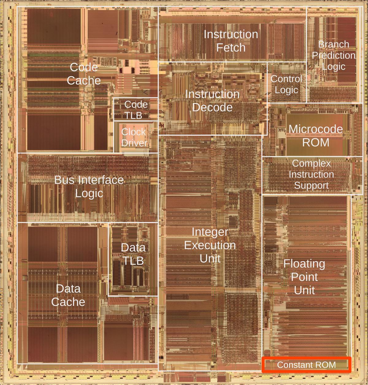
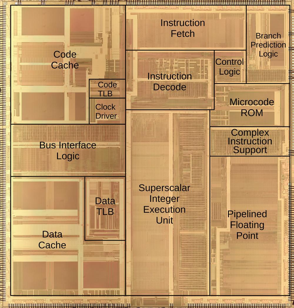
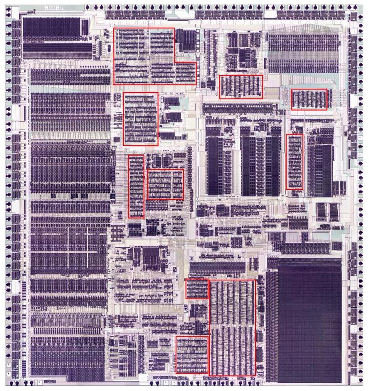
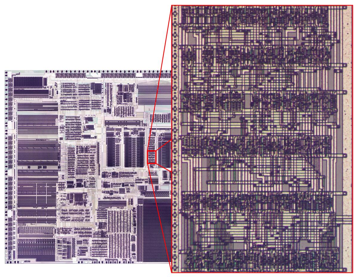
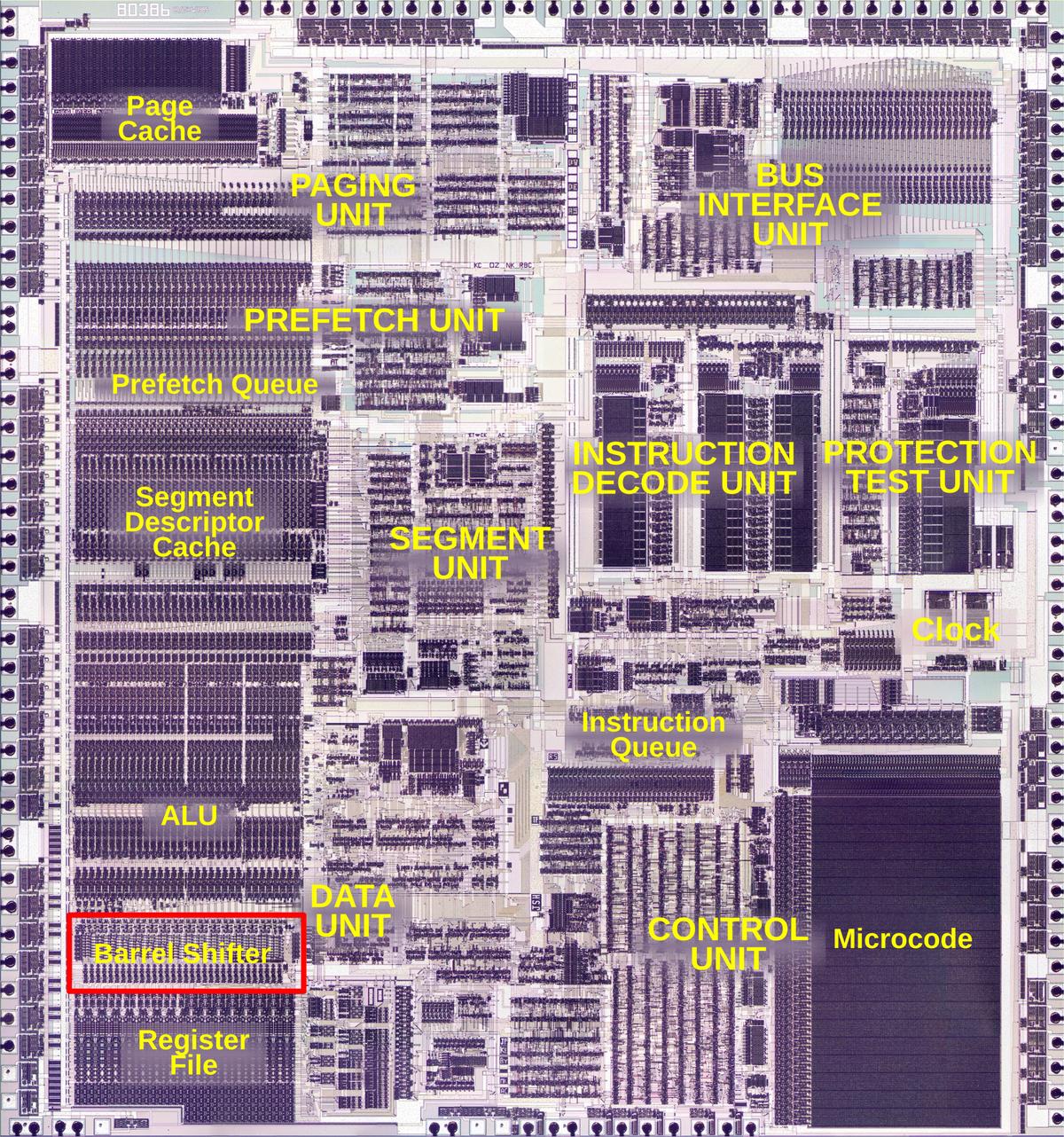
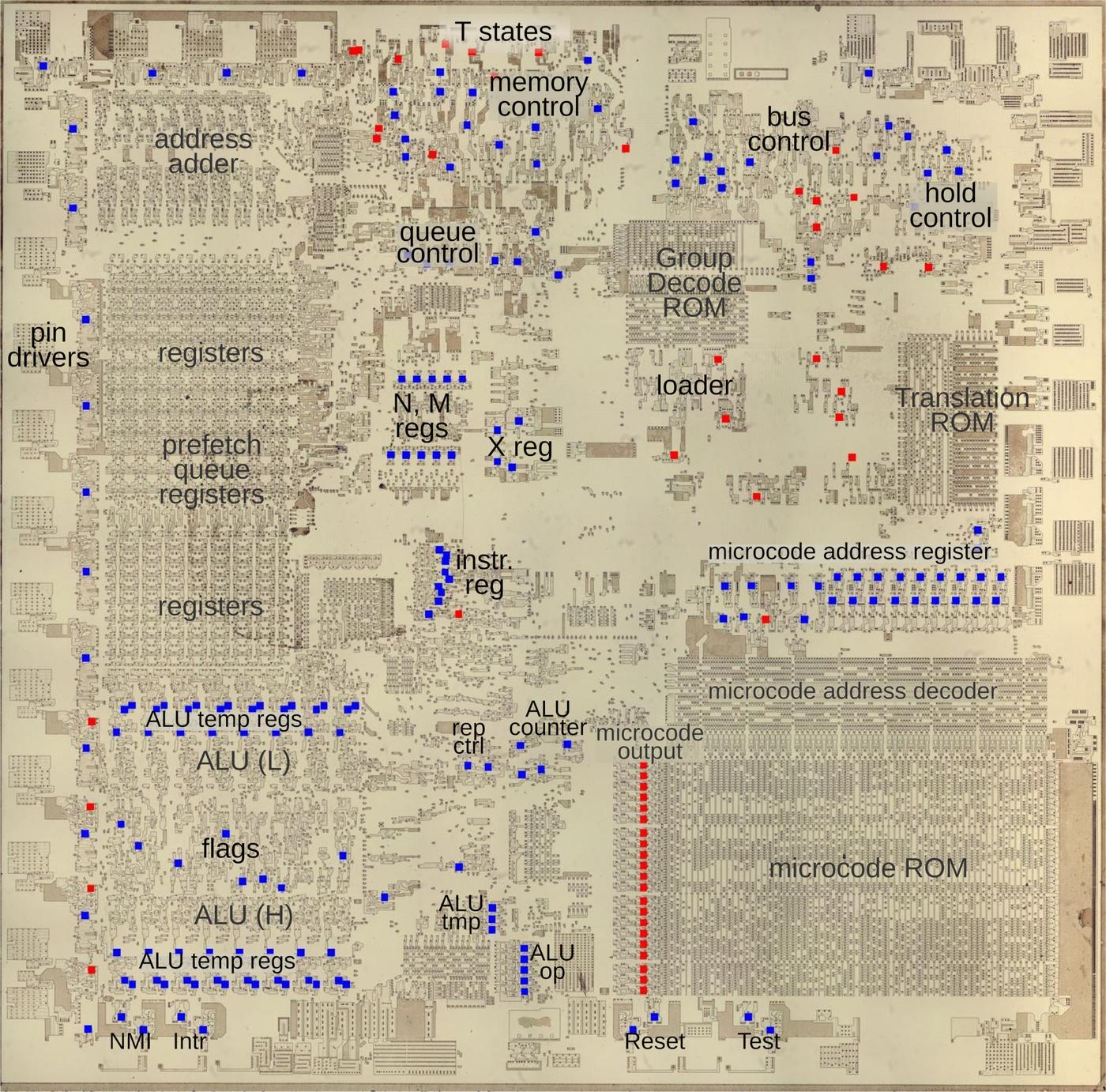
The photo below shows the Pentium's thumbnail-sized silicon die under a microscope. I've labeled the main functional blocks; the floating point unit is in the lower right with the constant ROM highlighted at the bottom. The various parts of the floating point unit form horizontal stripes. Data buses run vertically through the floating point unit, moving values around the unit.

Die photo of the Intel Pentium processor with the floating point constant ROM highlighted in red. Click this image (or any other) for a larger version.

Die photo of the Intel Pentium processor with the floating point constant ROM highlighted in red. Click this image (or any other) for a larger version.

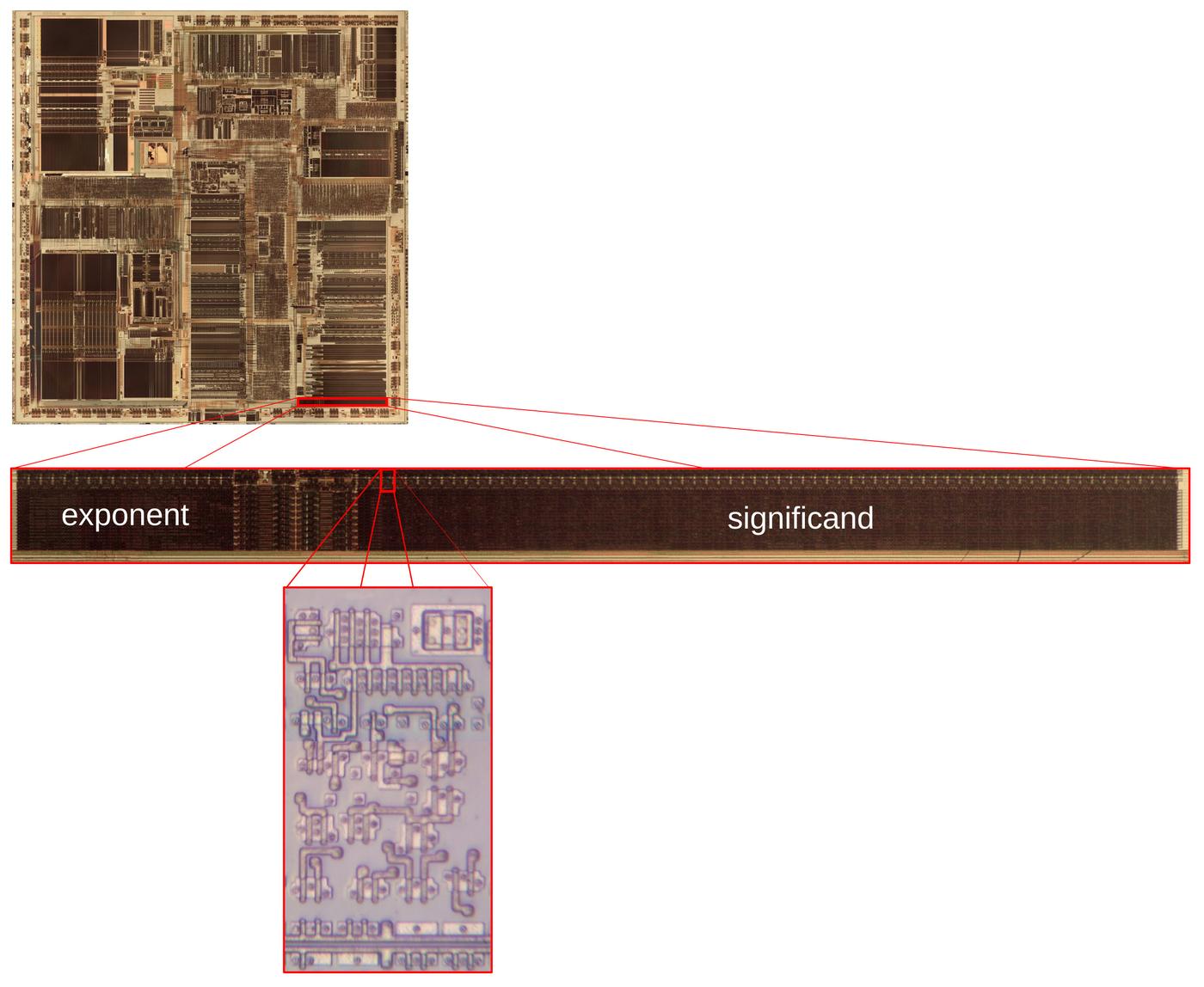
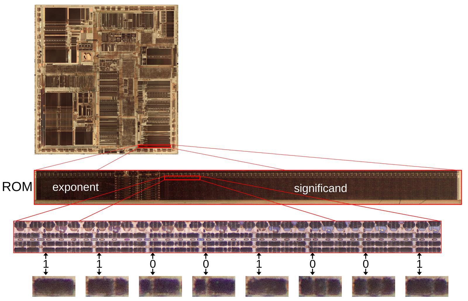
The diagram below shows how the circuitry in this post forms part of the Pentium. Zooming in to the bottom of the chip shows the constant ROM, holding 86-bit words: at the left, the exponent section provides 18 bits. At the right, the wider significand section provides 68 bits. Below that, the diagram zooms in on the subject of this article: one of the 86 identical multiplexer/driver circuits that provides the output from the ROM. As you can see, this circuit is a microscopic speck in the chip.

Zooming in on the constant ROM's driver circuits at the top of the ROM.

Zooming in on the constant ROM's driver circuits at the top of the ROM.

The layers

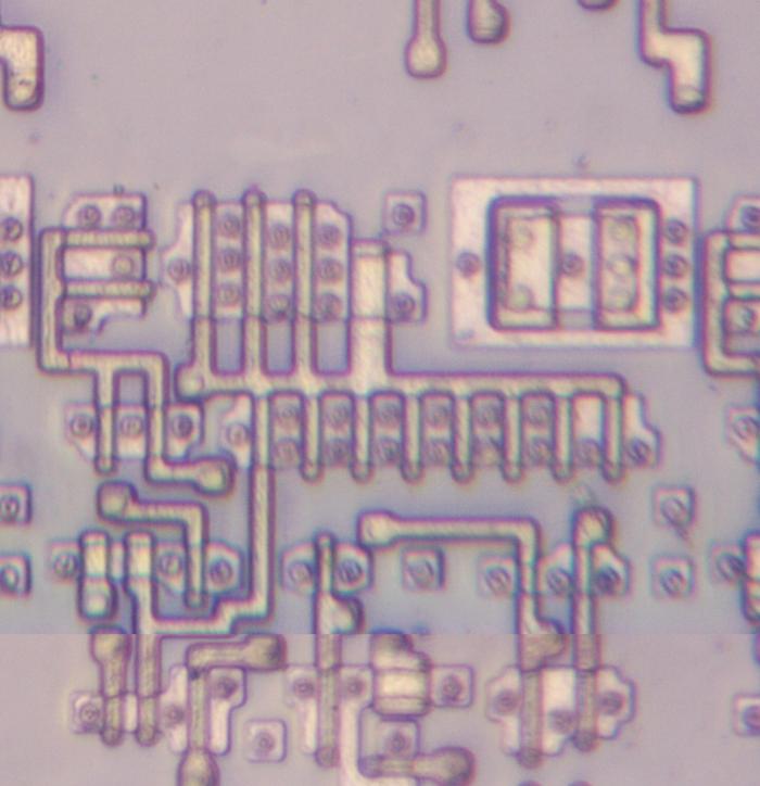
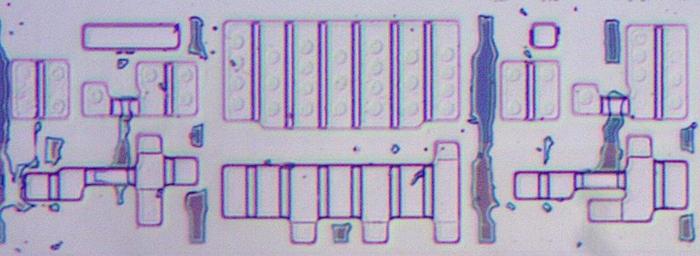
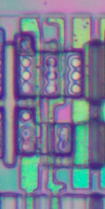
In this section, I'll show how the Pentium is constructed from layers. The bottom layer of the chip consists of transistors fabricated on the silicon die. Regions of silicon are doped with impurities to change the electrical properties; these regions appear pinkish in the photo below, compared to the grayish undoped silicon. Thin polysilicon wiring is formed on top of the silicon. Where a polysilicon line crosses doped silicon, a transistor is formed; the polysilicon creates the transistor's gate. Most of these transistors are NMOS and PMOS transistors, but there is a bipolar transistor near the upper right, the large box-like structure. The dark circles are contacts, regions where the metal layer above is connected to the polysilicon or silicon to wire the circuits together.

The polysilicon and silicon layers form the Pentium's transistors. This photo shows part of the complete circuit.

The polysilicon and silicon layers form the Pentium's transistors. This photo shows part of the complete circuit.

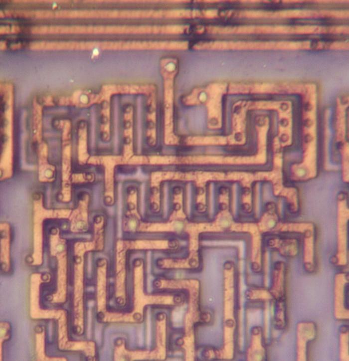
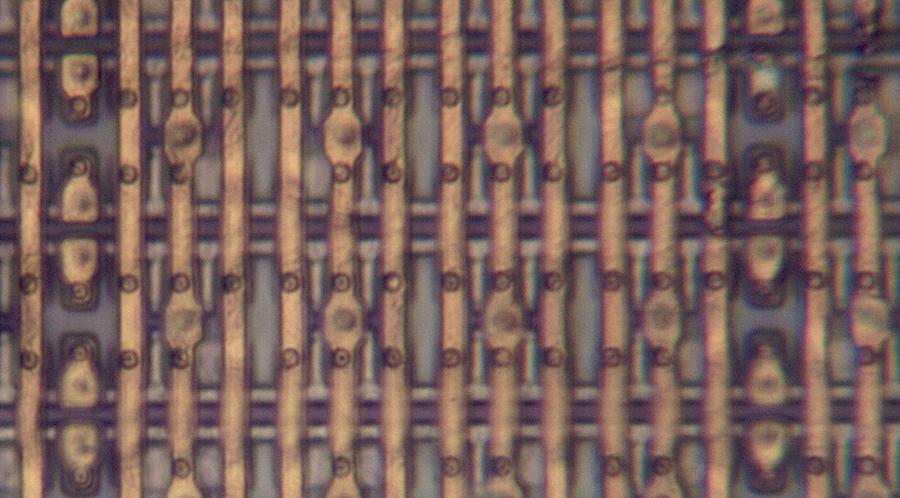
The Pentium has three layers of metal wiring. The photo below shows the bottom layer, called M1. For the most part, this layer of metal connects the transistors into various circuits, providing wiring over a short distance. The photos in this section show the same region of the chip, so you can match up features between the photos. For instance, the contacts below (black circles) match the black circles above, showing how this metal layer connects to the silicon and polysilicon circuits. You can see some of the silicon and polysilicon in this image, but most of it is hidden by the metal.

The Pentium's M1 metal layer is the bottom metal layer.

The Pentium's M1 metal layer is the bottom metal layer.

The M2 metal layer (below) sits above the M1 wiring. In this part of the chip, the M2 wires are horizontal. The thicker lines are power and ground. (Because they are thicker, they have lower resistance and can provide the necessary current to the underlying circuitry.) The thinner lines are control signals. The floating point unit is structured so functional blocks are horizontal, while data is transmitted vertically. Thus, a horizontal wire can supply a control signal to all the bits in a functional block.

The Pentium's M2 layer.

The Pentium's M2 layer.

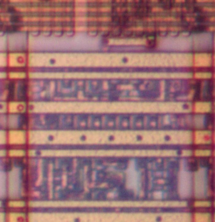
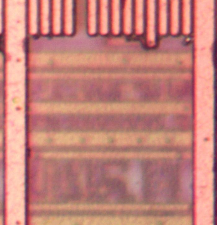
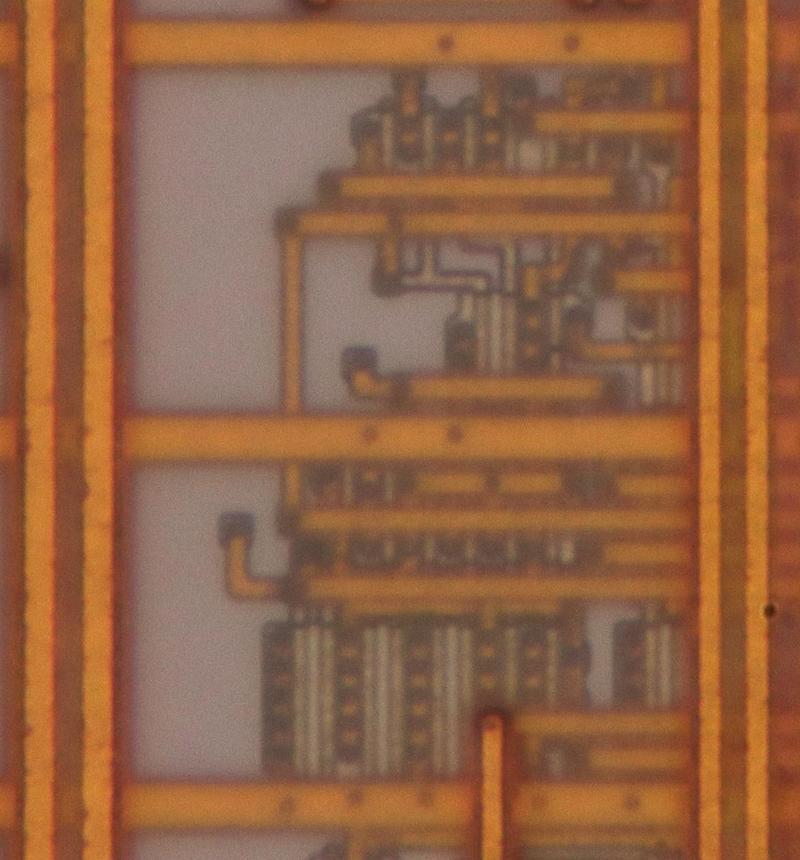
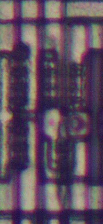
The M3 layer is the top metal layer in the Pentium. It is thicker, so it is better suited for the chip's main power and ground lines as well as long-distance bus wiring. In the photo below, the wide line on the left provides power, while the wide line on the right provides ground. The power and ground are distributed through wiring in the M2 and M1 layers until they are connected to the underlying transistors. At the top of the photo, vertical bus lines are visible; these extend for long distances through the floating point unit. Notice the slightly longer line, fourth from the right. This line provides one bit of data from the ROM, provided by the circuitry described below. The dot near the bottom is a via, connecting this line to a short wire in M2, connected to a wire in M1, connected to the silicon of the output transistors.

The Pentium's M3 metal layer. Lower layers are visible, but blurry due to the insulating oxide layers.

The Pentium's M3 metal layer. Lower layers are visible, but blurry due to the insulating oxide layers.

The circuits for the ROM's output

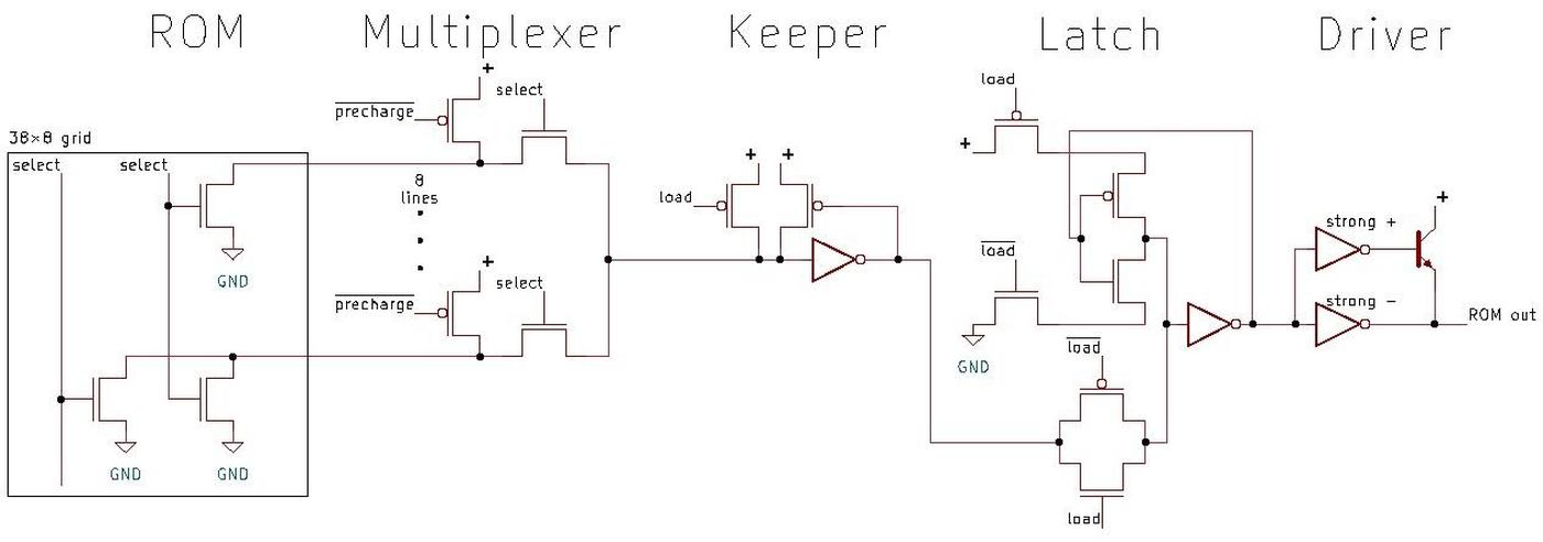
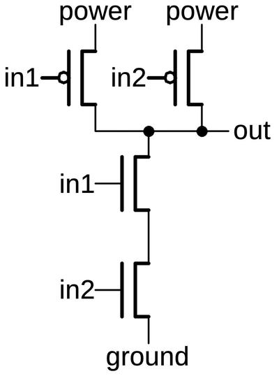
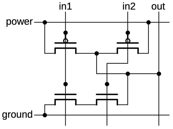
The simplified schematic below shows the circuit that I reverse-engineered. This circuit is repeated 86 times, once for each bit in the ROM's word. You might expect the ROM to provide a single 86-bit word. However, to make the layout work better, the ROM provides eight words in parallel. Thus, the circuitry must select one of the eight words with a multiplexer. In particular, each of the 86 circuits has an 8-to-1 multiplexer to select one bit out of the eight. This bit is then stored in a latch. Finally, a high-current driver amplifies the signal so it can be sent through a bus, traveling to a destination halfway across the floating point unit.

A high-level schematic of the circuit.

A high-level schematic of the circuit.

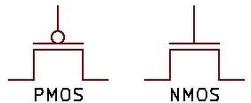
I'll provide a quick review of MOS transistors before I explain the circuitry in detail. CMOS circuitry uses two types of transistors—PMOS and NMOS—which are similar but also opposites. A PMOS transistor is turned on by a low signal on the gate, while an NMOS transistor is turned on by a high signal on the gate; the PMOS symbol has an inversion bubble on the gate. A PMOS transistor works best when pulling its output high, while an NMOS transistor works best when pulling its output low. CMOS circuitry normally uses the two types of MOS transistors in a Complementary fashion to implement logic gates, working together. What makes the circuits below interesting is that they often use NMOS and PMOS transistors independently.

The symbol for a PMOS transistor and an NMOS transistor.

The symbol for a PMOS transistor and an NMOS transistor.

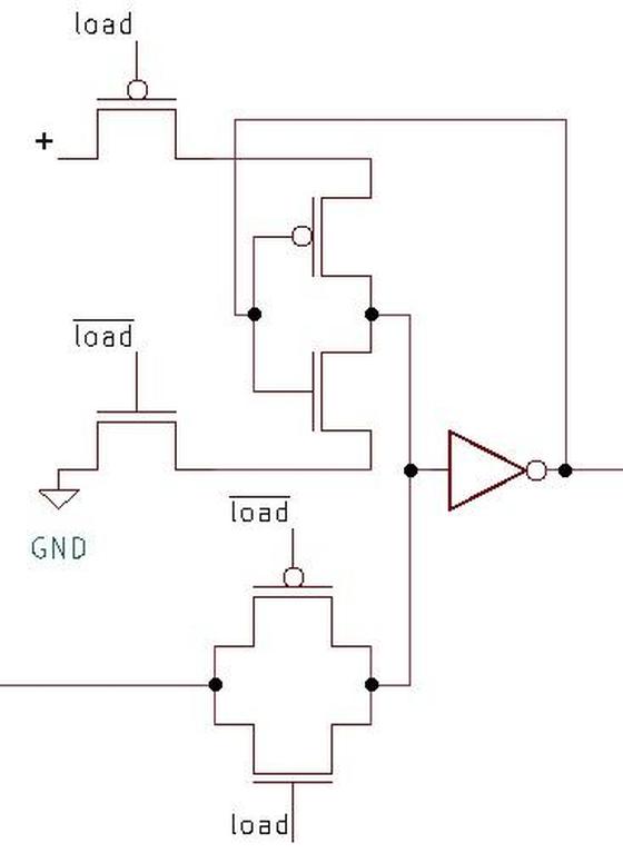
The detailed schematic below shows the circuitry at the transistor and inverter level. I'll go through each of the components in the remainder of this post.

A detailed schematic of the circuit. Click for a larger version.

A detailed schematic of the circuit. Click for a larger version.

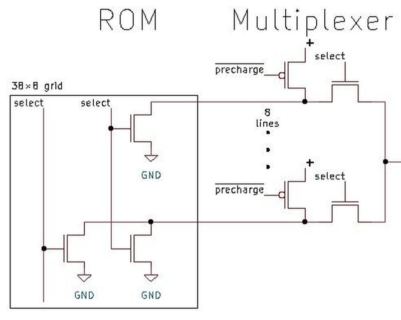
The ROM is constructed as a grid: at each grid point, the ROM can have a transistor for a 0 bit, or no transistor for a 1 bit. Thus, the data is represented by the transistor pattern. The ROM holds 304 constants so there are 304 potential transistors associated with each bit of the output word. These transistors are organized in a 38×8 grid. To select a word from the ROM, a select line activates one group of eight potential transistors. Each transistor is connected to ground, so the transistor (if present) will pull the associated line low, for a 0 bit. Note that the ROM itself consists of only NMOS transistors, making it half the size of a truly CMOS implementation. For more information on the structure and contents of the ROM, see my earlier article.

The ROM grid and multiplexer.

The ROM grid and multiplexer.

A ROM transistor can pull a line low for a 0 bit, but how does the line get pulled high for a 1 bit? This is accomplished by a precharge transistor on each line. Before a read from the ROM, the precharge transistors are all activated, pulling the lines high. If a ROM transistor is present on the line, the line will next be pulled low, but otherwise it will remain high due to the capacitance on the line.

Next, the multiplexer above selects one of the 8 lines, depending on which word is being accessed. The multiplexer consists of eight transistors. One transistor is activated by a select line, allowing the ROM's signal to pass through. The other seven transistors are in the off state, blocking those ROM signals. Thus, the multiplexer selects one of the 8 bits from the ROM.

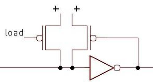
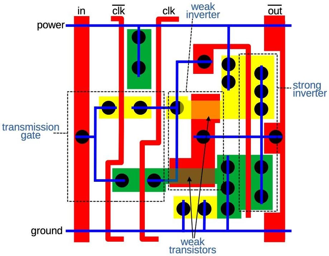
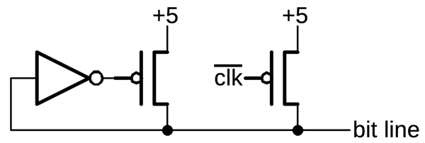
The circuit below is the "keeper." As explained above, each ROM line is charged high before reading the ROM. However, this charge can fade away. The job of the keeper is to keep the multiplexer's output high until it is pulled low. This is implemented by an inverter connected to a PMOS transistor. If the signal on the line is high, the PMOS transistor will turn on, pulling the line high. (Note that a PMOS transistor is turned on by a low signal, thus the inverter.) If the ROM pulls the line low, the transistor will turn off and stop pulling the line high. This transistor is very weak, so it is easily overpowered by the signal from the ROM. The transistor on the left ensures that the line is high at the start of the cycle.

The keeper circuit.

The keeper circuit.

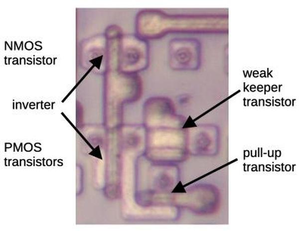
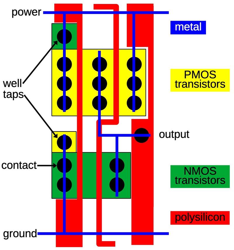
The diagram below shows the transistors for the keeper. The two transistors on the left implement a standard CMOS inverter. On the right, note the weak transistor that holds the line high. You might notice that the weak transistor looks larger and wonder why that makes the transistor weak rather than strong. The explanation is that the transistor is large in the "wrong" dimension. The current capacity of an MOS transistor is proportional to the width/length ratio of its gate. (Width is usually the long dimension and length is usually the skinny dimension.) The weak transistor's length is much larger than the other transistors, so the W/L ratio is smaller and the transistor is weaker. (You can think of the transistor's gate as a bridge between its two sides. A wide bridge with many lanes lets lots of traffic through. However, a long, single-lane bridge will slow down the traffic.)

The silicon implementation of the keeper.

The silicon implementation of the keeper.

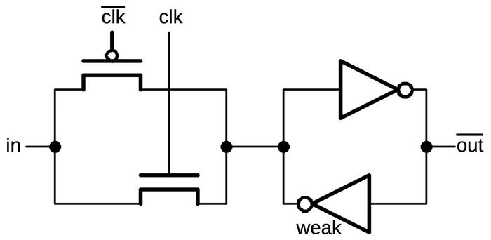
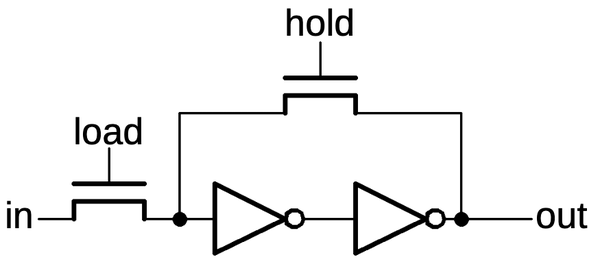
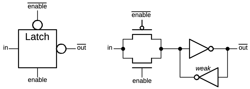
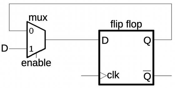
Next, we come to the latch, which remembers the value read from the ROM. This latch will read its input when the load signal is high. When the load signal goes low, the latch will hold its value. Conceptually, the latch is implemented with the circuit below. A multiplexer selects the lower input when the load signal is active, passing the latch input through to the (inverted) output. But when the load signal goes low, the multiplexer will select the top input, which is feedback of the value in the latch. This signal will cycle through the inverters and the multiplexer, holding the value until a new value is loaded. The inverters are required because the multiplexer itself doesn't provide any amplification; the signal would rapidly die out if not amplified by the inverters.

The implementation of the latch.

The implementation of the latch.

The multiplexer is implemented with two CMOS switches, one to select each multiplexer input. Each switch is a pair of PMOS and NMOS transistors that turn on together, allowing a signal to pass through. (See the bottom two transistors below.)1 The upper circuit is trickier. Conceptually, it is an inverter feeding into the multiplexer's CMOS switch. However, the order is switched so the switch feeds into the inverter. The result is not-exactly-a-switch and not-exactly-an-inverter, but the result is the same. You can also view it as an inverter with power and ground that gets cut off when not selected. I suspect this implementation uses slightly less power than the straightforward implementation.

The detailed schematic of the latch.

The detailed schematic of the latch.

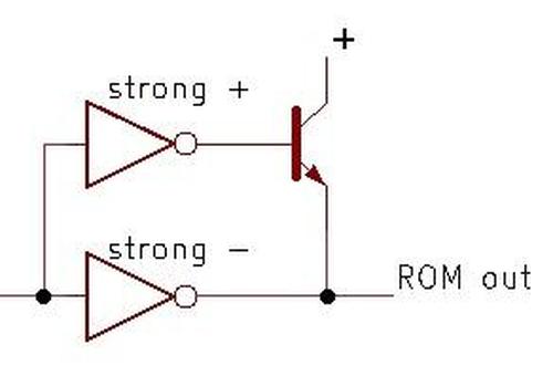
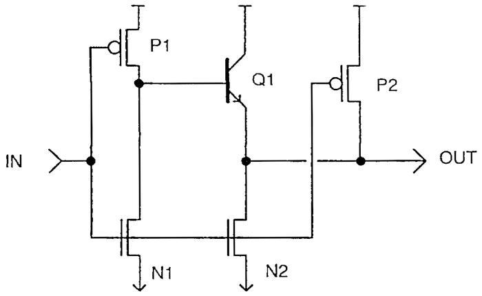
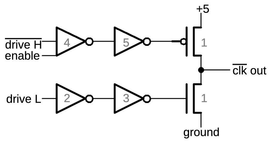
The most unusual circuit is the BiCMOS driver. By adding a few extra processing steps to the regular CMOS manufacturing process, bipolar (NPN and PNP) transistors can be created. The Pentium extensively used BiCMOS circuits since they reduced signal delays by up to 35%. Intel also used BiCMOS for the Pentium Pro, Pentium II, Pentium III, and Xeon processors. However, as chip voltages dropped, the benefit from bipolar transistors dropped too and BiCMOS was eventually abandoned.

The BiCMOS driver circuit.

The BiCMOS driver circuit.

In the Pentium, BiCMOS drivers are used when signals must travel a long distance across the chip. (In this case, the ROM output travels about halfway up the floating point unit.) These long wires have a lot of capacitance so a high-current driver circuit is needed and the NPN transistor provides extra "oomph."

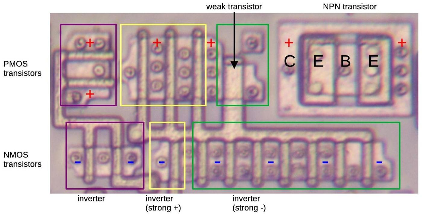
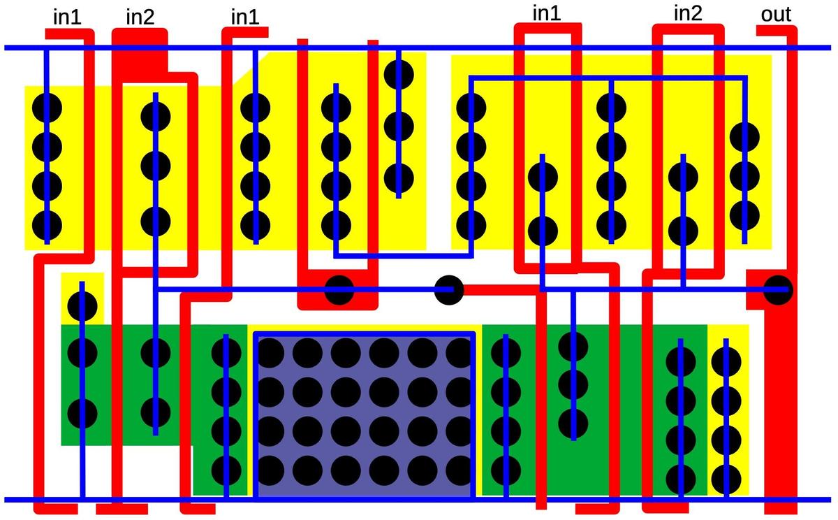
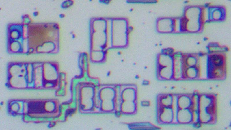
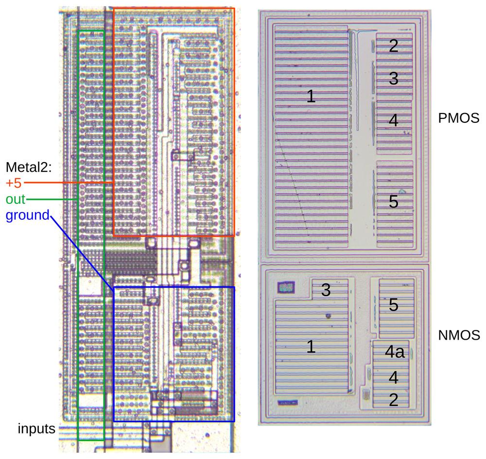
The diagram below shows how the driver is implemented. The NPN transistor is the large boxy structure in the upper right. When the base (B) is pulled high, current flows from the collector (C), pulling the emitter (E) high and thus rapidly pulling the output high. The remainder of the circuit consists of three inverters, each composed of PMOS and NMOS transistors. When a polysilicon line crosses doped silicon, it creates a transistor gate, so each crossing corresponds to a transistor. The inverters use multiple transistors in parallel to provide more current; the transistor sources and/or drains overlap to make the circuitry more compact.

This diagram shows the silicon and polysilicon for the driver circuit.

This diagram shows the silicon and polysilicon for the driver circuit.

One interesting thing about this circuit is that each inverter is carefully designed to provide the desired current, with a different current for a high output versus a low output. The first transistor (purple boxes) has two PMOS transistors and two NMOS transistors, so it is a regular inverter, balanced for high and low outputs. (This inverter is conceptually part of the latch.) The second inverter (yellow boxes) has three large PMOS transistors and one smaller NMOS transistor, so it has more ability to pull the output high than low. This transistor turns on the NPN transistor by providing a high signal to the base, so it needs more current in the high state. The third inverter (green boxes) has one weak PMOS transistor and seven NMOS transistors, so it can pull its output low strongly, but can barely pull its output high. This transistor pulls the ROM output line low, so it needs enough current to drive the entire bus line. But this transistor doesn't need to pull the output high—that's the job of the NPN transistor—so the PMOS transistor can be weak. The construction of the weak transistor is similar to the keeper's weak transistor; its gate length is much larger than the other transistors, so it provides less current.

Conclusions

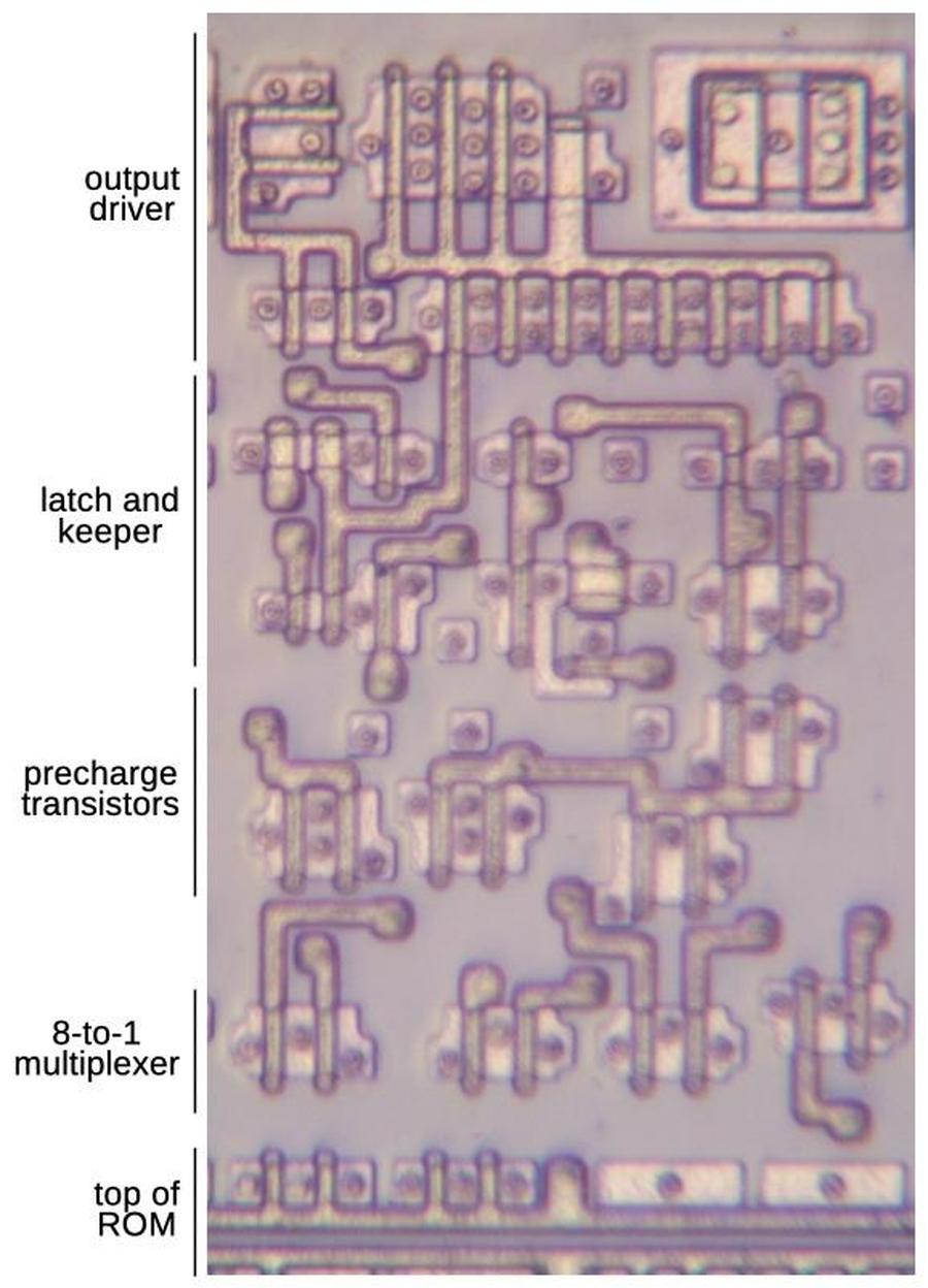
The diagram below shows how the functional blocks are arranged in the complete circuit, from the ROM at the bottom to the output at the top. The floating point unit is constructed with a constant width for each bit—38.5 µm—so the circuitry is designed to fit into this width. The layout of this circuitry was hand-optimized to fit as tightly as possible, In comparison, much of the Pentium's circuitry was arranged by software using a standard-cell approach, which is much easier to design but not as dense. Since each bit in the floating point unit is repeated many times, hand-optimization paid off here.

The silicon and polysilicon of the circuit, showing the functional blocks.

The silicon and polysilicon of the circuit, showing the functional blocks.

This circuit contains 47 transistors. Since it is duplicated once for each bit, it has 4042 transistors in total, a tiny fraction of the Pentium's 3.1 million transistors. In comparison, the MOS 6502 processor has about 3500-4500 transistors, depending on how you count. In other words, the circuit to select a word from the Pentium's ROM is about as complex as the entire 6502 processor. This illustrates the dramatic growth in processor complexity described by Moore's law.

I plan to write more about the Pentium so follow me on Bluesky (@righto.com) or RSS for updates. (I'm no longer on Twitter.) You might enjoy reading about the Pentium Navajo rug.

Notes

  1. The 8-to-1 multiplexer and the latch's multiplexer use different switch implementations: the first is built from NMOS transistors while the second is built from paired PMOS and NMOS transistors. The reason is that NMOS transistors are better at pulling signals low, while PMOS transistors are better at pulling signals high. Combining the transistors creates a switch that passes low and high signals efficiently, which is useful in the latch. The 8-to-1 multiplexer, however, only needs to pull signals low (due to the precharging), so the NMOS-only multiplexer works in this role. (Note that early NMOS processors like the 6502 and 8086 built multiplexers and pass-transistor logic out of solely NMOS. This illustrates that you can use NMOS-only switches with both logic levels, but performance is better if you add PMOS transistors.) 

Pi in the Pentium: reverse-engineering the constants in its floating-point unit

Intel released the powerful Pentium processor in 1993, establishing a long-running brand of high-performance processors.1 The Pentium includes a floating-point unit that can rapidly compute functions such as sines, cosines, logarithms, and exponentials. But how does the Pentium compute these functions? Earlier Intel chips used binary algorithms called CORDIC, but the Pentium switched to polynomials to approximate these transcendental functions much faster. The polynomials have carefully-optimized coefficients that are stored in a special ROM inside the chip's floating-point unit. Even though the Pentium is a complex chip with 3.1 million transistors, it is possible to see these transistors under a microscope and read out these constants. The first part of this post discusses how the floating point constant ROM is implemented in hardware. The second part explains how the Pentium uses these constants to evaluate sin, log, and other functions.

The photo below shows the Pentium's thumbnail-sized silicon die under a microscope. I've labeled the main functional blocks; the floating-point unit is in the lower right. The constant ROM (highlighted) is at the bottom of the floating-point unit. Above the floating-point unit, the microcode ROM holds micro-instructions, the individual steps for complex instructions. To execute an instruction such as sine, the microcode ROM directs the floating-point unit through dozens of steps to compute the approximation polynomial using constants from the constant ROM.

Die photo of the Intel Pentium processor with the floating point constant ROM highlighted in red. Click this image (or any other) for a larger version.

Die photo of the Intel Pentium processor with the floating point constant ROM highlighted in red. Click this image (or any other) for a larger version.

Finding pi in the constant ROM

In binary, pi is 11.00100100001111110... but what does this mean? To interpret this, the value 11 to the left of the binary point is simply 3 in binary. (The "binary point" is the same as a decimal point, except for binary.) The digits to the right of the binary point have the values 1/2, 1/4, 1/8, and so forth. Thus, the binary value `11.001001000011... corresponds to 3 + 1/8 + 1/64 + 1/4096 + 1/8192 + ..., which matches the decimal value of pi. Since pi is irrational, the bit sequence is infinite and non-repeating; the value in the ROM is truncated to 67 bits and stored as a floating point number.

A floating point number is represented by two parts: the exponent and the significand. Floating point numbers include very large numbers such as 6.02×10²³ and very small numbers such as 1.055×10⁻³⁴. In decimal, 6.02×10²³ has a significand (or mantissa) of 6.02, multiplied by a power of 10 with an exponent of 23. In binary, a floating point number is represented similarly, with a significand and exponent, except the significand is multiplied by a power of 2 rather than 10. For example, pi is represented in floating point as 1.1001001...×21.

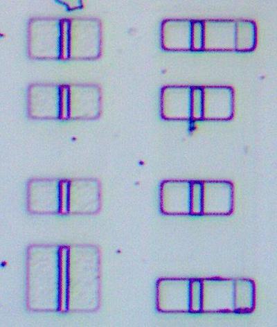
The diagram below shows how pi is encoded in the Pentium chip. Zooming in shows the constant ROM. Zooming in on a small part of the ROM shows the rows of transistors that store the constants. The arrows point to the transistors representing the bit sequence 11001001, where a 0 bit is represented by a transistor (vertical white line) and a 1 bit is represented by no transistor (solid dark silicon). Each magnified black rectangle at the bottom has two potential transistors, storing two bits. The key point is that by looking at the pattern of stripes, we can determine the pattern of transistors and thus the value of each constant, pi in this case.

A portion of the floating-point ROM, showing the value of pi. Click this image (or any other) for a larger version.

A portion of the floating-point ROM, showing the value of pi. Click this image (or any other) for a larger version.

The bits are spread out because each row of the ROM holds eight interleaved constants to improve the layout. Above the ROM bits, multiplexer circuitry selects the desired constant from the eight in the activated row. In other words, by selecting a row and then one of the eight constants in the row, one of the 304 constants in the ROM is accessed. The ROM stores many more digits of pi than shown here; the diagram shows 8 of the 67 significand bits.

Implementation of the constant ROM

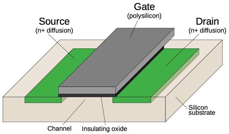
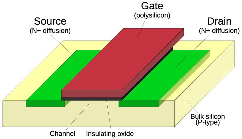
The ROM is built from MOS (metal-oxide-semiconductor) transistors, the transistors used in all modern computers. The diagram below shows the structure of an MOS transistor. An integrated circuit is constructed from a silicon substrate. Regions of the silicon are doped with impurities to create "diffusion" regions with desired electrical properties. The transistor can be viewed as a switch, allowing current to flow between two diffusion regions called the source and drain. The transistor is controlled by the gate, made of a special type of silicon called polysilicon. Applying voltage to the gate lets current flow between the source and drain, which is otherwise blocked. Most computers use two types of MOS transistors: NMOS and PMOS. The two types have similar construction but reverse the doping; NMOS uses n-type diffusion regions as shown below, while PMOS uses p-type diffusion regions. Since the two types are complementary (C), circuits built with the two types of transistors are called CMOS.

Structure of a MOSFET in an integrated circuit.

Structure of a MOSFET in an integrated circuit.

The image below shows how a transistor in the ROM looks under the microscope. The pinkish regions are the doped silicon that forms the transistor's source and drain. The vertical white line is the polysilicon that forms the transistor's gate. For this photo, I removed the chip's three layers of metal, leaving just the underlying silicon and the polysilicon. The circles in the source and drain are tungsten contacts that connect the silicon to the metal layer above.

One transistor in the constant ROM.

One transistor in the constant ROM.

The diagram below shows eight bits of storage. Each of the four pink silicon rectangles has two potential transistors. If a polysilicon gate crosses the silicon, a transistor is formed; otherwise there is no transistor. When a select line (horizontal polysilicon) is energized, it will turn on all the transistors in that row. If a transistor is present, the corresponding ROM bit is 0 because the transistor will pull the output line to ground. If a transistor is absent, the ROM bit is 1. Thus, the pattern of transistors determines the data stored in the ROM. The ROM holds 26144 bits (304 words of 86 bits) so it has 26144 potential transistors.

Eight bits of storage in the ROM.

Eight bits of storage in the ROM.

The photo below shows the bottom layer of metal (M1): vertical metal wires that provide the ROM outputs and supply ground to the ROM. (These wires are represented by gray lines in the schematic above.) The polysilicon transistors (or gaps as appropriate) are barely visible between the metal lines. Most of the small circles are tungsten contacts to the silicon or polysilicon; compare with the photo above. Other circles are tungsten vias to the metal layer on top (M2), horizontal wiring that I removed for this photo. The smaller metal "tabs" act as jumpers between the horizontal metal select lines in M2 and the polysilicon select lines. The top metal layer (M3, not visible) has thicker vertical wiring for the chip's primary distribution power and ground. Thus, the three metal layers alternate between horizontal and vertical wiring, with vias between the layers.

A closeup of the ROM showing the bottom metal layer.

A closeup of the ROM showing the bottom metal layer.

The ROM is implemented as two grids of cells (below): one to hold exponents and one to hold significands, as shown below. The exponent grid (on the left) has 38 rows and 144 columns of transistors, while the significand grid (on the right) has 38 rows and 544 columns. To make the layout work better, each row holds eight different constants; the bits are interleaved so the ROM holds the first bit of eight constants, then the second bit of eight constants, and so forth. Thus, with 38 rows, the ROM holds 304 constants; each constant has 18 bits in the exponent part and 68 bits in the significand section.

A diagram of the constant ROM and supporting circuitry. Most of the significand ROM has been cut out to make it fit.

A diagram of the constant ROM and supporting circuitry. Most of the significand ROM has been cut out to make it fit.

The exponent part of each constant consists of 18 bits: a 17-bit exponent and one bit for the sign of the significand and thus the constant. There is no sign bit for the exponent because the exponent is stored with 65535 (0x0ffff) added to it, avoiding negative values. The 68-bit significand entry in the ROM consists of a mysterious flag bit2 followed by the 67-bit significand; the first bit of the significand is the integer part and the remainder is the fractional part.3 The complete contents of the ROM are in the appendix at the bottom of this post.

To select a particular constant, the "row select" circuitry between the two sections activates one of the 38 rows. That row provides 144+544 bits to the selection circuitry above the ROM. This circuitry has 86 multiplexers; each multiplexer selects one bit out of the group of 8, selecting the desired constant. The significand bits flow into the floating-point unit datapath circuitry above the ROM. The exponent circuitry, however, is in the upper-left corner of the floating-point unit, a considerable distance from the ROM, so the exponent bits travel through a bus to the exponent circuitry.

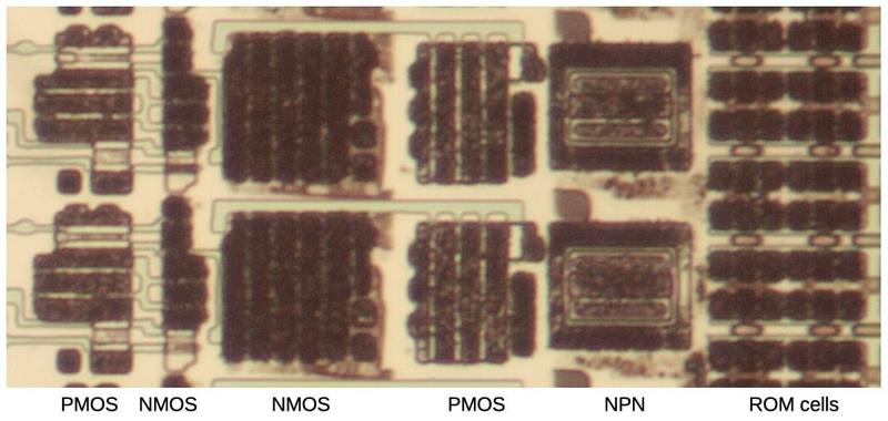
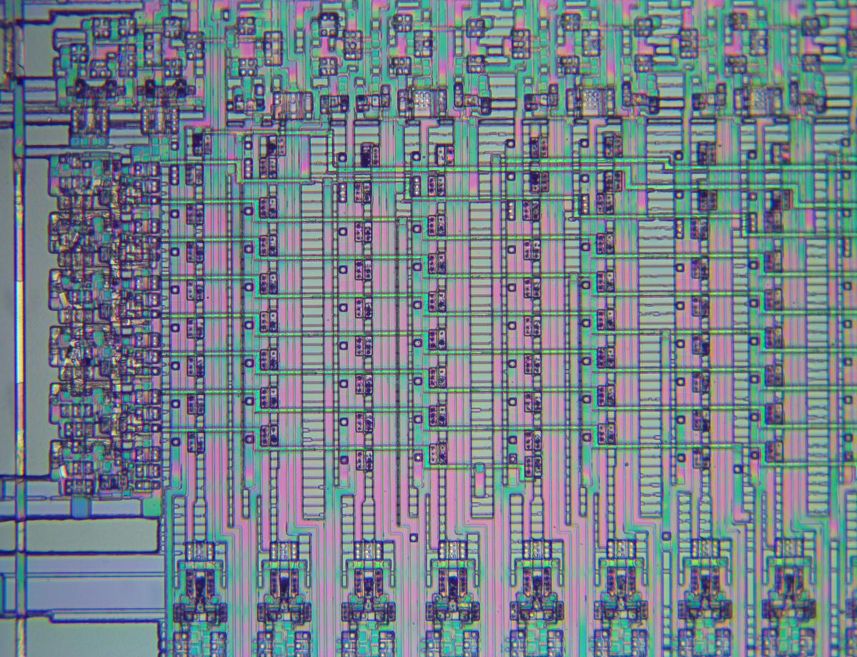
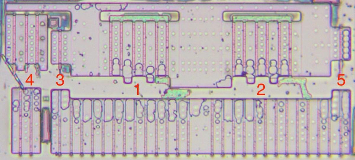
The row select circuitry consists of gates to decode the row number, along with high-current drivers to energize the selected row in the ROM. The photo below shows a closeup of two row driver circuits, next to some ROM cells. At the left, PMOS and NMOS transistors implement a gate to select the row. Next, larger NMOS and PMOS transistors form part of the driver. The large square structures are bipolar NPN transistors; the Pentium is unusual because it uses both bipolar transistors and CMOS, a technique called BiCMOS.4 Each driver occupies as much height as four rows of the ROM, so there are four drivers arranged horizontally; only one is visible in the photo.

ROM drivers implemented with BiCMOS.

ROM drivers implemented with BiCMOS.

Structure of the floating-point unit

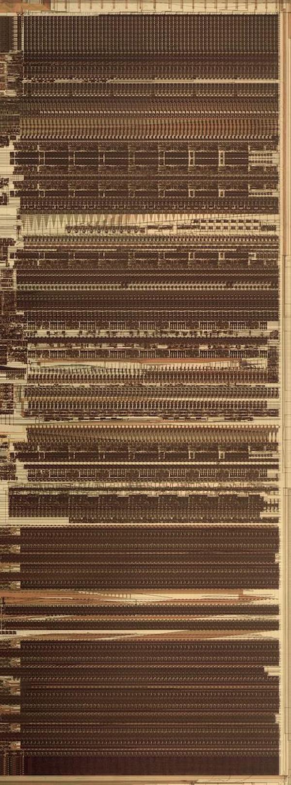
The floating-point unit is structured with data flowing vertically through horizontal functional units, as shown below. The functional units—adders, shifters, registers, and comparators—are arranged in rows. This collection of functional units with data flowing through them is called the datapath.5

The datapath of the floating-point unit. The ROM is at the bottom.

The datapath of the floating-point unit. The ROM is at the bottom.

Each functional unit is constructed from cells, one per bit, with the high-order bit on the left and the low-order bit on the right. Each cell has the same width—38.5 µm—so the functional units can be connected like Lego blocks snapping together, minimizing the wiring. The height of a functional unit varies as needed, depending on the complexity of the circuit. Functional units typically have 69 bits, but some are wider, so the edges of the datapath circuitry are ragged.

This cell-based construction explains why the ROM has eight constants per row. A ROM bit requires a single transistor, which is much narrower than, say, an adder. Thus, putting one bit in each 38.5 µm cell would waste most of the space. Compacting the ROM bits into a narrow block would also be inefficient, requiring diagonal wiring to connect each ROM bit to the corresponding datapath bit. By putting eight bits for eight different constants into each cell, the width of a ROM cell matches the rest of the datapath and the alignment of bits is preserved. Thus, the layout of the ROM in silicon is dense, efficient, and matches the width of the rest of the floating-point unit.

Polynomial approximation: don't use a Taylor series

Now I'll move from the hardware to the constants. If you look at the constant ROM contents in the appendix, you may notice that many constants are close to reciprocals or reciprocal factorials, but don't quite match. For instance, one constant is 0.1111111089, which is close to 1/9, but visibly wrong. Another constant is almost 1/13! (factorial) but wrong by 0.1%. What's going on?

The Pentium uses polynomials to approximate transcendental functions (sine, cosine, tangent, arctangent, and base-2 powers and logarithms). Intel's earlier floating-point units, from the 8087 to the 486, used an algorithm called CORDIC that generated results a bit at a time. However, the Pentium takes advantage of its fast multiplier and larger ROM and uses polynomials instead, computing results two to three times faster than the 486 algorithm.

You may recall from calculus that a Taylor series polynomial approximates a function near a point (typically 0). For example, the equation below gives the Taylor series for sine.

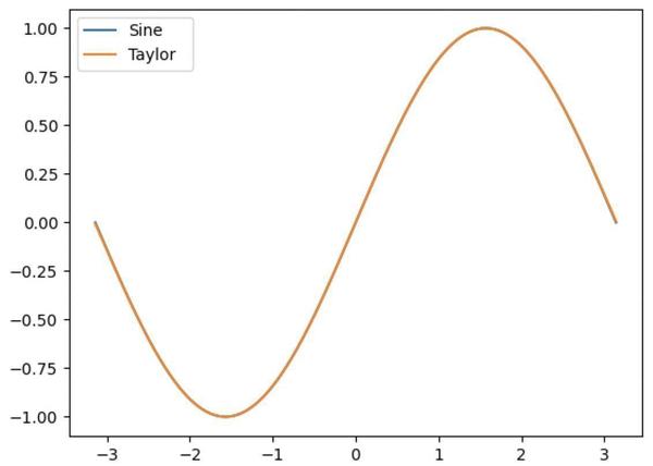
Using the five terms shown above generates a function that looks indistinguishable from sine in the graph below. However, it turns out that this approximation has too much error to be useful.

Plot of the sine function and the Taylor series approximation.

Plot of the sine function and the Taylor series approximation.

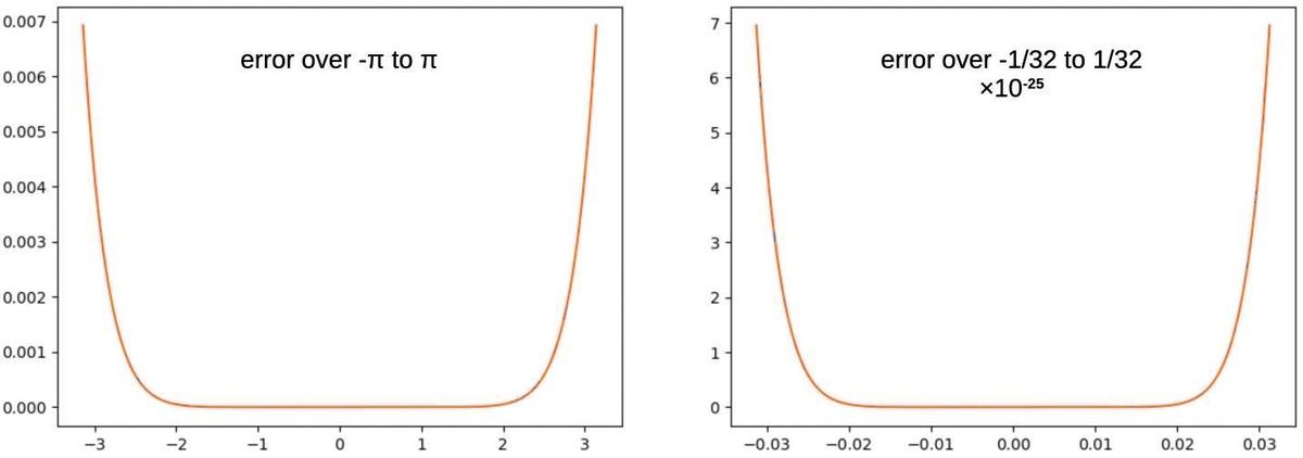
The problem is that a Taylor series is very accurate near 0, but the error soars near the edges of the argument range, as shown in the graph on the left below. When implementing a function, we want the function to be accurate everywhere, not just close to 0, so the Taylor series isn't good enough.

The absolute error for a Taylor-series approximation to sine (5 terms), over two different argument ranges.

The absolute error for a Taylor-series approximation to sine (5 terms), over two different argument ranges.

One improvement is called range reduction: shrinking the argument to a smaller range so you're in the accurate flat part.6 The graph on the right looks at the Taylor series over the smaller range [-1/32, 1/32]. This decreases the error dramatically, by about 22 orders of magnitude (note the scale change). However, the error still shoots up at the edges of the range in exactly the same way. No matter how much you reduce the range, there is almost no error in the middle, but the edges have a lot of error.7

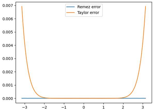
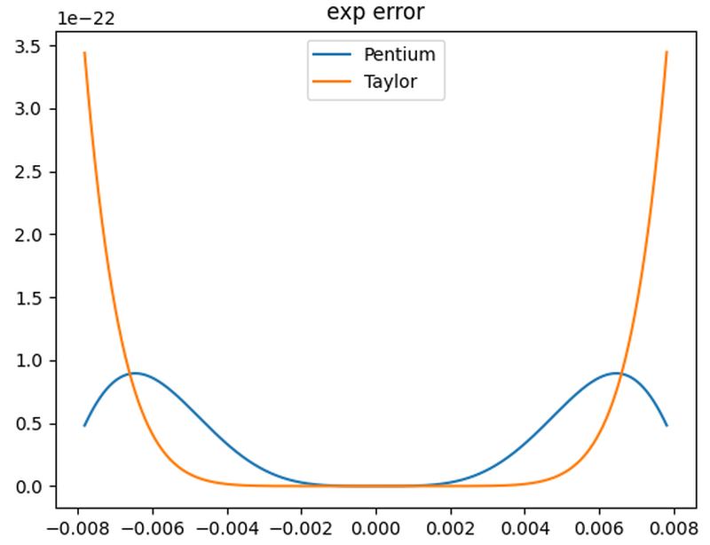
How can we get rid of the error near the edges? The trick is to tweak the coefficients of the Taylor series in a special way that will increase the error in the middle, but decrease the error at the edges by much more. Since we want to minimize the maximum error across the range (called minimax), this tradeoff is beneficial. Specifically, the coefficients can be optimized by a process called the Remez algorithm.8 As shown below, changing the coefficients by less than 1% dramatically improves the accuracy. The optimized function (blue) has much lower error over the full range, so it is a much better approximation than the Taylor series (orange).

Comparison of the absolute error from the Taylor series and a Remez-optimized polynomial, both with maximum term x9. This Remez polynomial is not one from the Pentium.

Comparison of the absolute error from the Taylor series and a Remez-optimized polynomial, both with maximum term x9. This Remez polynomial is not one from the Pentium.

To summarize, a Taylor series is useful in calculus, but shouldn't be used to approximate a function. You get a much better approximation by modifying the coefficients very slightly with the Remez algorithm. This explains why the coefficients in the ROM almost, but not quite, match a Taylor series.

Arctan

I'll now look at the Pentium's constants for different transcendental functions. The constant ROM contains coefficients for two arctan polynomials, one for single precision and one for double precision. These polynomials almost match the Taylor series, but have been modified for accuracy. The ROM also holds the values for arctan(1/32) through arctan(32/32); the range reduction process uses these constants with a trig identity to reduce the argument range to [-1/64, 1/64].9 You can see the arctan constants in the Appendix.

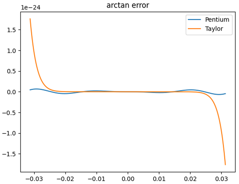
The graph below shows the error for the Pentium's arctan polynomial (blue) versus the Taylor series of the same length (orange). The Pentium's polynomial is superior due to the Remez optimization. Although the Taylor series polynomial is much flatter in the middle, the error soars near the boundary. The Pentium's polynomial wiggles more but it maintains a low error across the whole range. The error in the Pentium polynomial blows up outside this range, but that doesn't matter.

Comparison of the Pentium's double-precision arctan polynomial to the Taylor series.

Comparison of the Pentium's double-precision arctan polynomial to the Taylor series.

Trig functions

Sine and cosine each have two polynomial implementations, one with 4 terms in the ROM and one with 6 terms in the ROM. (Note that coefficients of 1 are not stored in the ROM.) The constant table also holds 16 constants such as sin(36/64) and cos(18/64) that are used for argument range reduction.10 The Pentium computes tangent by dividing the sine by the cosine. I'm not showing a graph because the Pentium's error came out worse than the Taylor series, so either I have an error in a coefficient or I'm doing something wrong.

Exponential

The Pentium has an instruction to compute a power of two.11 There are two sets of polynomial coefficients for exponential, one with 6 terms in the ROM and one with 11 terms in the ROM. Curiously, the polynomials in the ROM compute ex, not 2x. Thus, the Pentium must scale the argument by ln(2), a constant that is in the ROM. The error graph below shows the advantage of the Pentium's polynomial over the Taylor series polynomial.

The Pentium's 6-term exponential polynomial, compared with the Taylor series.

The Pentium's 6-term exponential polynomial, compared with the Taylor series.

The polynomial handles the narrow argument range [-1/128, 1/128]. Observe that when computing a power of 2 in binary, exponentiating the integer part of the argument is trivial, since it becomes the result's exponent. Thus, the function only needs to handle the range [1, 2]. For range reduction, the constant ROM holds 64 values of the form 2n/128-1. To reduce the range from [1, 2] to [-1/128, 1/128], the closest n/128 is subtracted from the argument and then the result is multiplied by the corresponding constant in the ROM. The constants are spaced irregularly, presumably for accuracy; some are in steps of 4/128 and others are in steps of 2/128.

Logarithm

The Pentium can compute base-2 logarithms.12 The coefficients define polynomials for the hyperbolic arctan, which is closely related to log. See the comments for details. The ROM also has 64 constants for range reduction: log2(1+n/64) for odd n from 1 to 63. The unusual feature of these constants is that each constant is split into two pieces to increase the bits of accuracy: the top part has 40 bits of accuracy and the bottom part has 67 bits of accuracy, providing a 107-bit constant in total. The extra bits are required because logarithms are hard to compute accurately.

Other constants

The x87 floating-point instruction set provides direct access to a handful of constants—0, 1, pi, log2(10), log2(e), log10(2), and loge(2)—so these constants are stored in the ROM. (These logs are useful for changing the base for logs and exponentials.) The ROM holds other constants for internal use by the floating-point unit such as -1, 2, 7/8, 9/8, pi/2, pi/4, and 2log2(e). The ROM also holds bitmasks for extracting part of a word, for instance accessing 4-bit BCD digits in a word. Although I can interpret most of the values, there are a few mysteries such as a mask with the inscrutable value 0x3e8287c. The ROM has 34 unused entries at the end; these entries hold words that include the descriptive hex value 0xbad or perhaps 0xbadfc for "bad float constant".

How I examined the ROM

To analyze the Pentium, I removed the metal and oxide layers with various chemicals (sulfuric acid, phosphoric acid, Whink). (I later discovered that simply sanding the die works surprisingly well.) Next, I took many photos of the ROM with a microscope. The feature size of this Pentium is 800 nm, just slightly larger than visible light (380-700 nm). Thus, the die can be examined under an optical microscope, but it is getting close to the limits. To determine the ROM contents, I tediously went through the ROM images, examining each of the 26144 bits and marking each transistor. After figuring out the ROM format, I wrote programs to combine simple functions in many different combinations to determine the mathematical expression such as arctan(19/32) or log2(10). Because the polynomial constants are optimized and my ROM data has bit errors, my program needed checks for inexact matches, both numerically and bitwise. Finally, I had to determine how the constants would be used in algorithms.

Conclusions

By examining the Pentium's floating-point ROM under a microscope, it is possible to extract the 304 constants stored in the ROM. I was able to determine the meaning of most of these constants and deduce some of the floating-point algorithms used by the Pentium. These constants illustrate how polynomials can efficiently compute transcendental functions. Although Taylor series polynomials are well known, they are surprisingly inaccurate and should be avoided. Minor changes to the coefficients through the Remez algorithm, however, yield much better polynomials.

In a previous article, I examined the floating-point constants stored in the 8087 coprocessor. The Pentium has 304 constants in the Pentium, compared to just 42 in the 8087, supporting more efficient algorithms. Moreover, the 8087 was an external floating-point unit, while the Pentium's floating-point unit is part of the processor. The changes between the 8087 (1980, 65,000 transistors) and the Pentium (1993, 3.1 million transistors) are due to the exponential improvements in transistor count, as described by Moore's Law.

I plan to write more about the Pentium so follow me on Bluesky (@righto.com) or RSS for updates. (I'm no longer on Twitter.) I've also written about the Pentium division bug and the Pentium Navajo rug. Thanks to CuriousMarc for microscope help. Thanks to lifthrasiir and Alexia for identifying some constants.

Appendix: The constant ROM

The table below lists the 304 constants in the Pentium's floating-point ROM. The first four columns show the values stored in the ROM: the exponent, the sign bit, the flag bit, and the significand. To avoid negative exponents, exponents are stored with the constant 0x0ffff added. For example, the value 0x0fffe represents an exponent of -1, while 0x10000 represents an exponent of 1. The constant's approximate decimal value is in the "value" column.

Special-purpose values are colored. Specifically, "normal" numbers are in black. Constants with an exponent of all 0's are in blue, constants with an exponent of all 1's are in red, constants with an unusually large or small exponent are in green; these appear to be bitmasks rather than numbers. Unused entries are in gray. Inexact constants (due to Remez optimization) are represented with the approximation symbol "≈".

This information is from my reverse engineering, so there will be a few errors.

expSFsignificandvaluemeaning
0 00000 0 0 07878787878787878 BCD mask by 4's
1 00000 0 0 007f807f807f807f8 BCD mask by 8's
2 00000 0 0 00007fff80007fff8 BCD mask by 16's
3 00000 0 0 000000007fffffff8 BCD mask by 32's
4 00000 0 0 78000000000000000 4-bit mask
5 00000 0 0 18000000000000000 2-bit mask
6 00000 0 0 27000000000000000 ?
7 00000 0 0 363c0000000000000 ?
8 00000 0 0 3e8287c0000000000 ?
9 00000 0 0 470de4df820000000 213×1016
10 00000 0 0 5c3bd5191b525a249 2123/1017
11 00000 0 0 00000000000000007 3-bit mask
12 1ffff 1 1 7ffffffffffffffff all 1's
13 00000 0 0 0000007ffffffffff mask for 32-bit float
14 00000 0 0 00000000000003fff mask for 64-bit float
15 00000 0 0 00000000000000000 all 0's
16 0ffff 0 0 40000000000000000  1 1
17 10000 0 0 6a4d3c25e68dc57f2  3.3219280949 log2(10)
18 0ffff 0 0 5c551d94ae0bf85de  1.4426950409 log2(e)
19 10000 0 0 6487ed5110b4611a6  3.1415926536 pi
20 0ffff 0 0 6487ed5110b4611a6  1.5707963268 pi/2
21 0fffe 0 0 6487ed5110b4611a6  0.7853981634 pi/4
22 0fffd 0 0 4d104d427de7fbcc5  0.3010299957 log10(2)
23 0fffe 0 0 58b90bfbe8e7bcd5f  0.6931471806 ln(2)
24 1ffff 0 0 40000000000000000 +infinity
25 0bfc0 0 0 40000000000000000 1/4 of smallest 80-bit denormal?
26 1ffff 1 0 60000000000000000 NaN (not a number)
27 0ffff 1 0 40000000000000000 -1 -1
28 10000 0 0 40000000000000000  2 2
29 00000 0 0 00000000000000001 low bit
30 00000 0 0 00000000000000000 all 0's
31 00001 0 0 00000000000000000 single exponent bit
32 0fffe 0 0 58b90bfbe8e7bcd5e  0.6931471806 ln(2)
33 0fffe 0 0 40000000000000000  0.5 1/2! (exp Taylor series)
34 0fffc 0 0 5555555555555584f  0.1666666667 ≈1/3!
35 0fffa 0 0 555555555397fffd4  0.0416666667 ≈1/4!
36 0fff8 0 0 444444444250ced0c  0.0083333333 ≈1/5!
37 0fff5 0 0 5b05c3dd3901cea50  0.0013888934 ≈1/6!
38 0fff2 0 0 6806988938f4f2318  0.0001984134 ≈1/7!
39 0fffe 0 0 40000000000000000  0.5 1/2! (exp Taylor series)
40 0fffc 0 0 5555555555555558e  0.1666666667 ≈1/3!
41 0fffa 0 0 5555555555555558b  0.0416666667 ≈1/4!
42 0fff8 0 0 444444444443db621  0.0083333333 ≈1/5!
43 0fff5 0 0 5b05b05b05afd42f4  0.0013888889 ≈1/6!
44 0fff2 0 0 68068068163b44194  0.0001984127 ≈1/7!
45 0ffef 0 0 6806806815d1b6d8a  0.0000248016 ≈1/8!
46 0ffec 0 0 5c778d8e0384c73ab  2.755731e-06 ≈1/9!
47 0ffe9 0 0 49f93e0ef41d6086b  2.755731e-07 ≈1/10!
48 0ffe5 0 0 6ba8b65b40f9c0ce8  2.506632e-08 ≈1/11!
49 0ffe2 0 0 47c5b695d0d1289a8  2.088849e-09 ≈1/12!
50 0fffd 0 0 6dfb23c651a2ef221  0.4296133384 266/128-1
51 0fffd 0 0 75feb564267c8bf6f  0.4609177942 270/128-1
52 0fffd 0 0 7e2f336cf4e62105d  0.4929077283 274/128-1
53 0fffe 0 0 4346ccda249764072  0.5255981507 278/128-1
54 0fffe 0 0 478d74c8abb9b15cc  0.5590044002 282/128-1
55 0fffe 0 0 4bec14fef2727c5cf  0.5931421513 286/128-1
56 0fffe 0 0 506333daef2b2594d  0.6280274219 290/128-1
57 0fffe 0 0 54f35aabcfedfa1f6  0.6636765803 294/128-1
58 0fffe 0 0 599d15c278afd7b60  0.7001063537 298/128-1
59 0fffe 0 0 5e60f4825e0e9123e  0.7373338353 2102/128-1
60 0fffe 0 0 633f8972be8a5a511  0.7753764925 2106/128-1
61 0fffe 0 0 68396a503c4bdc688  0.8142521755 2110/128-1
62 0fffe 0 0 6d4f301ed9942b846  0.8539791251 2114/128-1
63 0fffe 0 0 7281773c59ffb139f  0.8945759816 2118/128-1
64 0fffe 0 0 77d0df730ad13bb90  0.9360617935 2122/128-1
65 0fffe 0 0 7d3e0c0cf486c1748  0.9784560264 2126/128-1
66 0fffc 0 0 642e1f899b0626a74  0.1956643920 233/128-1
67 0fffc 0 0 6ad8abf253fe1928c  0.2086843236 235/128-1
68 0fffc 0 0 7195cda0bb0cb0b54  0.2218460330 237/128-1
69 0fffc 0 0 7865b862751c90800  0.2351510639 239/128-1
70 0fffc 0 0 7f48a09590037417f  0.2486009772 241/128-1
71 0fffd 0 0 431f5d950a896dc70  0.2621973504 243/128-1
72 0fffd 0 0 46a41ed1d00577251  0.2759417784 245/128-1
73 0fffd 0 0 4a32af0d7d3de672e  0.2898358734 247/128-1
74 0fffd 0 0 4dcb299fddd0d63b3  0.3038812652 249/128-1
75 0fffd 0 0 516daa2cf6641c113  0.3180796013 251/128-1
76 0fffd 0 0 551a4ca5d920ec52f  0.3324325471 253/128-1
77 0fffd 0 0 58d12d497c7fd252c  0.3469417862 255/128-1
78 0fffd 0 0 5c9268a5946b701c5  0.3616090206 257/128-1
79 0fffd 0 0 605e1b976dc08b077  0.3764359708 259/128-1
80 0fffd 0 0 6434634ccc31fc770  0.3914243758 261/128-1
81 0fffd 0 0 68155d44ca973081c  0.4065759938 263/128-1
82 0fffd 1 0 4cee3bed56eedb76c -0.3005101637 2-66/128-1
83 0fffd 1 0 50c4875296f5bc8b2 -0.3154987885 2-70/128-1
84 0fffd 1 0 5485c64a56c12cc8a -0.3301662380 2-74/128-1
85 0fffd 1 0 58326c4b169aca966 -0.3445193942 2-78/128-1
86 0fffd 1 0 5bcaea51f6197f61f -0.3585649920 2-82/128-1
87 0fffd 1 0 5f4faef0468eb03de -0.3723096215 2-86/128-1
88 0fffd 1 0 62c12658d30048af2 -0.3857597319 2-90/128-1
89 0fffd 1 0 661fba6cdf48059b2 -0.3989216343 2-94/128-1
90 0fffd 1 0 696bd2c8dfe7a5ffb -0.4118015042 2-98/128-1
91 0fffd 1 0 6ca5d4d0ec1916d43 -0.4244053850 2-102/128-1
92 0fffd 1 0 6fce23bceb994e239 -0.4367391907 2-106/128-1
93 0fffd 1 0 72e520a481a4561a5 -0.4488087083 2-110/128-1
94 0fffd 1 0 75eb2a8ab6910265f -0.4606196011 2-114/128-1
95 0fffd 1 0 78e09e696172efefc -0.4721774108 2-118/128-1
96 0fffd 1 0 7bc5d73c5321bfb9e -0.4834875605 2-122/128-1
97 0fffd 1 0 7e9b2e0c43fcf88c8 -0.4945553570 2-126/128-1
98 0fffc 1 0 53c94402c0c863f24 -0.1636449102 2-33/128-1
99 0fffc 1 0 58661eccf4ca790d2 -0.1726541162 2-35/128-1
100 0fffc 1 0 5cf6413b5d2cca73f -0.1815662751 2-37/128-1
101 0fffc 1 0 6179ce61cdcdce7db -0.1903824324 2-39/128-1
102 0fffc 1 0 65f0e8f35f84645cf -0.1991036222 2-41/128-1
103 0fffc 1 0 6a5bb3437adf1164b -0.2077308674 2-43/128-1
104 0fffc 1 0 6eba4f46e003a775a -0.2162651800 2-45/128-1
105 0fffc 1 0 730cde94abb7410d5 -0.2247075612 2-47/128-1
106 0fffc 1 0 775382675996699ad -0.2330590011 2-49/128-1
107 0fffc 1 0 7b8e5b9dc385331ad -0.2413204794 2-51/128-1
108 0fffc 1 0 7fbd8abc1e5ee49f2 -0.2494929652 2-53/128-1
109 0fffd 1 0 41f097f679f66c1db -0.2575774171 2-55/128-1
110 0fffd 1 0 43fcb5810d1604f37 -0.2655747833 2-57/128-1
111 0fffd 1 0 46032dbad3f462152 -0.2734860021 2-59/128-1
112 0fffd 1 0 48041035735be183c -0.2813120013 2-61/128-1
113 0fffd 1 0 49ff6c57a12a08945 -0.2890536989 2-63/128-1
114 0fffd 1 0 555555555555535f0 -0.3333333333 ≈-1/3 (arctan Taylor series)
115 0fffc 0 0 6666666664208b016  0.2 ≈ 1/5
116 0fffc 1 0 492491e0653ac37b8 -0.1428571307 ≈-1/7
117 0fffb 0 0 71b83f4133889b2f0  0.1110544094 ≈ 1/9
118 0fffd 1 0 55555555555555543 -0.3333333333 ≈-1/3 (arctan Taylor series)
119 0fffc 0 0 66666666666616b73  0.2 ≈ 1/5
120 0fffc 1 0 4924924920fca4493 -0.1428571429 ≈-1/7
121 0fffb 0 0 71c71c4be6f662c91  0.1111111089 ≈ 1/9
122 0fffb 1 0 5d16e0bde0b12eee8 -0.0909075848 ≈-1/11
123 0fffb 0 0 4e403be3e3c725aa0  0.0764169081 ≈ 1/13
124 00000 0 0 40000000000000000 single bit mask
125 0fff9 0 0 7ff556eea5d892a14  0.0312398334 arctan(1/32)
126 0fffa 0 0 7fd56edcb3f7a71b6  0.0624188100 arctan(2/32)
127 0fffb 0 0 5fb860980bc43a305  0.0934767812 arctan(3/32)
128 0fffb 0 0 7f56ea6ab0bdb7196  0.1243549945 arctan(4/32)
129 0fffc 0 0 4f5bbba31989b161a  0.1549967419 arctan(5/32)
130 0fffc 0 0 5ee5ed2f396c089a4  0.1853479500 arctan(6/32)
131 0fffc 0 0 6e435d4a498288118  0.2153576997 arctan(7/32)
132 0fffc 0 0 7d6dd7e4b203758ab  0.2449786631 arctan(8/32)
133 0fffd 0 0 462fd68c2fc5e0986  0.2741674511 arctan(9/32)
134 0fffd 0 0 4d89dcdc1faf2f34e  0.3028848684 arctan(10/32)
135 0fffd 0 0 54c2b6654735276d5  0.3310960767 arctan(11/32)
136 0fffd 0 0 5bd86507937bc239c  0.3587706703 arctan(12/32)
137 0fffd 0 0 62c934e5286c95b6d  0.3858826694 arctan(13/32)
138 0fffd 0 0 6993bb0f308ff2db2  0.4124104416 arctan(14/32)
139 0fffd 0 0 7036d3253b27be33e  0.4383365599 arctan(15/32)
140 0fffd 0 0 76b19c1586ed3da2b  0.4636476090 arctan(16/32)
141 0fffd 0 0 7d03742d50505f2e3  0.4883339511 arctan(17/32)
142 0fffe 0 0 4195fa536cc33f152  0.5123894603 arctan(18/32)
143 0fffe 0 0 4495766fef4aa3da8  0.5358112380 arctan(19/32)
144 0fffe 0 0 47802eaf7bfacfcdb  0.5585993153 arctan(20/32)
145 0fffe 0 0 4a563964c238c37b1  0.5807563536 arctan(21/32)
146 0fffe 0 0 4d17c07338deed102  0.6022873461 arctan(22/32)
147 0fffe 0 0 4fc4fee27a5bd0f68  0.6231993299 arctan(23/32)
148 0fffe 0 0 525e3e8c9a7b84921  0.6435011088 arctan(24/32)
149 0fffe 0 0 54e3d5ee24187ae45  0.6632029927 arctan(25/32)
150 0fffe 0 0 5756261c5a6c60401  0.6823165549 arctan(26/32)
151 0fffe 0 0 59b598e48f821b48b  0.7008544079 arctan(27/32)
152 0fffe 0 0 5c029f15e118cf39e  0.7188299996 arctan(28/32)
153 0fffe 0 0 5e3daef574c579407  0.7362574290 arctan(29/32)
154 0fffe 0 0 606742dc562933204  0.7531512810 arctan(30/32)
155 0fffe 0 0 627fd7fd5fc7deaa4  0.7695264804 arctan(31/32)
156 0fffe 0 0 6487ed5110b4611a6  0.7853981634 arctan(32/32)
157 0fffc 1 0 55555555555555555 -0.1666666667 ≈-1/3! (sin Taylor series)
158 0fff8 0 0 44444444444443e35  0.0083333333 ≈ 1/5!
159 0fff2 1 0 6806806806773c774 -0.0001984127 ≈-1/7!
160 0ffec 0 0 5c778e94f50956d70  2.755732e-06 ≈ 1/9!
161 0ffe5 1 0 6b991122efa0532f0 -2.505209e-08 ≈-1/11!
162 0ffde 0 0 58303f02614d5e4d8  1.604139e-10 ≈ 1/13!
163 0fffd 1 0 7fffffffffffffffe -0.5 ≈-1/2! (cos Taylor series)
164 0fffa 0 0 55555555555554277  0.0416666667 ≈ 1/4!
165 0fff5 1 0 5b05b05b05a18a1ba -0.0013888889 ≈-1/6!
166 0ffef 0 0 680680675b559f2cf  0.0000248016 ≈ 1/8!
167 0ffe9 1 0 49f93af61f5349300 -2.755730e-07 ≈-1/10!
168 0ffe2 0 0 47a4f2483514c1af8  2.085124e-09 ≈ 1/12!
169 0fffc 1 0 55555555555555445 -0.1666666667 ≈-1/3! (sin Taylor series)
170 0fff8 0 0 44444444443a3fdb6  0.0083333333 ≈ 1/5!
171 0fff2 1 0 68068060b2044e9ae -0.0001984127 ≈-1/7!
172 0ffec 0 0 5d75716e60f321240  2.785288e-06 ≈ 1/9!
173 0fffd 1 0 7fffffffffffffa28 -0.5 ≈-1/2! (cos Taylor series)
174 0fffa 0 0 555555555539cfae6  0.0416666667 ≈ 1/4!
175 0fff5 1 0 5b05b050f31b2e713 -0.0013888889 ≈-1/6!
176 0ffef 0 0 6803988d56e3bff10  0.0000247989 ≈ 1/8!
177 0fffe 0 0 44434312da70edd92  0.5333026735 sin(36/64)
178 0fffe 0 0 513ace073ce1aac13  0.6346070800 sin(44/64)
179 0fffe 0 0 5cedda037a95df6ee  0.7260086553 sin(52/64)
180 0fffe 0 0 672daa6ef3992b586  0.8060811083 sin(60/64)
181 0fffd 0 0 470df5931ae1d9460  0.2775567516 sin(18/64)
182 0fffd 0 0 5646f27e8bd65cbe4  0.3370200690 sin(22/64)
183 0fffd 0 0 6529afa7d51b12963  0.3951673302 sin(26/64)
184 0fffd 0 0 73a74b8f52947b682  0.4517714715 sin(30/64)
185 0fffe 0 0 6c4741058a93188ef  0.8459244992 cos(36/64)
186 0fffe 0 0 62ec41e9772401864  0.7728350058 cos(44/64)
187 0fffe 0 0 5806149bd58f7d46d  0.6876855622 cos(52/64)
188 0fffe 0 0 4bc044c9908390c72  0.5918050751 cos(60/64)
189 0fffe 0 0 7af8853ddbbe9ffd0  0.9607092430 cos(18/64)
190 0fffe 0 0 7882fd26b35b03d34  0.9414974631 cos(22/64)
191 0fffe 0 0 7594fc1cf900fe89e  0.9186091558 cos(26/64)
192 0fffe 0 0 72316fe3386a10d5a  0.8921336994 cos(30/64)
193 0ffff 0 0 48000000000000000  1.125 9/8
194 0fffe 0 0 70000000000000000  0.875 7/8
195 0ffff 0 0 5c551d94ae0bf85de  1.4426950409 log2(e)
196 10000 0 0 5c551d94ae0bf85de  2.8853900818 2log2(e)
197 0fffb 0 0 7b1c2770e81287c11  0.1202245867 ≈1/(41⋅3⋅ln(2)) (atanh series for log)
198 0fff9 0 0 49ddb14064a5d30bd  0.0180336880 ≈1/(42⋅5⋅ln(2))
199 0fff6 0 0 698879b87934f12e0  0.0032206148 ≈1/(43⋅7⋅ln(2))
200 0fffa 0 0 51ff4ffeb20ed1749  0.0400377512 ≈(ln(2)/2)2/3 (atanh series for log)
201 0fff6 0 0 5e8cd07eb1827434a  0.0028854387 ≈(ln(2)/2)4/5
202 0fff3 0 0 40e54061b26dd6dc2  0.0002475567 ≈(ln(2)/2)6/7
203 0ffef 0 0 61008a69627c92fb9  0.0000231271 ≈(ln(2)/2)8/9
204 0ffec 0 0 4c41e6ced287a2468  2.272648e-06 ≈(ln(2)/2)10/11
205 0ffe8 0 0 7dadd4ea3c3fee620  2.340954e-07 ≈(ln(2)/2)12/13
206 0fff9 0 0 5b9e5a170b8000000  0.0223678130 log2(1+1/64) top bits
207 0fffb 0 0 43ace37e8a8000000  0.0660892054 log2(1+3/64) top bits
208 0fffb 0 0 6f210902b68000000  0.1085244568 log2(1+5/64) top bits
209 0fffc 0 0 4caba789e28000000  0.1497471195 log2(1+7/64) top bits
210 0fffc 0 0 6130af40bc0000000  0.1898245589 log2(1+9/64) top bits
211 0fffc 0 0 7527b930c98000000  0.2288186905 log2(1+11/64) top bits
212 0fffd 0 0 444c1f6b4c0000000  0.2667865407 log2(1+13/64) top bits
213 0fffd 0 0 4dc4933a930000000  0.3037807482 log2(1+15/64) top bits
214 0fffd 0 0 570068e7ef8000000  0.3398500029 log2(1+17/64) top bits
215 0fffd 0 0 6002958c588000000  0.3750394313 log2(1+19/64) top bits
216 0fffd 0 0 68cdd829fd8000000  0.4093909361 log2(1+21/64) top bits
217 0fffd 0 0 7164beb4a58000000  0.4429434958 log2(1+23/64) top bits
218 0fffd 0 0 79c9aa879d8000000  0.4757334310 log2(1+25/64) top bits
219 0fffe 0 0 40ff6a2e5e8000000  0.5077946402 log2(1+27/64) top bits
220 0fffe 0 0 450327ea878000000  0.5391588111 log2(1+29/64) top bits
221 0fffe 0 0 48f107509c8000000  0.5698556083 log2(1+31/64) top bits
222 0fffe 0 0 4cc9f1aad28000000  0.5999128422 log2(1+33/64) top bits
223 0fffe 0 0 508ec1fa618000000  0.6293566201 log2(1+35/64) top bits
224 0fffe 0 0 5440461c228000000  0.6582114828 log2(1+37/64) top bits
225 0fffe 0 0 57df3fd0780000000  0.6865005272 log2(1+39/64) top bits
226 0fffe 0 0 5b6c65a9d88000000  0.7142455177 log2(1+41/64) top bits
227 0fffe 0 0 5ee863e4d40000000  0.7414669864 log2(1+43/64) top bits
228 0fffe 0 0 6253dd2c1b8000000  0.7681843248 log2(1+45/64) top bits
229 0fffe 0 0 65af6b4ab30000000  0.7944158664 log2(1+47/64) top bits
230 0fffe 0 0 68fb9fce388000000  0.8201789624 log2(1+49/64) top bits
231 0fffe 0 0 6c39049af30000000  0.8454900509 log2(1+51/64) top bits
232 0fffe 0 0 6f681c731a0000000  0.8703647196 log2(1+53/64) top bits
233 0fffe 0 0 72896372a50000000  0.8948177633 log2(1+55/64) top bits
234 0fffe 0 0 759d4f80cb8000000  0.9188632373 log2(1+57/64) top bits
235 0fffe 0 0 78a450b8380000000  0.9425145053 log2(1+59/64) top bits
236 0fffe 0 0 7b9ed1c6ce8000000  0.9657842847 log2(1+61/64) top bits
237 0fffe 0 0 7e8d3845df0000000  0.9886846868 log2(1+63/64) top bits
238 0ffd0 1 0 6eb3ac8ec0ef73f7b -1.229037e-14 log2(1+1/64) bottom bits
239 0ffcd 1 0 654c308b454666de9 -1.405787e-15 log2(1+3/64) bottom bits
240 0ffd2 0 0 5dd31d962d3728cbd  4.166652e-14 log2(1+5/64) bottom bits
241 0ffd3 0 0 70d0fa8f9603ad3a6  1.002010e-13 log2(1+7/64) bottom bits
242 0ffd1 0 0 765fba4491dcec753  2.628429e-14 log2(1+9/64) bottom bits
243 0ffd2 1 0 690370b4a9afdc5fb -4.663533e-14 log2(1+11/64) bottom bits
244 0ffd4 0 0 5bae584b82d3cad27  1.628582e-13 log2(1+13/64) bottom bits
245 0ffd4 0 0 6f66cc899b64303f7  1.978889e-13 log2(1+15/64) bottom bits
246 0ffd4 1 0 4bc302ffa76fafcba -1.345799e-13 log2(1+17/64) bottom bits
247 0ffd2 1 0 7579aa293ec16410a -5.216949e-14 log2(1+19/64) bottom bits
248 0ffcf 0 0 509d7c40d7979ec5b  4.475041e-15 log2(1+21/64) bottom bits
249 0ffd3 1 0 4a981811ab5110ccf -6.625289e-14 log2(1+23/64) bottom bits
250 0ffd4 1 0 596f9d730f685c776 -1.588702e-13 log2(1+25/64) bottom bits
251 0ffd4 1 0 680cc6bcb9bfa9853 -1.848298e-13 log2(1+27/64) bottom bits
252 0ffd4 0 0 5439e15a52a31604a  1.496156e-13 log2(1+29/64) bottom bits
253 0ffd4 0 0 7c8080ecc61a98814  2.211599e-13 log2(1+31/64) bottom bits
254 0ffd3 1 0 6b26f28dbf40b7bc0 -9.517022e-14 log2(1+33/64) bottom bits
255 0ffd5 0 0 554b383b0e8a55627  3.030245e-13 log2(1+35/64) bottom bits
256 0ffd5 0 0 47c6ef4a49bc59135  2.550034e-13 log2(1+37/64) bottom bits
257 0ffd5 0 0 4d75c658d602e66b0  2.751934e-13 log2(1+39/64) bottom bits
258 0ffd4 1 0 6b626820f81ca95da -1.907530e-13 log2(1+41/64) bottom bits
259 0ffd3 0 0 5c833d56efe4338fe  8.216774e-14 log2(1+43/64) bottom bits
260 0ffd5 0 0 7c5a0375163ec8d56  4.417857e-13 log2(1+45/64) bottom bits
261 0ffd5 1 0 5050809db75675c90 -2.853343e-13 log2(1+47/64) bottom bits
262 0ffd4 1 0 7e12f8672e55de96c -2.239526e-13 log2(1+49/64) bottom bits
263 0ffd5 0 0 435ebd376a70d849b  2.393466e-13 log2(1+51/64) bottom bits
264 0ffd2 1 0 6492ba487dfb264b3 -4.466345e-14 log2(1+53/64) bottom bits
265 0ffd5 1 0 674e5008e379faa7c -3.670163e-13 log2(1+55/64) bottom bits
266 0ffd5 0 0 5077f1f5f0cc82aab  2.858817e-13 log2(1+57/64) bottom bits
267 0ffd2 0 0 5007eeaa99f8ef14d  3.554090e-14 log2(1+59/64) bottom bits
268 0ffd5 0 0 4a83eb6e0f93f7a64  2.647316e-13 log2(1+61/64) bottom bits
269 0ffd3 0 0 466c525173dae9cf5  6.254831e-14 log2(1+63/64) bottom bits
270 0badf 0 1 40badfc0badfc0bad unused
271 0badf 0 1 40badfc0badfc0bad unused
272 0badf 0 1 40badfc0badfc0bad unused
273 0badf 0 1 40badfc0badfc0bad unused
274 0badf 0 1 40badfc0badfc0bad unused
275 0badf 0 1 40badfc0badfc0bad unused
276 0badf 0 1 40badfc0badfc0bad unused
277 0badf 0 1 40badfc0badfc0bad unused
278 0badf 0 1 40badfc0badfc0bad unused
279 0badf 0 1 40badfc0badfc0bad unused
280 0badf 0 1 40badfc0badfc0bad unused
281 0badf 0 1 40badfc0badfc0bad unused
282 0badf 0 1 40badfc0badfc0bad unused
283 0badf 0 1 40badfc0badfc0bad unused
284 0badf 0 1 40badfc0badfc0bad unused
285 0badf 0 1 40badfc0badfc0bad unused
286 0badf 0 1 40badfc0badfc0bad unused
287 0badf 0 1 40badfc0badfc0bad unused
288 0badf 0 1 40badfc0badfc0bad unused
289 0badf 0 1 40badfc0badfc0bad unused
290 0badf 0 1 40badfc0badfc0bad unused
291 0badf 0 1 40badfc0badfc0bad unused
292 0badf 0 1 40badfc0badfc0bad unused
293 0badf 0 1 40badfc0badfc0bad unused
294 0badf 0 1 40badfc0badfc0bad unused
295 0badf 0 1 40badfc0badfc0bad unused
296 0badf 0 1 40badfc0badfc0bad unused
297 0badf 0 1 40badfc0badfc0bad unused
298 0badf 0 1 40badfc0badfc0bad unused
299 0badf 0 1 40badfc0badfc0bad unused
300 0badf 0 1 40badfc0badfc0bad unused
301 0badf 0 1 40badfc0badfc0bad unused
302 0badf 0 1 40badfc0badfc0bad unused
303 0badf 0 1 40badfc0badfc0bad unused

Notes and references

  1. In this blog post, I'm looking at the "P5" version of the original Pentium processor. It can be hard to keep all the Pentiums straight since "Pentium" became a brand name with multiple microarchitectures, lines, and products. The original Pentium (1993) was followed by the Pentium Pro (1995), Pentium II (1997), and so on.

    The original Pentium used the P5 microarchitecture, a superscalar microarchitecture that was advanced but still executed instruction in order like traditional microprocessors. The original Pentium went through several substantial revisions. The first Pentium product was the 80501 (codenamed P5), containing 3.1 million transistors. The power consumption of these chips was disappointing, so Intel improved the chip, producing the 80502, codenamed P54C. The P5 and P54C look almost the same on the die, but the P54C added circuitry for multiprocessing, boosting the transistor count to 3.3 million. The biggest change to the original Pentium was the Pentium MMX, with part number 80503 and codename P55C. The Pentium MMX added 57 vector processing instructions and had 4.5 million transistors. The floating-point unit was rearranged in the MMX, but the constants are probably the same. 

  2. I don't know what the flag bit in the ROM indicates; I'm arbitrarily calling it a flag. My wild guess is that it indicates ROM entries that should be excluded from the checksum when testing the ROM. 

  3. Internally, the significand has one integer bit and the remainder is the fraction, so the binary point (decimal point) is after the first bit. However, this is not the only way to represent the significand. The x87 80-bit floating-point format (double extended-precision) uses the same approach. However, the 32-bit (single-precision) and 64-bit (double-precision) formats drop the first bit and use an "implied" one bit. This gives you one more bit of significand "for free" since in normal cases the first significand bit will be 1. 

  4. An unusual feature of the Pentium is that it uses bipolar NPN transistors along with CMOS circuits, a technology called BiCMOS. By adding a few extra processing steps to the regular CMOS manufacturing process, bipolar transistors could be created. The Pentium uses BiCMOS circuits extensively since they reduced signal delays by up to 35%. Intel also used BiCMOS for the Pentium Pro, Pentium II, Pentium III, and Xeon processors (but not the Pentium MMX). However, as chip voltages dropped, the benefit from bipolar transistors dropped too and BiCMOS was eventually abandoned.

    In the constant ROM, BiCMOS circuits improve the performance of the row selection circuitry. Each row select line is very long and is connected to hundreds of transistors, so the capacitive load is large. Because of the fast and powerful NPN transistor, a BiCMOS driver provides lower delay for higher loads than a regular CMOS driver.

    A typical BiCMOS inverter. From A 3.3V 0.6µm BiCMOS superscalar microprocessor.

    A typical BiCMOS inverter. From A 3.3V 0.6µm BiCMOS superscalar microprocessor.

    This BiCMOS logic is also called BiNMOS or BinMOS because the output has a bipolar transistor and an NMOS transistor. For more on BiCMOS circuits in the Pentium, see my article Standard cells: Looking at individual gates in the Pentium processor

  5. The integer processing unit of the Pentium is constructed similarly, with horizontal functional units stacked to form the datapath. Each cell in the integer unit is much wider than a floating-point cell (64 µm vs 38.5 µm). However, the integer unit is just 32 bits wide, compared to 69 (more or less) for the floating-point unit, so the floating-point unit is wider overall. 

  6. I don't like referring to the argument's range since a function's output is the range, while its input is the domain. But the term range reduction is what people use, so I'll go with it. 

  7. There's a reason why the error curve looks similar even if you reduce the range. The error from the Taylor series is approximately the next term in the Taylor series, so in this case the error is roughly -x11/11! or O(x11). This shows why range reduction is so powerful: if you reduce the range by a factor of 2, you reduce the error by the enormous factor of 211. But this also shows why the error curve keeps its shape: the curve is still x11, just with different labels on the axes. 

  8. The Pentium coefficients are probably obtained using the Remez algorithm; see Floating-Point Verification. The advantages of the Remez polynomial over the Taylor series are discussed in Better Function Approximations: Taylor vs. Remez. A description of Remez's algorithm is in Elementary Functions: Algorithms and Implementation, which has other relevant information on polynomial approximation and range reduction. For more on polynomial approximations, see Numerically Computing the Exponential Function with Polynomial Approximations and The Eight Useful Polynomial Approximations of Sinf(3),

    The Remez polynomial in the sine graph is not the Pentium polynomial; it was generated for illustration by lolremez, a useful tool. The specific polynomial is:

    9.9997938808335731e-1 ⋅ x - 1.6662438518867169e-1 ⋅ x3 + 8.3089850302282266e-3 ⋅ x5 - 1.9264997445395096e-4 ⋅ x7 + 2.1478735041839789e-6 ⋅ x9

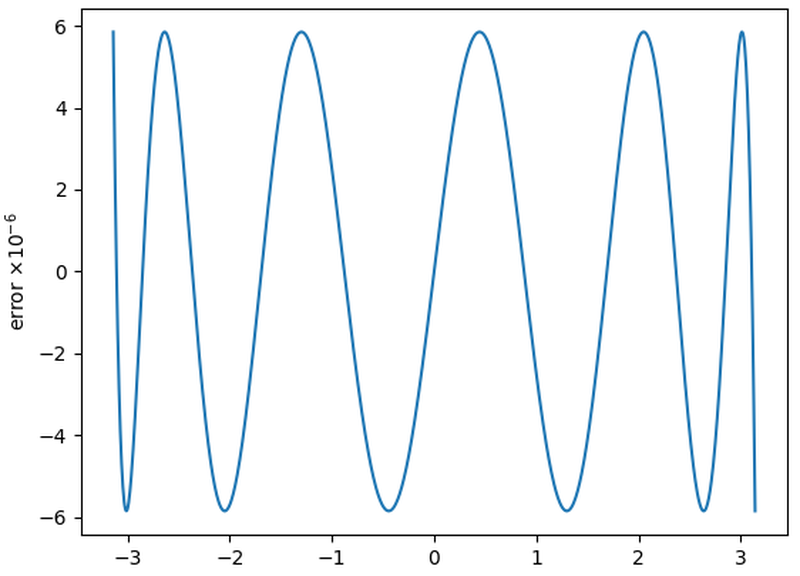
    The graph below shows the error for this polynomial. Note that the error oscillates between an upper bound and a lower bound. This is the typical appearance of a Remez polynomial. In contrast, a Taylor series will have almost no error in the middle and shoot up at the edges. This Remez polynomial was optimized for the range [-π,π]; the error explodes outside that range. The key point is that the Remez polynomial distributes the error inside the range. This minimizes the maximum error (minimax).

    Error from a Remez-optimized polynomial for sine.

    Error from a Remez-optimized polynomial for sine.
  9. I think the arctan argument is range-reduced to the range [-1/64, 1/64]. This can be accomplished with the trig identity arctan(x) = arctan((x-c)/(1+xc)) + arctan(c). The idea is that c is selected to be the value of the form n/32 closest to x. As a result, x-c will be in the desired range and the first arctan can be computed with the polynomial. The other term, arctan(c), is obtained from the lookup table in the ROM. The FPATAN (partial arctangent) instruction takes two arguments, x and y, and returns atan(y/x); this simplifies handling planar coordinates. In this case, the trig identity becomes arcan(y/x) = arctan((y-tx)/(x+ty)) + arctan c. The division operation can trigger the FDIV bug in some cases; see Computational Aspects of the Pentium Affair

  10. The Pentium has several trig instructions: FSIN, FCOS, and FSINCOS return the sine, cosine, or both (which is almost as fast as computing either). FPTAN returns the "partial tangent" consisting of two numbers that must be divided to yield the tangent. (This was due to limitations in the original 8087 coprocessor.) The Pentium returns the tangent as the first number and the constant 1 as the second number, keeping the semantics of FPTAN while being more convenient.

    The range reduction is probably based on the trig identity sin(a+b) = sin(a)cos(b)+cos(a)sin(b). To compute sin(x), select b as the closest constant in the lookup table, n/64, and then generate a=x-b. The value a will be range-reduced, so sin(a) can be computed from the polynomial. The terms sin(b) and cos(b) are available from the lookup table. The desired value sin(x) can then be computed with multiplications and addition by using the trig identity. Cosine can be computed similarly. Note that cos(a+b) =cos(a)cos(b)-sin(a)sin(b); the terms on the right are the same as for sin(a+b), just combined differently. Thus, once the terms on the right have been computed, they can be combined to generate sine, cosine, or both. The Pentium computes the tangent by dividing the sine by the cosine. This can trigger the FDIV division bug; see Computational Aspects of the Pentium Affair.

    Also see Agner Fog's Instruction Timings; the timings for the various operations give clues as to how they are computed. For instance, FPTAN takes longer than FSINCOS because the tangent is generated by dividing the sine by the cosine. 

  11. For exponentials, the F2XM1 instruction computes 2x-1; subtracting 1 improves accuracy. Specifically, 2x is close to 1 for the common case when x is close to 0, so subtracting 1 as a separate operation causes you to lose most of the bits of accuracy due to cancellation. On the other hand, if you want 2x, explicitly adding 1 doesn't harm accuracy. This is an example of how the floating-point instructions are carefully designed to preserve accuracy. For details, see the book The 8087 Primer by the architects of the 8086 processor and the 8087 coprocessor. 

  12. The Pentium has base-two logarithm instructions FYL2X and FYL2XP1. The FYL2X instruction computes y log2(x) and the FYL2XP1 instruction computes y log2(x+1) The instructions include a multiplication because most logarithm operations will need to multiply to change the base; performing the multiply with internal precision increases the accuracy. The "plus-one" instruction improves accuracy for arguments close to 1, such as interest calculations.

    My hypothesis for range reduction is that the input argument is scaled to fall between 1 and 2. (Taking the log of the exponent part of the argument is trivial since the base-2 log of a base-2 power is simply the exponent.) The argument can then be divided by the largest constant 1+n/64 less than the argument. This will reduce the argument to the range [1, 1+1/32]. The log polynomial can be evaluated on the reduced argument. Finally, the ROM constant for log2(1+n/64) is added to counteract the division. The constant is split into two parts for greater accuracy.

    It took me a long time to figure out the log constants because they were split. The upper-part constants appeared to be pointlessly inaccurate since the bottom 27 bits are zeroed out. The lower-part constants appeared to be miniscule semi-random numbers around ±10-13. Eventually, I figured out that the trick was to combine the constants. 

A surprising IC in a LED light chain.

By: cpldcpu

LED-based festive decorations are a fascinating subject for exploration of ingenuity in low-cost electronics. New products appear every year and often very surprising technology approaches are used to achieve some differentiation while adding minimal cost.

This year, there wasn’t any fancy new controller, but I was surprised how much the cost of simple light strings was reduced. The LED string above includes a small box with batteries and came in a set of ten for less than $2 shipped, so <$0.20 each. While I may have benefitted from promotional pricing, it is also clear that quite some work went into making the product cheap.

The string is constructed in the same way as one I had analyzed earlier: it uses phosphor-converted blue LEDs that are soldered to two insulated wires and covered with an epoxy blob. In contrast to the earlier device, they seem to have switched from copper wire to cheaper steel wires.

The interesting part is in the control box. It comes with three button cells, a small PCB, and a tactile button that turns the string on and cycles through different modes of flashing and and constant light.

Curiously, there is nothing on the PCB except the button and a device that looks like an LED. Also, note how some “redundant” joints have simply been left unsoldered.

Closer inspection reveals that the “LED” is actually a very small integrated circuit packaged in an LED package. The four pins are connected to the push button, the cathode of the LED string, and the power supply pins. I didn’t measure the die size exactly, but I estimate that it is smaller than 0.3×0.2 mm² = ~0.1 mm².

What is the purpose of packaging an IC in an LED package? Most likely, the company that made the light string is also packaging their own LEDs, and they saved costs by also packaging the IC themselves—in a package type they had available.

I characterized the current-voltage behavior of IC supply pins with the LED string connected. The LED string started to emit light at around 2.7V, which is consistent with the forward voltage of blue LEDs. The current increased proportionally to the voltage, which suggests that there is no current limit or constant current sink in the IC – it’s simply a switch with some series resistance.

Left: LED string in “constantly on” mode. Right: Flashing

Using an oscilloscope, I found that the string is modulated with an on-off ratio of 3:1 at a frequency if ~1.2 kHz. The image above shows the voltage at the cathode, the anode is connected to the positive supply. This is most likely to limit the current.

All in all, it is rather surprising to see an ASIC being used when it barely does more than flashing the LED string. It would have been nice to see a constant current source to stabilize the light levels over the lifetime of the battery and maybe more interesting light effects. But I guess that would have increased the cost of the ASIC too much and then using an ultra-low cost microcontroller may have been cheaper. This almost calls for a transplant of a MCU into this device…

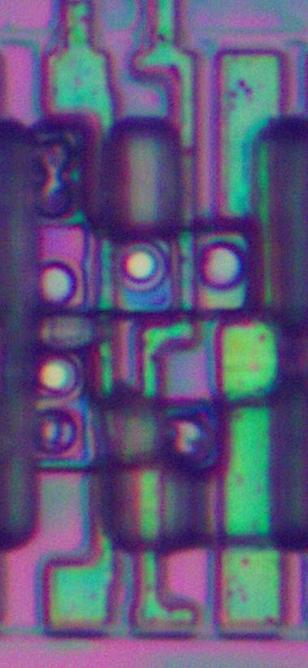
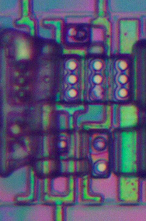
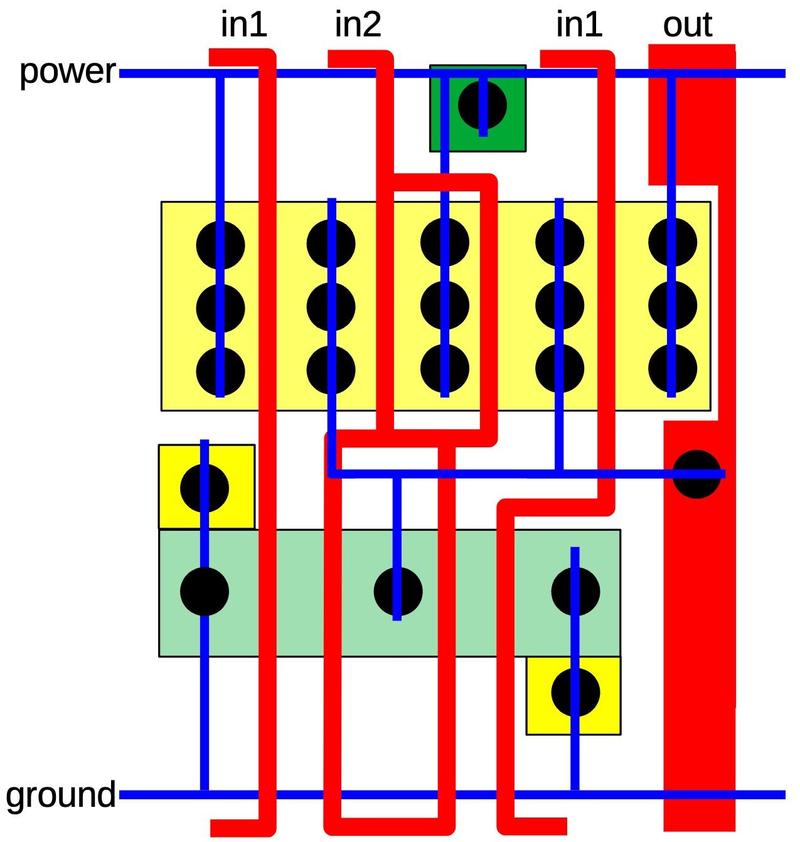
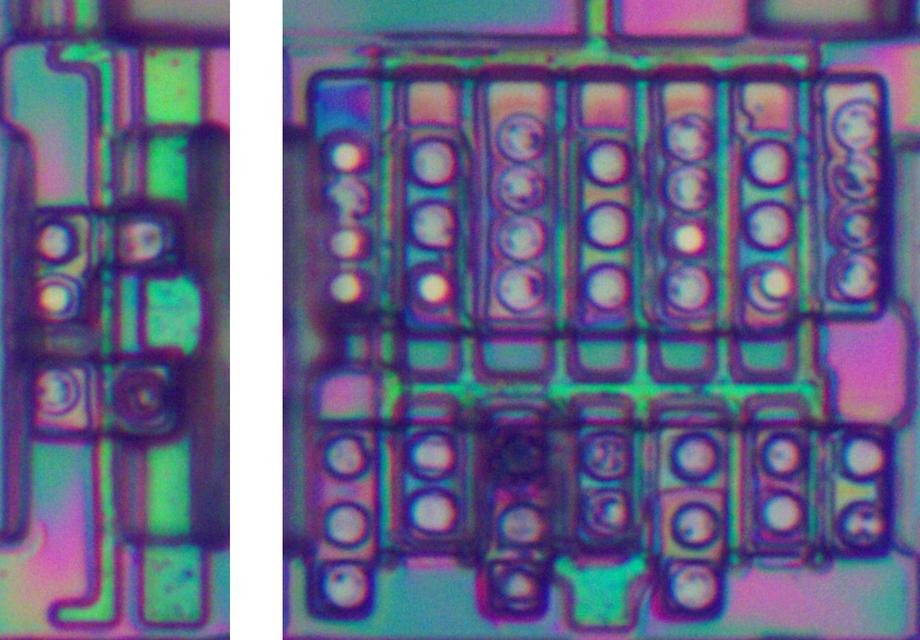
Antenna diodes in the Pentium processor

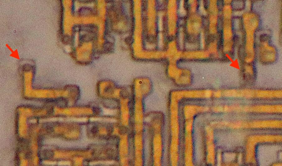
I was studying the silicon die of the Pentium processor and noticed some puzzling structures where signal lines were connected to the silicon substrate for no apparent reason. Two examples are in the photo below, where the metal wiring (orange) connects to small square regions of doped silicon (gray), isolated from the rest of the circuitry. I did some investigation and learned that these structures are "antenna diodes," special diodes that protect the circuitry from damage during manufacturing. In this blog post, I discuss the construction of the Pentium and explain how these antenna diodes work.

Closeup of the Pentium die showing the silicon and bottom metal layer. The arrows indicate connections to two antenna diodes. I removed the top two layers of metal for this photo.

Closeup of the Pentium die showing the silicon and bottom metal layer. The arrows indicate connections to two antenna diodes. I removed the top two layers of metal for this photo.

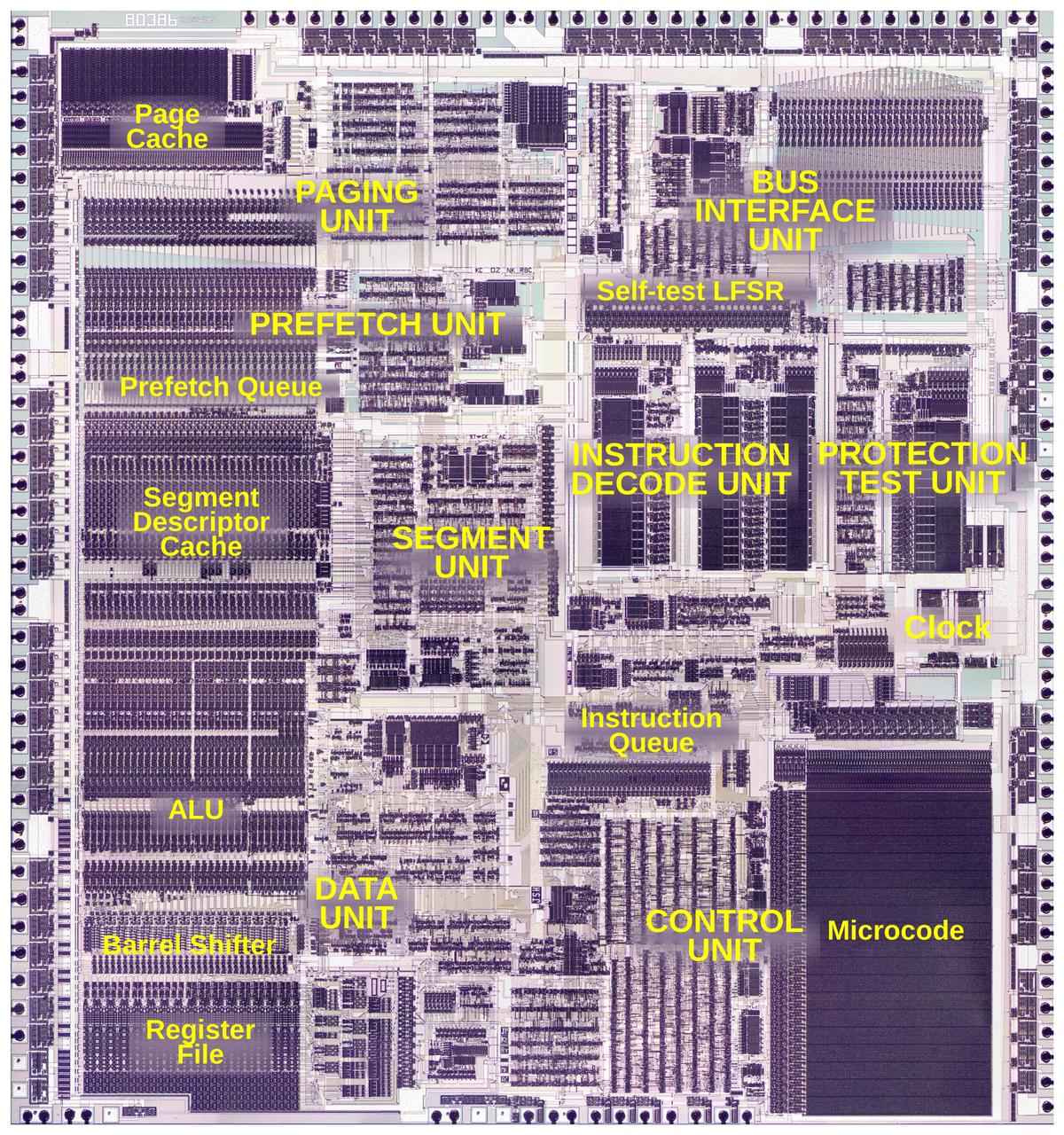
Intel released the Pentium processor in 1993, starting a long-running brand of high-performance processors: the Pentium Pro, Pentium II, and so on. In this post, I'm studying the original Pentium, which has 3.1 million transistors.1 The die photo below shows the Pentium's fingernail-sized silicon die under a microscope. The chip has three layers of metal wiring on top of the silicon so the underlying silicon is almost entirely obscured.

The Pentium die with the main functional blocks labeled. Click this photo (or any other) for a larger version.

The Pentium die with the main functional blocks labeled. Click this photo (or any other) for a larger version.

Modern processors are built from CMOS circuitry, which uses two types of transistors: NMOS and PMOS. The diagram below shows how an NMOS transistor is constructed. A transistor can be considered a switch between the source and drain, controlled by the gate. The source and drain regions (green) consist of silicon doped with impurities to change its semiconductor properties, forming N+ silicon. The gate consists of a layer of polysilicon (red), separated from the silicon by an absurdly thin insulating oxide layer. Since the oxide layer is just a few hundred atoms thick,2 it is very fragile and easily damaged by excess voltage. (This is why CMOS chips are sensitive to static electricity.) As we will see, the oxide layer can also be damaged by voltage during manufacturing.

Diagram showing the structure of an NMOS transistor.

Diagram showing the structure of an NMOS transistor.

The Pentium processor is constructed from multiple layers. Starting at the bottom, the Pentium has millions of transistors similar to the diagram above. Polysilicon wiring on top of the silicon not only forms the transistor gates but also provides short-range wiring. Above that, three layers of metal wiring connect the parts of the chip. Roughly speaking, the bottom layer of metal connects to the silicon and polysilicon to construct logic gates from the transistors, while the upper layers of wiring travel longer distances, with one layer for signals traveling horizontally and the other layer for signals traveling vertically. Tiny tungsten plugs called vias provide connections between the different layers of wiring. A key challenge of chip design is routing, directing signals through the multiple layers of wiring while packing the circuitry as densely as possible.

The photo below shows a small region of the Pentium die with the three metal layers visible. The golden vertical lines are the top metal layer, formed from aluminum and copper. Underneath, you can see the horizontal wiring of the middle metal layer. The more complex wiring of the bottom metal layer can be seen, along with the silicon and polysilicon that form transistors. The small black dots are the tungsten vias that connect metal layers, while the larger dark circles are contacts with the underlying silicon or polysilicon. Near the bottom of the photo, the vertical gray bands are polysilicon lines, forming transistor gates. Although the chip appears flat, it has a three-dimensional structure with multiple layers of metal separated by insulating layers of silicon dioxide. This three-dimensional structure will be important in the discussion below. (The metal wiring is much denser over most of the chip; this region is one of the rare spots where all the layers are visible.)

Closeup of the Pentium die showing the metal layers.
The L-shaped hook towards the lower left is a connection to an antenna diode.
This photo shows a tiny part of the floating point unit. To show all the layers in focus, I combined multiple images with focus stacking.

Closeup of the Pentium die showing the metal layers. The L-shaped hook towards the lower left is a connection to an antenna diode. This photo shows a tiny part of the floating point unit. To show all the layers in focus, I combined multiple images with focus stacking.

The manufacturing process for an integrated circuit is extraordinarily complicated but I'll skip over most of the details and focus on how each metal layer is constructed, layer by layer. First, a uniform metal layer is constructed over the silicon wafer. Next, the desired pattern is produced on the surface using a process called photolithography: a light-sensitive chemical called "resist" is applied to the wafer and exposed to light through a patterned mask. The light hardens the resist, creating a protective coating with the pattern of the desired wiring. Finally, the unprotected metal is etched away, leaving the wiring.

In the early days of integrated circuits, the metal was removed with liquid acids, a process called wet etching. Inconveniently, wet etching tended to eat away metal underneath the edges of the mask, which became a problem as integrated circuits became denser and the wires needed to be thinner. The solution was dry etch, using a plasma to remove the metal. By applying a large voltage to plates above and below the chip, a gas such as HCl is ionized into a highly reactive plasma. This plasma attacks the surface (unless it is protected by the resist), removing the unwanted metal. The advantage of dry etching is that it can act vertically (anisotropically), providing more control over the line width.

Although plasma etching improved the etching process, it caused another problem: plasma-induced oxide damage, also called (metaphorically) the "antenna effect."3 The problem is that long metal wires on the chip could pick up an electrical charge from the plasma, producing a large voltage. As described earlier, the thin oxide layer under a transistor's gate is sensitive to voltage damage. The voltage induced by the plasma can destroy the transistor by blowing a hole through the gate oxide or it can degrade the transistor's performance by embedding charges inside the oxide layer.4

Several factors affect the risk of damage from the antenna effect. First, only the transistor's gate is sensitive to the induced voltage, due to the oxide layer. If the wire is also connected to a transistor's source or drain, the wire is "safe" since the source and drain provide connections to the chip's substrate, allowing the charge to dissipate harmlessly. Note that when the chip is completed, every transistor gate is connected to another transistor's source or drain (which provides the signal to the gate), so there is no risk of damage. Thus, the problem can only occur during manufacturing, with a metal line that is connected to a gate on one end but isn't connected on the other end. Moreover, the highest layer of metal is "safe" since everything is connected at that point. Another factor is that the induced voltage is proportional to the length of the metal wire, so short wires don't pose a risk. Finally, only the metal layer currently being etched poses a risk; since the lower layers are insulated by the thick oxide between layers, they won't pick up charge.

These factors motivate several ways to prevent antenna problems.5 First, a long wire can be broken into shorter segments, connected by jumpers on a higher layer. Second, moving long wires to the top metal layer eliminates problems.6 Third, diodes can be added to drain the charge from the wire; these are called "antenna diodes". When the chip is in use, the antenna diodes are reverse-biased so they have no electrical effect. But during manufacturing, the antenna diodes let charge flow to the substrate before it causes problems.

The third solution, the antenna diodes, explains the mysterious connections that I saw in the Pentium. In the diagram below, these diodes are visible on the die as square regions of doped silicon. The larger regions of doped silicon form PMOS transistors (upper) and NMOS transistors (lower). The polysilicon lines are faintly visible; they form transistor gates where they cross the doped silicon. (For this photo, I removed all the metal wiring.)

Closeup of the Pentium die showing transistors. The metal and polysilicon layers have been removed to show the silicon.

Closeup of the Pentium die showing transistors. The metal and polysilicon layers have been removed to show the silicon.

Confusingly, the antenna diodes look almost identical to "well taps", connections from the substrate to the chip's positive voltage supply, but have a completely different purpose. In the Pentium, the PMOS transistors are constructed in "wells" of N-type silicon. These wells must be raised to the chip's positive voltage, so there are numerous well tap connections from the positive supply to the wells. The well taps consist of squares of N+ doped silicon in the the N-type silicon well, providing an electrical connection. On the other hand, the antenna diodes also consist of N+ doped silicon, but embedded in P-type silicon. This forms a P-N junction that creates the diode.

In the Pentium, antenna diodes are used for only a small fraction of the wiring. The diodes require extra area on the die, so they are used only when necessary. Most of the antenna problems on the Pentium were apparently resolved through routing. Although the antenna diodes are relatively rare, they are still frequent enough that they caught my attention.

Antenna effects are still an issue in modern integrated circuits. Integrated circuit fabricators provide rules on the maximum allowable size of antenna wires for a particular manufacturing process.7 Software checks the design to ensure that the antenna rules are not violated, modifying the routing and inserting diodes as necessary. Violating the antenna rules can result in damaged chips and a very low yield, so it's more than just a theoretical issue.

Thanks to /r/chipdesign and Discord for discussion. If you're interested in the Pentium, I've written about standard cells in the Pentium, and the Pentium as a Navajo rug. Follow me on Mastodon (@kenshirriff@oldbytes.space) or Bluesky (@righto.com) or RSS for updates.

Notes and references

  1. In this post, I'm looking at the Pentium model 80501 (codenamed P5). This model was soon replaced with a faster, lower-power version called the 80502 (P54C). Both are considered original Pentiums. 

  2. IC manufacturing drives CPU performance states that gate oxide thickness was 100 to 300 angstroms in 1993. 

  3. The wires are acting metaphorically as antennas, not literally, as they collect charge, not picking up radio waves.

    Plasma-induced oxide damage gave rise to research and conferences in the 1990s to address this problem. The International Symposium on Plasma- and Process-Induced Damage started in 1996 and continued until 2003. Numerous researchers from semiconductor companies and academia studied the causes and effects of plasma damage. 

  4. The damage is caused by "Fowler-Nordheim tunneling", where electrons tunnel through the oxide and cause damage. Flash memory uses this tunneling to erase the memory; the cumulative damage is why flash memory can only be written a limited number of times. 

  5. Some relevant papers: Magnetron etching of polysilicon: Electrical damage (1991), Thin-oxide damage from gate charging during plasma processing (1992), Antenna protection strategy for ultra-thin gate MOSFETs (1998), Fixing antenna problem by dynamic diode dropping and jumper insertion (2000). The Pentium uses the "dynamic diode dropping" approach, adding antenna diodes only as needed, rather than putting them in every circuit. I noticed that the Pentium uses extension wires to put the diode in a more distant site if there is no room for the diode under the existing wiring. As an aside, the third paper uses the curious length unit of kµm; by calling 1000 µm a kµm, you can think in micrometers, even though this unit is normally called a mm. 

  6. Sources say that routing signals on the top metal prevents antenna violations. However, I see several antenna diodes in the Pentium that are connected directly from the bottom metal (M1) through M2 to long lines on M3. These diodes seem redundant since the source/drain connections are in place by that time. So there are still a few mysteries... 

  7. Foundries have antenna rules provided as part of the Process Design Kit (PDK). Here are the rules for MOSIS and SkyWater. I've focused on antenna effects from the metal wiring, but polysilicon and vias can also cause antenna damage. Thus, there are rules for these layers too. Polysilicon wiring is less likely to cause antenna problems, though, as it is usually restricted to short distances due to its higher resistance. 

Reverse-engineering a three-axis attitude indicator from the F-4 fighter plane

We recently received an attitude indicator for the F-4 fighter plane, an instrument that uses a rotating ball to show the aircraft's orientation and direction. In a normal aircraft, the artificial horizon shows the orientation in two axes (pitch and roll), but the F-4 indicator uses a rotating ball to show the orientation in three axes, adding azimuth (yaw).1 It wasn't obvious to me how the ball could rotate in three axes: how could it turn in every direction and still remain attached to the instrument?

The attitude indicator. The "W" forms a stylized aircraft. In this case, it indicates that the aircraft is climbing slightly. Photo from CuriousMarc.

The attitude indicator. The "W" forms a stylized aircraft. In this case, it indicates that the aircraft is climbing slightly. Photo from CuriousMarc.

We disassembled the indicator, reverse-engineered its 1960s-era circuitry, fixed some problems,2 and got it spinning. The video clip below shows the indicator rotating around three axes. In this blog post, I discuss the mechanical and electrical construction of this indicator. (The quick explanation is that the ball is really two hollow half-shells attached to the internal mechanism at the "poles"; the shells rotate while the "equator" remains stationary.)

The F-4 aircraft

The indicator was used in the F-4 Phantom II3 so the pilot could keep track of the aircraft's orientation during high-speed maneuvers. The F-4 was a supersonic fighter manufactured from 1958 to 1981. Over 5000 were produced, making it the most-produced American supersonic aircraft ever. It was the main US fighter jet in the Vietnam War, operating from aircraft carriers. The F-4 was still used in the 1990s during the Gulf War, suppressing air defenses in the "Wild Weasel" role. The F-4 was capable of carrying nuclear bombs.4

An F-4G Phantom II Wild Weasel aircraft. From National Archives.

An F-4G Phantom II Wild Weasel aircraft. From National Archives.

The F-4 was a two-seat aircraft, with the radar intercept officer controlling radar and weapons from a seat behind the pilot. Both cockpits had a panel crammed with instruments, with additional instruments and controls on the sides. As shown below, the pilot's panel had the three-axis attitude indicator in the central position, just below the reddish radar scope, reflecting its importance.5 (The rear cockpit had a simpler two-axis attitude indicator.)

The cockpit of the F-4C Phantom II, with the attitude indicator in the center of the panel. Click this photo (or any other) for a larger version. Photo from National Museum of the USAF.

The cockpit of the F-4C Phantom II, with the attitude indicator in the center of the panel. Click this photo (or any other) for a larger version. Photo from National Museum of the USAF.

The attitude indicator mechanism

The ball inside the indicator shows the aircraft's position in three axes. The roll axis indicates the aircraft's angle if it rolls side-to-side along its axis of flight. The pitch axis indicates the aircraft's angle if it pitches up or down. Finally, the azimuth axis indicates the compass direction that the aircraft is heading, changed by the aircraft's turning left or right (yaw). The indicator also has moving needles and status flags, but in this post I'm focusing on the rotating ball.6

The indicator uses three motors to move the ball. The roll motor (below) is attached to the frame of the indicator, while the pitch and azimuth motors are inside the ball. The ball is held in place by the roll gimbal, which is attached to the ball mechanism at the top and bottom pivot points. The roll motor turns the roll gimbal and thus the ball, providing a clockwise/counterclockwise movement. The roll control transformer provides position feedback. Note the numerous wires on the roll gimbal, connected to the mechanism inside the ball.

The attitude indicator with the cover removed.

The attitude indicator with the cover removed.

The diagram below shows the mechanism inside the ball, after removing the hemispherical shells of the ball. When the roll gimbal is rotated, this mechanism rotates with it. The pitch motor causes the entire mechanism to rotate around the pitch axis (horizontal here), which is attached along the "equator". The azimuth motor and control transformer are behind the pitch components, not visible in this photo. The azimuth motor turns the vertical shaft. The two hollow hemispheres of the ball attach to the top and bottom of the shaft. Thus, the azimuth motor rotates the ball shells around the azimuth axis, while the mechanism itself remains stationary.

The components of the ball mechanism.

The components of the ball mechanism.

Why doesn't the wiring get tangled up as the ball rotates? The solution is two sets of slip rings to implement the electrical connections. The photo below shows the first slip ring assembly, which handles rotation around the roll axis. These slip rings connect the stationary part of the instrument to the rotating roll gimbal. The black base and the vertical wires are attached to the instrument, while the striped shaft in the middle rotates with the ball assembly housing. Inside the shaft, wires go from the circular metal contacts to the roll gimbal.

The first set of slip rings. Yes, there is damage on one of the slip ring contacts.

The first set of slip rings. Yes, there is damage on one of the slip ring contacts.

Inside the ball, a second set of slip rings provides the electrical connection between the wiring on the roll gimbal and the ball mechanism. The photo below shows the connections to these slip rings, handling rotation around the pitch axis (horizontal in this photo). (The slip rings themselves are inside and are not visible.) The shaft sticking out of the assembly rotates around the azimuth (yaw) axis. The ball hemisphere is attached to the metal disk. The azimuth axis does not require slip rings since only the ball shells rotates; the electronics remain stationary.

Connections for the second set of slip rings.

Connections for the second set of slip rings.

The servo loop

In this section, I'll explain how the motors are controlled by servo loops. The attitude indicator is driven by an external gyroscope, receiving electrical signals indicating the roll, pitch, and azimuth positions. As was common in 1960s avionics, the signals are transmitted from synchros, which use three wires to indicate an angle. The motors inside the attitude indicator rotate until the indicator's angles for the three axes match the input angles.

Each motor is controlled by a servo loop, shown below. The goal is to rotate the output shaft to an angle that exactly matches the input angle, specified by the three synchro wires. The key is a device called a control transformer, which takes the three-wire input angle and a physical shaft rotation, and generates an error signal indicating the difference between the desired angle and the physical angle. The amplifier drives the motor in the appropriate direction until the error signal drops to zero. To improve the dynamic response of the servo loop, the tachometer signal is used as a negative feedback voltage. This ensures that the motor slows as the system gets closer to the right position, so the motor doesn't overshoot the position and oscillate. (This is sort of like a PID controller.)

This diagram shows the structure of the servo loop, with a feedback loop ensuring that the rotation angle of the output shaft matches the input angle.

This diagram shows the structure of the servo loop, with a feedback loop ensuring that the rotation angle of the output shaft matches the input angle.

In more detail, the external gyroscope unit contains synchro transmitters, small devices that convert the angular position of a shaft into AC signals on three wires. The photo below shows a typical synchro, with the input shaft on the top and five wires at the bottom: two for power and three for the output.

A synchro transmitter.

A synchro transmitter.

Internally, the synchro has a rotating winding called the rotor that is driven with 400 Hz AC. Three fixed stator windings provide the three AC output signals. As the shaft rotates, the phase and voltage of the output signals changes, indicating the angle. (Synchros may seem bizarre, but they were extensively used in the 1950s and 1960s to transmit angular information in ships and aircraft.)

The schematic symbol for a synchro transmitter or receiver.

The schematic symbol for a synchro transmitter or receiver.

The attitude indicator uses control transformers to process these input signals. A control transformer is similar to a synchro in appearance and construction, but it is wired differently. The three stator windings receive the inputs and the rotor winding provides the error output. If the rotor angle of the synchro transmitter and control transformer are the same, the signals cancel out and there is no error output. But as the difference between the two shaft angles increases, the rotor winding produces an error signal. The phase of the error signal indicates the direction of error.

The next component is the motor/tachometer, a special motor that was often used in avionics servo loops. This motor is more complicated than a regular electric motor. The motor is powered by 115 volts AC, 400-Hertz, but this isn't sufficient to get the motor spinning. The motor also has two low-voltage AC control windings. Energizing a control winding will cause the motor to spin in one direction or the other.

The motor/tachometer unit also contains a tachometer to measure its rotational speed, for use in a feedback loop. The tachometer is driven by another 115-volt AC winding and generates a low-voltage AC signal proportional to the rotational speed of the motor.

A motor/tachometer similar (but not identical) to the one in the attitude indicator).

A motor/tachometer similar (but not identical) to the one in the attitude indicator).

The photo above shows a motor/tachometer with the rotor removed. The unit has many wires because of its multiple windings. The rotor has two drums. The drum on the left, with the spiral stripes, is for the motor. This drum is a "squirrel-cage rotor", which spins due to induced currents. (There are no electrical connections to the rotor; the drums interact with the windings through magnetic fields.) The drum on the right is the tachometer rotor; it induces a signal in the output winding proportional to the speed due to eddy currents. The tachometer signal is at 400 Hz like the driving signal, either in phase or 180º out of phase, depending on the direction of rotation. For more information on how a motor/generator works, see my teardown.

The amplifier

The motors are powered by an amplifier assembly that contains three separate error amplifiers, one for each axis. I had to reverse engineer the amplifier assembly in order to get the indicator working. The assembly mounts on the back of the attitude indicator and connects to one of the indicator's round connectors. Note the cutout in the lower left of the amplifier assembly to provide access to the second connector on the back of the indicator. The aircraft connects to the indicator through the second connector and the indicator passes the input signals to the amplifier through the connector shown above.

The amplifier assembly.

The amplifier assembly.

The amplifier assembly contains three amplifier boards (for roll, pitch, and azimuth), a DC power supply board, an AC transformer, and a trim potentiometer.7 The photo below shows the amplifier assembly mounted on the back of the instrument. At the left, the AC transformer produces the motor control voltage and powers the power supply board, mounted vertically on the right. The assembly has three identical amplifier boards; the middle board has been unmounted to show the components. The amplifier connects to the instrument through a round connector below the transformer. The round connector at the upper left is on the instrument case (not the amplifier) and provides the connection between the aircraft and the instrument.8

The amplifier assembly mounted on the back of the instrument. We are feeding test signals to the connector in the upper left.

The amplifier assembly mounted on the back of the instrument. We are feeding test signals to the connector in the upper left.

The photo below shows one of the three amplifier boards. The construction is unusual, with some components stacked on top of other components to save space. Some of the component leads are long and protected with clear plastic sleeves. The board is connected to the rest of the amplifier assembly through a bundle of point-to-point wires, visible on the left. The round pulse transformer in the middle has five colorful wires coming out of it. At the right are the two transistors that drive the motor's control windings, with two capacitors between them. The transistors are mounted on a heat sink that is screwed down to the case of the amplifier assembly for cooling. The board is covered with a conformal coating to protect it from moisture or contaminants.

One of the three amplifier boards.

One of the three amplifier boards.

The function of each amplifier board is to generate the two control signals so the motor rotates in the appropriate direction based on the error signal fed into the amplifier. The amplifier also uses the tachometer output from the motor unit to slow the motor as the error signal decreases, preventing overshoot. The inputs to the amplifier are 400 hertz AC signals, with the phase indicating positive or negative error. The outputs drive the two control windings of the motor, determining which direction the motor rotates.

The schematic for the amplifier board is below. The two transistors on the left amplify the error and tachometer signals, driving the pulse transformer. The outputs of the pulse transformer will have opposite phase, driving the output transistors for opposite halves of the 400 Hz cycle. One of the transistors will be in the right phase to turn on and pull the motor control AC to ground, while the other transistor will be in the wrong phase. Thus, the appropriate control winding will be activated (for half the cycle), causing the motor to spin in the desired direction.

Schematic of one of the three amplifier boards. (Click for a larger version.)

Schematic of one of the three amplifier boards. (Click for a larger version.)

It turns out that there are two versions of the attitude indicator that use incompatible amplifiers. I think that the motors for the newer indicators have a single control winding rather than two. Fortunately, the connectors are keyed differently so you can't attach the wrong amplifier. The second amplifier (below) looks slightly more modern (1980s) with a double-sided circuit board and more components in place of the pulse transformer.

The second type of amplifier board.

The second type of amplifier board.

The pitch trim circuit

The attitude indicator has a pitch trim knob in the lower right, although the knob was missing from ours. The pitch trim adjustment turns out to be rather complicated. In level flight, an aircraft may have its nose angled up or down slightly to achieve the desired angle of attack. The pilot wants the attitude indicator to show level flight, even though the aircraft is slightly angled, so the indicator can be adjusted with the pitch trim knob. However, the problem is that a fighter plane may, for instance, do a vertical 90º climb. In this case, the attitude indicator should show the actual attitude and ignore the pitch trim adjustment.

I found a 1957 patent that explained how this is implemented. The solution is to "fade out" the trim adjustment when the aircraft moves away from horizontal flight. This is implemented with a special multi-zone potentiometer that is controlled by the pitch angle.

The schematic below shows how the pitch trim signal is generated from the special pitch angle potentiometer and the pilot's pitch trim adjustment. Like most signals in the attitude indicator, the pitch trim is a 400 Hz AC signal, with the phase indicating positive or negative. Ignoring the pitch angle for a moment, the drive signal into the transformer will be AC. The split windings of the transformer will generate a positive phase and a negative phase signal. Adjusting the pitch trim potentiometer lets the pilot vary the trim signal from positive to zero to negative, applying the desired correction to the indicator.

The pitch trim circuit. Based on the patent.

The pitch trim circuit. Based on the patent.

Now, look at the complex pitch angle potentiometer. It has alternating resistive and conducting segments, with AC fed into opposite sides. (Note that +AC and -AC refer to the phase, not the voltage.) Because the resistances are equal, the AC signals will cancel out at the top and the bottom, yielding 0 volts on those segments. If the aircraft is roughly horizontal, the potentiometer wiper will pick up the positive-phase AC and feed it into the transformer, providing the desired trim adjustment as described previously. However, if the aircraft is climbing nearly vertically, the wiper will pick up the 0-volt signal, so there will be no pitch trim adjustment. For an angle range in between, the resistance of the potentiometer will cause the pitch trim signal to smoothly fade out. Likewise, if the aircraft is steeply diving, the wiper will pick up the 0 signal at the bottom, removing the pitch trim. And if the aircraft is inverted, the wiper will pick up the negative AC phase, causing the pitch trim adjustment to be applied in the opposite direction.

Conclusions

The attitude indicator is a key instrument in any aircraft, especially important when flying in low visibility. The F-4's attitude indicator goes beyond the artificial horizon indicator in a typical aircraft, adding a third axis to show the aircraft's heading. Supporting a third axis makes the instrument much more complicated, though. Looking inside the indicator reveals how the ball rotates in three axes while still remaining firmly attached.

Modern fighter planes avoid complex electromechanical instruments. Instead, they provide a "glass cockpit" with most data provided digitally on screens. For instance, the F-35's console replaces all the instruments with a wide panoramic touchscreen displaying the desired information in color. Nonetheless, mechanical instruments have a special charm, despite their impracticality.

For more, follow me on Mastodon as @kenshirriff@oldbytes.space or RSS. (I've given up on Twitter.) I worked on this project with CuriousMarc and Eric Schlapfer, so expect a video at some point. Thanks to John Pumpkinhead and another collector for supplying the indicators and amplifiers.

Notes and references

Specifications9

  1. This three-axis attitude indicator is similar in many ways to the FDAI (Flight Director Attitude Indicator) that was used in the Apollo space flights, although the FDAI has more indicators and needles. It is more complex than the Soyus Globus, used for navigation (teardown), which rotates in two axes. Maybe someone will loan us an FDAI to examine...
     

  2. Our indicator has been used as a parts source, as it has cut wires inside and is missing the pitch trim knob, several needles, and internal adjustment potentiometers. We had to replace two failed capacitors in the power supply. There is still a short somewhere that we are tracking down; at one point it caused the bond wire inside a transistor to melt(!). 

  3. The aircraft is the "Phantom II" because the original Phantom was a World War II fighter aircraft, the McDonnell FH Phantom. McDonnell Douglas reused the Phantom name for the F-4. (McDonnell became McDonnell Douglas in 1967 after merging with Douglas Aircraft. McDonnell Douglas merged into Boeing in 1997. Many people blame Boeing's current problems on this merger.) 

  4. The F-4 could carry a variety of nuclear bombs such as the B28EX, B61, B43 and B57, referred to as "special weapons". The photo below shows the nuclear store consent switch, which armed a nuclear bomb for release. (Somehow I expected a more elaborate mechanism for nuclear bombs.) The switch labels are in the shadows, but say "REL/ARM", "SAFE", and "REL". The F-4 Weapons Delivery Manual discusses this switch briefly.

    The nuclear store consent switch, to the right of the Weapons System Officer in the rear cockpit. Photo from National Museum of the USAF.

    The nuclear store consent switch, to the right of the Weapons System Officer in the rear cockpit. Photo from National Museum of the USAF.


  5. The photo below is a closeup of the attitude indicator in the F-4 cockpit. Note the Primary/Standby toggle switch in the upper-left. Curiously, this switch is just screwed onto the console, with exposed wires. Based on other sources, this appears to be the standard mounting. This switch is the "reference system selector switch" that selects the data source for the indicator. In the primary setting, the gyroscopically-stabilized inertial navigation system (INS) provides the information. The INS normally gets azimuth information from the magnetic compass, but can use a directional gyro if the Earth's magnetic field is distorted, such as in polar regions. See the F-4E Flight Manual for details.

    A closeup of the indicator in the cockpit of the F-4 Phantom II. Photo from National Museum of the USAF.

    A closeup of the indicator in the cockpit of the F-4 Phantom II. Photo from National Museum of the USAF.

    The standby switch setting uses the bombing computer (the AN/AJB-7 Attitude-Reference Bombing Computer Set) as the information source; it has two independent gyroscopes. If the main attitude indicator fails entirely, the backup is the "emergency attitude reference system", a self-contained gyroscope and indicator below and to the right of the main attitude indicator; see the earlier cockpit photo. 

  6. The diagram below shows the features of the indicator.

    The features of the Attitude Director Indicator (ADI). From F-4E Flight Manual TO 1F-4E-1.

    The features of the Attitude Director Indicator (ADI). From F-4E Flight Manual TO 1F-4E-1.

    The pitch steering bar is used for an instrument (ILS) landing. The bank steering bar provides steering information from the navigation system for the desired course. 

  7. The roll, pitch, and azimuth inputs require different resistances, for instance, to handle the pitch trim input. These resistors are on the power supply board rather than an amplifier board. This allows the three amplifier boards to be identical, rather than having slightly different amplifier boards for each axis. 

  8. The attitude indicator assembly has a round mil-spec connector and the case has a pass-through connector. That is, the aircraft wiring plugs into the outside of the case and the indicator internals plug into the inside of the case. The pin numbers on the outside of the case don't match the pin numbers on the internal connector, which is very annoying when reverse-engineering the system. 

  9. In this footnote, I'll link to some of the relevant military specifications.

    The attitude indicator is specified in military spec MIL-I-27619, which covers three similar indicators, called ARU-11/A, ARU-21/A, and ARU-31/A. The three indicators are almost identical except the the ARU-21/A has the horizontal pointer alarm flag and the ARU-31/A has a bank angle command pointer and a bank scale at the bottom of the indicator, along with a bank angle command pointer adjustment knob in the lower left. The ARU-11/A was used in the F-111A. (The ID-1144/AJB-7 indicator is probably the same as the ARU-11/A.) The ARU-21/A was used in the A-7D Corsair. The ARU-31/A was used in the RF-4C Phantom II, the reconnaissance version of the F-4. The photo below shows the cockpit of the RF-4C; note that the attitude indicator in the center of the panel has two knobs.

    Cockpit panel of the RF-4C. Photo from National Museum of the USAF.

    Cockpit panel of the RF-4C. Photo from National Museum of the USAF.

    The indicator was part of the AN/ASN-55 Attitude Heading Reference Set, specified in MIL-A-38329. I think that the indicator originally received its information from an MD-1 gyroscope (MIL-G-25597) and an ML-1 flux valve compass, but I haven't tracked down all the revisions and variants.

    Spec MIL-I-23524 describes an indicator that is almost identical to the ARU-21/A but with white flags. This indicator was also used with the AJB-3A Bomb Release Computing Set, part of the A-4 Skyhawk. This indicator was used with the integrated flight information system MIL-S-23535 which contained the flight director computer MIL-S-23367.

    My indicator has no identifying markings, so I can't be sure of its exact model. Moreover, it has missing components, so it is hard to match up the features. Since my indicator has white flags it might be the ID-1329/A.


Inside a ferroelectric RAM chip

Ferroelectric memory (FRAM) is an interesting storage technique that stores bits in a special "ferroelectric" material. Ferroelectric memory is nonvolatile like flash memory, able to hold its data for decades. But, unlike flash, ferroelectric memory can write data rapidly. Moreover, FRAM is much more durable than flash and can be be written trillions of times. With these advantages, you might wonder why FRAM isn't more popular. The problem is that FRAM is much more expensive than flash, so it is only used in niche applications.

Die of the Ramtron FM24C64 FRAM chip. (Click this image (or any other) for a larger version.)

Die of the Ramtron FM24C64 FRAM chip. (Click this image (or any other) for a larger version.)

This post takes a look inside an FRAM chip from 1999, designed by a company called Ramtron. The die photo above shows this 64-kilobit chip under a microscope; the four large dark stripes are the memory cells, containing tiny cubes of ferroelectric material. The horizontal greenish bands are the drivers to select a column of memory, while the vertical greenish band at the right holds the sense amplifiers that amplify the tiny signals from the memory cells. The eight whitish squares around the border of the die are the bond pads, which are connected to the chip's eight pins.1 The logic circuitry at the left and right of the die implements the serial (I2C) interface for communication with the chip.2

The history of ferroelectric memory dates back to the early 1950s.3 Many companies worked on FRAM from the 1950s to the 1970s, including Bell Labs, IBM, RCA, and Ford. The 1955 photo below shows a 256-bit ferroelectric memory built by Bell Labs. Unfortunately, ferroelectric memory had many problems,4 limiting it to specialized applications, and development was mostly abandoned by the 1970s.

A 256-bit ferroelectric memory made by Bell Labs. Photo from Scientific American, June, 1955.

A 256-bit ferroelectric memory made by Bell Labs. Photo from Scientific American, June, 1955.

Ferroelectric memory had a second chance, though. A major proponent of ferroelectric memory was George Rohrer, who started working on ferroelectric memory in 1968. He formed a memory company, Technovation, which was unsuccessful, and then cofounded Ramtron in 1984.5 Ramtron produced a tiny 256-bit memory chip in 1988, followed by much larger memories in the 1990s.

How FRAM works

Ferroelectric memory uses a special material with the property of ferroelectricity. In a normal capacitor, applying an electric field causes the positive and negative charges to separate in the dielectric material, making it polarized. However, ferroelectric materials are special because they will retain this polarization even when the electric field is removed. By polarizing a ferroelectric material positively or negatively, a bit of data can be stored. (The name "ferroelectric" is in analogy to "ferromagnetic", even though ferroelectric materials are not ferrous.)

This FRAM chip uses a ferroelectric material called lead zirconate titanate or PZT, containing lead, zirconium, titanium, and oxygen. The diagram below shows how an applied electric field causes the titanium or zirconium atom to physically move inside the crystal lattice, causing the ferroelectric effect. (Red atoms are lead, purple are oxygen, and yellow are zirconium or titanium.) Because the atoms physically change position, the polarization is stable for decades; in contrast, the capacitors in a DRAM chip lose their data in milliseconds unless refreshed. FRAM memory will eventually wear out, but it can be written trillions of times, much more than flash or EEPROM memory.

The ferroelectric effect in the PZT crystal. From Ramtron Catalog, cleaned up.

The ferroelectric effect in the PZT crystal. From Ramtron Catalog, cleaned up.

To store data, FRAM uses ferroelectric capacitors, capacitors with a ferroelectric material as the dielectric between the plates. Applying a voltage to the capacitor will create an electric field, polarizing the ferroelectric material. A positive voltage will store a 1, and a negative voltage will store a 0.

Reading a bit from memory is a bit tricky. A positive voltage is applied, forcing the material into the 1 state. If the material was already in the 1 state, minimal current will flow. But if the material was in the 0 state, more current will flow as the capacitor changes state. This allows the 0 and 1 states to be distinguished.

Note that reading the bit destroys the stored value. Thus, after a read, the 0 or 1 value must be written back to the capacitor to restore its previous state. (This is very similar to the magnetic core memory that was used in the 1960s.)6

The FRAM chip that I examined uses two capacitors per bit, storing opposite values. This approach makes it easier to distinguish a 1 from a 0: a sense amplifier compares the two tiny signals and generates a 1 or a 0 depending on which is larger. The downside of this approach is that using two capacitors per bit reduces the memory capacity. Later FRAMs increased the density by using one capacitor per bit, along with reference cells for comparison.7

A closer look at the die

The diagram below shows the main functional blocks of the chip.8 The memory itself is partitioned into four blocks. The word line decoders select the appropriate column for the address and the drivers generate the pulses on the word and plate lines. The signals from that column go to the sense amplifiers on the right, where the signals are converted to bits and written back to memory. On the left, the precharge circuitry charges the bit lines to a fixed voltage at the start of the memory cycle, while the decoders select the desired byte from the bit lines.

The die with the main functional blocks labeled.

The die with the main functional blocks labeled.

The diagram below shows a closeup of the memory. I removed the top metal layer and many of the memory cells to reveal the underlying structure. The structure is very three-dimensional compared to regular chips; the gray squares in the image are cubes of PZT, sitting on top of the plate lines. The brown rectangles labeled "top plate connection" are also three-dimensional; they are S-shaped brackets with the low end attached to the silicon and the high end contacting the top of the PZT cube. Thus, each PZT cube forms a capacitor with the plate line forming the bottom plate of the capacitor, the bracket forming the top plate connection, and the PZT cube sandwiched in between, providing the ferroelectric dielectric. (Some cubes have been knocked loose in this photo and are sitting at an angle; the cubes form a regular grid in the original chip.)

Structure of the memory. The image is focus-stacked for clarity.

Structure of the memory. The image is focus-stacked for clarity.

The physical design of the chip is complicated and quite different from a typical planar integrated circuit. Each capacitor requires a cube of PZT sandwiched between platinum electrodes, with the three-dimensional contact from the top of the capacitor to the silicon. Creating these structures requires numerous steps that aren't used in normal integrated circuit fabrication. (See the footnote9 for details.) Moreover, the metal ions in the PZT material can contaminate the silicon production facility unless great care is taken, such as using a separate facility to apply the ferroelectric layer and all subsequent steps.10 The additional fabrication steps and unusual materials significantly increase the cost of manufacturing FRAM.

Each top plate connection has an associated transistor, gated by a vertical word line.11 The transistors are connected to horizontal bit lines, metal lines that were removed for this photo. A memory cell, containing two capacitors, measures about 4.2 µm × 6.5 µm. The PZT cubes are spaced about 2.1 µm apart. The transistor gate length is roughly 700 nm. The 700 nm node was introduced in 1993, while the die contains a 1999 copyright date, so the chip appears to be a few years behind the cutting edge as far as node.

The memory is organized as 256 capacitors horizontally by 512 capacitors vertically, for a total of 64 kilobits (since each bit requires two capacitors). The memory is accessed as 8192 bytes. Curiously, the columns are numbered on the die, as shown below.

With the metal removed, the numbers are visible counting the columns.

With the metal removed, the numbers are visible counting the columns.

The photo below shows the sense amplifiers to the right of the memory, with some large transistors to boost the signal. Each sense amplifier receives two signals from the pair of capacitors holding a bit. The sense amplifier determines which signal is larger, deciding if the bit is a 0 or 1. Because the signals are very small, the sense amplifier must be very sensitive. The amplifier has two cross-connected transistors with each transistor trying to pull the other signal low. The signal that starts off larger will "win", creating a solid 0 or 1 signal. This value is rewritten to memory to restore the value, since reading the value erases the cells. In the photo, a few of the ferroelectric capacitors are visible at the far left. Part of the lower metal layer has come loose, causing the randomly strewn brown rectangles.

The sense amplifiers.

The sense amplifiers.

The photo below shows eight of the plate drivers, below the memory cells. This circuit generates the pulse on the selected plate line. The plate lines are the thick white lines at the top of the image; they are platinum so they appear brighter in the photo than the other metal lines. Most of the capacitors are still present on the plate lines, but some capacitors have come loose and are scattered on the rest of the circuitry. Each plate line is connected to a metal line (brown), which connects the plate line to the drive transistors in the middle and bottom of the image. These transistors pull the appropriate plate line high or low as necessary. The columns of small black circles are connections between the metal line and the silicon of the transistor underneath.

The plate driver circuitry.

The plate driver circuitry.

Finally, here's the part number and Ramtron logo on the die.

Closeup of the logo "FM24C64A Ramtron" on the die.

Closeup of the logo "FM24C64A Ramtron" on the die.

Conclusions

Ferroelectric RAM is an example of a technology with many advantages that never achieved the hoped-for success. Many companies worked on FRAM from the 1950s to the 1970s but gave up on it. Ramtron tried again and produced products but they were not profitable. Ramtron had hoped that the density and cost of FRAM would be competitive with DRAM, but unfortunately that didn't pan out. Ramtron was acquired by Cypress Semiconductor in 2012 and then Cypress was acquired by Infineon in 2019. Infineon still sells FRAM, but it is a niche product, for instance satellites that need radiation hardness. Currently, FRAM costs roughly $3/megabit, almost three orders of magnitude more expensive than flash memory, which is about $15/gigabit. Nonetheless, FRAM is a fascinating technology and the structures inside the chip are very interesting.

For more, follow me on Mastodon as @kenshirriff@oldbytes.space or RSS. (I've given up on Twitter.) Thanks to CuriousMarc for providing the chip, which was used in a digital readout (DRO) for his CNC machine.

Notes and references

  1. The photo below shows the chip's 8-pin package.

    The chip is packaged in an 8-pin DIP. "RIC" stands for Ramtron International Corporation.

    The chip is packaged in an 8-pin DIP. "RIC" stands for Ramtron International Corporation.


  2. The block diagram shows the structure of the chip, which is significantly different from a standard DRAM chip. The chip has logic to handle the I2C protocol, a serial protocol that uses a clock and a data line. (Note that the address lines A0-A2 are the address of the chip, not the memory address.) The WP (Write Protect) pin, protects one quarter of the chip from being modified. The chip allows an arbitrary number of bytes to be read or written sequentially in one operation. This is implemented by the counter and address latch.

    Block diagram of the FRAM chip. From the datasheet.

    Block diagram of the FRAM chip. From the datasheet.


  3. An early description of ferroelectric memory is in the October 1953 Proceedings of the IRE. This issue focused on computers and had an article on computer memory systems by J. P. Eckert of ENIAC fame. In 1953, computer memory systems were primitive: mercury delay lines, electrostatic CRTs (Williams tubes), or rotating drums. The article describes experimental memory technologies including ferroelectric memory, magnetic core memory, neon-capacitor memory, phosphor drums, temperature-sensitive pigments, corona discharge, or electrolytic diodes. Within a couple of years, magnetic core memory became successful, dominating storage until semiconductor memory took over in the 1970s, and most of the other technologies were forgotten. 

  4. A 1969 article in Electronics discussed ferroelectric memories. At the time, ferroelectric memories were used for a few specialized applications. However, ferroelectric memories had many issues: slow write speed, high voltages (75 to 150 volts), and expensive logic to decode addresses. The article stated: "These considerations make the future of ferroelectric memories in computers rather bleak." 

  5. Interestingly, the "Ram" in Ramtron comes from the initials of the cofounders: Rohrer, Araujo, and McMillan. Rohrer originally focused on potassium nitrate as the ferroelectric material, as described in his patent. (I find it surprising that potassium nitrate is ferroelectric since it seems like such a simple, non-exotic chemical.) An extensive history of Ramtron is here. A Popular Science article also provides information. 

  6. Like core memory, ferroelectric memory is based on a hysteresis loop. Because of the hysteresis loop, the material has two stable states, storing a 0 or 1. While core memory has a hysteresis loop for magnetization with respect to the magnetic field, ferroelectric memory The difference is that core memory has hysteresis of the magnetization with respect to the applied magnetic field, while ferroelectric memory has hysteresis of the polarization with respect to the applied electric field. 

  7. The reference cell approach is described in Ramtron patent 6028783A. The idea is to have a row of reference capacitors, but the reference capacitors are sized to generate a current midway between the 0 current and the 1 current. The reference capacitors provide the second input to the sense amplifiers, allowing the 0 and 1 bits to be distinguished. 

  8. Ramtron's 1987 patent describes the approximate structure of the memory. 

  9. The diagram below shows the complex process that Ramtron used to create an FRAM chip. (These steps are from a 2003 patent, so they may differ from the steps for the chip I examined.)

    Ramtron's process flow to create an FRAM die. From Patent 6613586.

    Ramtron's process flow to create an FRAM die. From Patent 6613586.

    Abbreviations: BPSG is borophosphosilicate glass. UTEOS is undoped tetraethylorthosilicate, a liquid used to deposit silicon dioxide on the surface. RTA is rapid thermal anneal. PTEOS is phosphorus-doped tetraethylorthosilicate, used to create a phosphorus-doped silicon dioxide layer. CMP is chemical mechanical planarization, polishing the die surface to be flat. TEC is the top electrode contact. ILD is interlevel dielectric, the insulating layer between conducting layers. 

  10. See the detailed article Ferroelectric Memories, Science, 1989, by Scott and Araujo (who is the "A" in "Ramtron"). 

  11. Early FRAM memories used an X-Y grid of wires without transistors. Although much simpler, this approach had the problem that current could flow through unwanted capacitors via "sneak" paths, causing noise in the signals and potentially corrupting data. High-density integrated circuits, however, made it practical to associate a transistor with each cell in modern FRAM chips. 

Inside the guidance system and computer of the Minuteman III nuclear missile

The Minuteman missile was introduced in 1962 as a key part of America's nuclear deterrent. The Minuteman III missile is currently the only US land-based intercontinental ballistic missile (ICBM), with 400 missiles ready for launch, spread across five central states.1 The missile contains a precision guidance system, capable of delivering a warhead to a target 13,000 km away (8000 miles) with an accuracy of 200 meters (660 feet).

The diagram below shows the guidance system of the Minuteman III missile (1970). This guidance system contains over 17,000 electronic and mechanical parts, costing $510,000 (about $4.5 million in current dollars). The heart of the guidance system is the gyro stabilized platform, which uses gyroscopes and accelerometers to measure the missile's orientation and acceleration. The computer uses the measurements from the platform to determine the missile's position and guide the missile on its trajectory to the target. Other key components are the missile guidance set controller, which contains electronics to support the gyro stabilized platform, and the amplifier, which interfaces the computer with the rest of the missile. In this blog post, I take a close look at the components of the guidance system that was used until the early 2000s.2

The Minuteman III guidance system (NS-20). Click on this image (or any other) for a larger version. Original image from National Air and Space Museum.

The Minuteman III guidance system (NS-20). Click on this image (or any other) for a larger version. Original image from National Air and Space Museum.

Fundamentally, the guidance computer constantly compares the missile position to the desired trajectory and generates the appropriate steering commands to keep the missile on track.3 The diagram below shows how directing the engine nozzles causes the missile to rotate around its three axes: roll, pitch, and yaw.4 In the silo, the roll angle (the azimuth) is aligned with the direction to the target. The missile takes off vertically and then the missile gradually rotates along the pitch axis to tilt over toward the target. During flight, adjustments along all three axes keep the missile on target. The Minuteman III has four rocket stages so the guidance computer jettisons each rocket stage and ignites the next stage in sequence.

The roll, pitch, and yaw axes for the Minuteman missile. The engine diagrams show how the nozzles are directed to rotate around each axis, Modified from A Simulation of Minuteman Trajectories, with changed axes.

The roll, pitch, and yaw axes for the Minuteman missile. The engine diagrams show how the nozzles are directed to rotate around each axis, Modified from A Simulation of Minuteman Trajectories, with changed axes.

The guidance platform

The idea behind inertial navigation is to keep track of the missile's position by constantly measuring its acceleration. By integrating the acceleration, you get the velocity. And by integrating the velocity, you get the position. Inertial navigation is self-contained, a big advantage for a missile since the enemy can't jam your navigation. The hard part is measuring the acceleration and angles with extreme accuracy, since even tiny errors are multiplied as the missile travels.

In more detail, the Minuteman's inertial guidance is built around a gyroscopically stabilized platform, which is kept in a fixed orientation. The platform is mounted on two beryllium gimbals. Feedback from gyroscopes drives three torque motors to rotate the gimbals to keep the stable platform in exactly the same orientation no matter how the missile twists and turns.

The Minuteman III stable platform. Original image from National Air and Space Museum.

The Minuteman III stable platform. Original image from National Air and Space Museum.

The diagram below shows the components of the stable platform, in approximately the same orientation as the photo above. Three accelerometers are mounted on the stable platform to measure acceleration. The accelerometers are oriented along three perpendicular axes so each one measures acceleration along one axis. (The accelerometer axes are not aligned with the platform axes; this distributes the acceleration (mostly "up") across the accelerometers, increasing accuracy.) The two alignment mirrors allow the stable platform to be aligned with a precise device called an autocollimator, as will be described below. The gyrocompass uses the Earth's rotation to precisely determine North, providing a backup alignment technique. Both the alignment mirrors and the gyrocompass can be rotated to a precise angle, reported by the resolver.

The stable platform for Minuteman II and III. Modified from Minuteman weapon system history and description.

The stable platform for Minuteman II and III. Modified from Minuteman weapon system history and description.

To target a Minuteman I missile, the missile had to be physically rotated in the silo to be aligned with the target, an angle called the launch azimuth. This angle had to be extremely precise, since even a tiny angle error will be greatly magnified over the missile's journey. Aligning the missile was a tedious process that used the North Star to determine North. Since the star was not visible from inside the silo, a complex surveying technique was used, using a surveyor's theodolite to measure the angles between the North Star and three concrete monuments outside the silo. Inside the silo, the closest monument was visible through a sighting tube, allowing the precise angle measurement to be transferred to the silo. After many more measurements inside the silo, a special device called an autocollimator was positioned precisely 90° from the desired launch azimuth. The autocollimator shot a beam of light through a window in the side of the missile, where it bounced off a mirror on the stable platform and returned to the autocollimator. If the returning beam wasn't exactly parallel, the autocollimator sent a signal to the missile, causing the stable platform to rotate as needed. The result of this process was that the stable platform was exactly aligned with the desired angle to the target.5

The guidance platform was completely redesigned for Minuteman II and III, eliminating the time-consuming alignment that Minuteman I required. The new platform had an alignment block with rotating mirrors. Instead of rotating the missile, the autocollimator remained fixed in the East position and the mirror (and thus the stable platform) was rotated to the desired launch azimuth. The new guidance platform also added a gyrocompass under the alignment block, a special compass that could precisely align itself to North by precessing against the Earth's rotation. At first, the gyrocompass was used as a backup check against the autocollimator, but eventually the gyrocompass became the primary alignment. For calibration, the alignment block also includes electrolytic bubble levels to position the stable platform in known orientations with respect to local gravity.6

The alignment block with mirrored surfaces. Image from National Air and Space Museum.

The alignment block with mirrored surfaces. Image from National Air and Space Museum.

The photo above shows the alignment block on top of the gyrocompass. The front and back of the block are the precision mirrors that reflect the light beam from the autocollimator. The circles on top of the block and at the right are two level detectors, with set screws for exact adjustment. The platform has four level detectors, allowing it to be aligned against gravity in multiple positions. Like the gimbals, the gyrocompass assembly is made of beryllium due to its rigidity and light weight; it has a warning sticker because beryllium is highly toxic.

The diagram below shows how the axes align with the gimbals of the stable platform.7 Note the window at the top of the photo. Light from the autocollimator shines in through the window, reflects off the mirror on the alignment block, and returns through the window to the autocollimator. The autocollimator detects any error in alignment and signals the guidance system to correct its position accordingly.

Coordinate system for the stable platform. Note that these axes don't match the missile axes; the stable platform axes remain constant as the missile turns. Original image from National Air and Space Museum.

Coordinate system for the stable platform. Note that these axes don't match the missile axes; the stable platform axes remain constant as the missile turns. Original image from National Air and Space Museum.

The stable platform uses gyroscopes to maintain its fixed orientation as the missile turns. The idea behind a gyroscope is that a spinning disk will tend to maintain its spin axis. The problem is that any friction, even from precision ball bearings, will reduce the accuracy. The solution in the Minuteman is a "gas bearing", where the gyroscope rotor is supported by an extremely thin layer of hydrogen. As shown below, the gyroscope is built around a stationary marble-sized ball (blue), fastened to the gyroscope frame at the top and bottom. The rotor (pink) is clamped around the equator of the ball and spins at high speed, powered by an induction motor (windings green, rotor yellow). If the gyroscope frame is tilted, the rotor will stay in its orientation. The resulting change in angle between the frame and the rotor is detected by sensitive capacitive pickups (purple). The gyroscope is sensitive to tilt in two axes: left-right, and front-back. Since nothing touches the rotor except the thin layer of gas around the ball, the influence of friction is minimal.

A gas-bearing gyroscope. Based on patent 3,025,708.

A gas-bearing gyroscope. Based on patent 3,025,708.

A gas-bearing gyroscope has the problem that when it starts or stops, the gas layer dissipates, allowing the rotor and the bearing to rub. The Minuteman missile's guidance system was kept continuously running, so starts and stops were infrequent. Moreover, when the gyroscope did need to be started, the electronics gave it a 40-volt jolt to get it up to speed quickly. Because the Minuteman's guidance system was always running—and its solid-fuel engines didn't require fueling—the missile could be launched in under a minute.

To summarize the guidance trajectory, a Minuteman flight is typically about 35 minutes,8 but only the first few minutes are powered by the rockets; the warheads coast most of the way on a ballistic trajectory. The first three rocket stages are active for just 180 seconds; this completed the boost phase for Minuteman I and II. However, the innovation of Minuteman III was that it held three warheads, a system called MIRV (Multiple Independently-targeted Reentry Vehicles). To direct these warheads to their targets, Minuteman III has a fourth stage, called PSRE (Propulsion System Rocket Engine), mounted just below the guidance system. The PSRE was active for 440 seconds, directing each warhead on its specific path. (Meanwhile, a retro-rocket sent the third stage in a random direction. Otherwise, it would tag along with the warheads, acting as a giant radar beacon for enemy anti-ballistic-missile systems.) The warheads travel very high, typically over 800 nautical miles (1500 km), more than three times the altitude of the International Space Station. As for the multiple-warhead MIRV, the Minuteman III missiles were converted back to single warheads as part of the New START arms reduction treaty, with the last MIRV removed in June 2014.

A MIRV configuration with three W78 warheads on the Minuteman III MK-12A reentry vehicle system. The conical reentry vehicles are smaller than you might expect, just under 6 feet tall (181 cm). In comparison, the Titan II had a reentry vehicle that was 14 feet long (4.3 m), holding a massive 9-megaton warhead. Photo from GAO-21-210.

A MIRV configuration with three W78 warheads on the Minuteman III MK-12A reentry vehicle system. The conical reentry vehicles are smaller than you might expect, just under 6 feet tall (181 cm). In comparison, the Titan II had a reentry vehicle that was 14 feet long (4.3 m), holding a massive 9-megaton warhead. Photo from GAO-21-210.

The Minuteman D-17B computer

The guidance computer has a key role in the Minuteman missile, determining the missile's position from the stable platform data, executing a guidance algorithm, and steering the missile on the desired trajectory. Before explaining the D-37 computer used in Minuteman II and III, I'll start by discussing the D-17B computer used in the first Minuteman, since its characteristics strongly influenced the later computers. The Minuteman I computer was very primitive by modern standards. Although it was a 24-bit machine, it was a serial computer, operating on one bit at a time. The big advantage of serial processing is that it dramatically reduces the hardware requirements. Since the computer only processes one bit at a time, it uses a one-bit ALU. Moreover, the buses and datapaths are one bit wide rather than 24 bits. The disadvantage, of course, is that a serial computer is slow; the D-17B took 27 clock cycles (24 bits and three overhead) to perform any operation. At best, the computer could perform 12,800 additions per second.

The computer has an unusual cylindrical structure, 29 inches (74 cm) in diameter, designed to fit the diameter of the Minuteman missile. The computer itself is the bottom half of the cylindrical shell. The top half is the electronic equipment chassis, holding the power supplies for the computer and the stable platform, as well as servo control amplifiers, oscillators, and converters.

The Minuteman I guidance computer. The computer itself is the bottom half of the cylinder, with the disk drive in the 4 o'clock position. The upper half is electronics to drive the IMU and rocket. The IMU itself would be mounted in the center. Photo by Steve Jurvetson, CC BY 2.0.

The Minuteman I guidance computer. The computer itself is the bottom half of the cylinder, with the disk drive in the 4 o'clock position. The upper half is electronics to drive the IMU and rocket. The IMU itself would be mounted in the center. Photo by Steve Jurvetson, CC BY 2.0.

The computer doesn't have any RAM. Instead, all instructions, data, and registers are stored on a hard disk, but not like a modern hard disk. The disk has separate, fixed heads for each track so it can access tracks without seeking. (This approach is similar to a computer built around drum memory, except the drum is flattened.) In total, the disk held just 2727 24-bit words (approximately 8 Kbytes). The computer's serial processing and its disk-based storage worked well together. The disk provided data one bit at a time, which the computer would process serially. The results were written back to the disk, one bit at a time as calculation proceeded. The write head was positioned just behind the read head so a value could be overwritten as it was computed.

The photo below shows the numerous read and write heads for the D-17B's hard disk. Note that the heads are fixed (unlike modern hard drives), and the heads are widely distributed across the surface. (There is no need for different tracks to be aligned.) I believe that the green and white heads in pairs are for the "regular" tracks, while the heads with other spacings implement registers and short-term storage called loops.9

Disk head assembly from the D-17B. Photo by LaserSam, CC BY-SA 40.

Disk head assembly from the D-17B. Photo by LaserSam, CC BY-SA 40.

The D-17B computer was transistorized. The photo below shows one of its circuit boards, crammed with transistors (the black cylinders), resistors, diodes, and other components. (This board is a read amplifier, amplifying the signals from the hard disk.) The computer used diode-resistor logic and diode-transistor logic to minimize the number of transistors; as a result, it used 6282 diodes and 5094 resistors compared to 1521 silicon and germanium transistors (source).

A read amplifier circuit board from the D-17B. Photo from bitsavers.

A read amplifier circuit board from the D-17B. Photo from bitsavers.

The computer supported 39 instructions. Many of the instructions are straightforward: add, subtract, multiply (but no divide), complement, magnitude, AND, left shift, and right shift. The computer handled 24-bit words as well as 11-bit split words, so many of these instructions had "split" versions to operate on a shorter value. One unusual instruction was "split compare and limit", which replaced the accumulator value with a limit value from memory, if the accumulator value exceeded the limit.

The focus of the computer was I/O with 48 digital inputs, 26 incremental inputs, 28 digital outputs, 12 analog voltage outputs, and 3 pulse outputs for gyro control. The computer had special instructions to support the various inputs and outputs.10 For example, to integrate pulse signals from the stable platform, the computer had instructions to enter and exit "Fine Countdown" mode, which caused two special registers to operate as digital integrators, in parallel with regular computation (details).

The D-37 computer

For the Minuteman II missile, Autonetics built the D-37 computer, one of the earliest integrated circuit computers. By using integrated circuits, the guidance computer was dramatically shrunk, increasing range, functionality, and accuracy. The photo below compares the size of the older D-17B computer (half-cylinder) with the D-37B (held by the engineer).

The Minuteman D-17B computer (cylinder) and D-37B computer (being held). From Microcomputer comes off the line, Electronics, Nov 1, 1963. Using modern definitions, the computer was a minicomputer, not a microcomputer.

The Minuteman D-17B computer (cylinder) and D-37B computer (being held). From Microcomputer comes off the line, Electronics, Nov 1, 1963. Using modern definitions, the computer was a minicomputer, not a microcomputer.

Although the main task of the computer is guidance, with the increased capacity of the D-37, the computer took over many of the tasks formerly performed by ground support equipment. The D-37 managed "ground control and checkout, monitoring, communication coding and decoding, as well as the airborne tasks of navigation, guidance, steering, and control" (link).

The D-37 had several models. The D-37A was the prototype system, while the D-37B was deployed in the first 60 Minuteman II missiles. The Air Force soon realized that nuclear radiation posed a threat to the computer, so they developed the radiation-hardened D-37C.11 The Minuteman III used the D-37D, an improved and slightly larger version. Even with additional disk space, program memory was so tight that software features were dropped to save just 47 words.

As far as architecture and performance, the D-37 computer is almost the same as the D-17B, but extended. Most importantly, the D-37 kept the serial architecture of the D-17B, so it had the same slow instruction speed. The D-37 kept the instruction set of the D-17B, with additional instructions such as division, logical OR, bit rotates, and more I/O, giving it 58 instructions versus 39 in the older computer. It expanded the hard disk storage, but with a double-sided disk providing 7222 words of storage in the D37-C.12 The D-37 included division implemented in hardware (which the D-17B didn't have), along with a faster hardware implementation of multiplication, improving the speed of those instructions.13 The D-37C added more I/O lines, as well as radio input and 32 analog voltage inputs.

The diagram below shows the D-37C computer, used in the Minuteman II. At the left is the hard disk that provides the computer's memory. Most of the computer is occupied by complex circuit boards covered with flat-pack integrated circuits. At the right is the advanced switching power supply, generating numerous voltages for the computer (±3, 6, 9, 12, 18, and 24 volts). The connectors at the top provide the interface between the computer and the rest of the system. Because the computer has so many digital (discrete) and analog signals, it uses multiple 61-pin connectors (details).

The D-37C computer. Image courtesy Martin Miller, www.martin-miller.us.

The D-37C computer. Image courtesy Martin Miller, www.martin-miller.us.

The D-37C computer was built from 22 different integrated circuits, custom-built by Texas Instruments for the Minuteman project. These chips ranged from digital functions such as NAND gates and a flip-flop to linear amplifiers to specialized functions such as a demodulator/chopper. Texas Instruments sold the Minuteman series integrated circuits on the open market, but the chips were spectacularly expensive ($55 for a flip-flop, over $500 in current dollars) and not as popular as TI's general-purpose integrated circuits.14 The circuit boards were very complex for the time, with 10 interconnected layers. Each board was about 4 × 5½ inches and held about 150 flatpack integrated circuits, with components on both sides.

The growth of the integrated circuit industry owes a lot to the Minuteman computer and the Apollo Guidance Computer, both developed during the early days of the integrated circuit. These projects bought integrated circuits by the hundreds of thousands, helping the IC industry move from low-volume prototypes to mass-produced commodities, both by providing demand and by motivating companies to fix yield problems. Moreover, both computers required high-reliability integrated circuits, forcing the industry to improve its manufacturing processes. Finally, Minuteman and Apollo gave integrated circuits credibility, showing that ICs were a practical design choice.

The Minuteman III used the D-37D computer, which had about twice the disk capacity, 14,137 words. The layout is similar to the D-37C above, with the disk drive on the left and the power supply on the right. Since the computer is mounted "upside down", the boards are not visible inside, blocked by the interconnect board.15 Note the use of flexible PCBs, advanced technology for the time, soldered with low-melting-point indium/tin solder.

The D-37D computer. Image from National Air and Space Museum.

The D-37D computer. Image from National Air and Space Museum.

By 1970, the D-37 computer had made the cylindrical D-17B obsolete. The government gave away surplus D-17B computers to universities and other organizations for use as general-purpose microcomputers. Dozens of organizations, from Harvard to the Center for Disease Control to Tektronix jumped at the chance to obtain a free computer, even if it was slow and difficult to use, forming a large users group to share programming tips.

The P92 amplifier

The amplifier provides the interface between the computer and the rest of the missile. The amplifier sends control signals to the missile's four stages, controlling the engines and steering. (The electronic circuitry from the Minuteman I's nozzle control units was moved to the amplifier, simplifying maintenance.) Moreover, the Minuteman has explosive ordnance in many places, ranging from small squibs that activate valves to explosives that separate the missile stages. The amplifier sends the high-current (30 amp) signals to detonate the ordnance, while monitoring the current to detect faults.16 The amplifier acts as a safety device for the ordnance, blocking signals unless the amplifier has been armed with the proper code. The amplifier sends control signals to the reentry system (i.e. the warheads) as well as the chaff dispenser, which emits clouds of wires to jam enemy radar. The amplifier also sends and receives signals through the umbilical cable from the ground equipment.

The PS 92A amplifier. Image from National Air and Space Museum. Click this (or any other image) for a higher-resolution version.

The PS 92A amplifier. Image from National Air and Space Museum. Click this (or any other image) for a higher-resolution version.

The photo above shows the amplifier with its cover removed. The amplifier is constructed as two stacks of six circuit boards, on top of a double-width power supply board. At the top and bottom of each board, connectors with thick cables connect the boards to the rest of the system. Each board is a multi-layer printed-circuit board built on a thick magnesium frame for cooling. The amplifier has five power switching boards, a valve driver board, three servo amplifier boards, and an ACTR control board (whatever that is). The system board is visible on the left, with large capacitors and precision 0.01% resistors. To its right is the decoder board, presumably decoding computer commands to select a particular I/O device. Note the extensive use of Texas Instruments flat-pack integrated circuits on this board, the tiny white rectangles.

Missile Guidance Set Control

The Missile Guidance Set Control (MGSC) contains the electronics to power and run the inertial measurement unit (IMU), providing the interface to the computer. The MGSC handles the platform servo loop, accelerometer server loops, gyroscope torquing, gyrocompass torquing and slew, and accelerometer temperature control.17 One unexpected function of the MGSC is powering the computer's hard disk, supplying 400 Hz, 3-phase power at 27.25 volts (source).

The Missile Guidance Set Control with the modules labeled. Original image from National Air and Space Museum.

The Missile Guidance Set Control with the modules labeled. Original image from National Air and Space Museum.

The MGSC is constructed from hinged metal modules, each with a particular function, shown above. The modules are constructed around printed circuit boards. Two large connectors at the right of the MGSC provide electrical connectivity with the IMU and computer. At the top and bottom of the MGSC are connections for coolant. The MGSC is roughly equivalent to the top half of the Minuteman I's cylindrical guidance system, opposite the computer half. The MGSC is unchanged between the Minuteman II and Minuteman III. The MGSC is normally covered with a metal cover that provides radiation protection, but the cover is missing in the photo above.

Battery

The battery in the Minuteman Guidance System is very unusual, since it is a "reserve battery", completely inert until activated. It is a silver/zinc battery with the electrolyte stored separately, giving the battery an essentially infinite shelf life. To power up the battery during a launch, a gas generator inside the battery is ignited by a squib. The gas pressure forces the potassium hydroxide electrolyte out of a tank and into the battery, energizing the battery in under a second. The battery can only be used once, of course, and you can't test it. The battery was built by Delco-Remy (a division of General Motors) (details). It provides 28 volts at 14.5 Amp-hours, powering the guidance system and most of the missile; a separate battery powers the first-stage rocket.

The battery inside the Minuteman III. Original image from National Air and Space Museum.

The battery inside the Minuteman III. Original image from National Air and Space Museum.

The photo above shows the battery mounted inside the guidance system. Note the two thin wires attached to the posts on the left front of the battery to enable the battery, and the thick power wires bolted to the posts on the right. Above these posts is an "electrolyte vent port"; I'm not sure what prevents caustic electrolyte from spraying out under high pressure.

The photo below shows the construction of a Minuteman I battery, similar but with two independent battery blocks. The two round gas generators on the front of the electrolyte tube force the electrolyte into the battery sections.

Inside the remotely-activated SE12G battery. (source)

Inside the remotely-activated SE12G battery. (source)

Squib-activated switch

Another unusual component is the squib-activated switch. This switch is activated by a small explosive squib; when fired, the squib forces the switch to change positions. This switch may seem excessively dramatic, but it has a few advantages over, say, an electromagnetic relay. The squib-activated switch will switch solidly, while the contacts on a relay may "chatter" or bounce before settling into their new positions. An electromagnetic relay may require more current to switch, especially if it has large contacts or many contacts. However, like the battery, the squib-activated switch can only be used once.

The squib-activated switch, next to a coolant line.
The manufacturer of this part is Boeing, as indicated by the Cage Code 94756 on the part.
Image from National Air and Space Museum.

The squib-activated switch, next to a coolant line. The manufacturer of this part is Boeing, as indicated by the Cage Code 94756 on the part. Image from National Air and Space Museum.

The purpose of the switch is to disconnect important signals, known as critical leads, during launch. The Minuteman missile has an umbilical connection that provides power, cooling, and signals while the missile is in the silo. Just before the umbilical cable is disconnected, the switch severs the connections for the master reset signal along with an enable and disable signal. Presumably, these control signals are cleanly disconnected to avoid stray signals or electrical noise that could cause problems when the umbilical connection is pulled off.

The photo below shows the umbilical cable connected to a Minuteman II missile in its silo. Also note the window in the side of the missile to allow the light beam from the autocollimator to reflect off the guidance platform for alignment.

A Minuteman II missile in its silo. Photo by Kelly Michals, CC BY-NC 2.0.

A Minuteman II missile in its silo. Photo by Kelly Michals, CC BY-NC 2.0.

Cooling

The guidance system is water-cooled while in the silo, using a solution of sodium chromate to inhibit corrosion. After launch, the guidance system operated for just a few minutes before releasing the warheads, so it operated without water cooling. (The stable platform has a fan and heat exchanger to keep it cool during flight.) The diagram below highlights the cooling lines. Coolant is provided from the ground support equipment through the umbilical connector in the upper right. It flows through the computer, diode assembly, MGSC, and stable platform. Finally, the coolant exits through the umbilical connector.

Original image from National Air and Space Museum.

Original image from National Air and Space Museum.

Diode assembly

In the middle of the guidance system, the diode assembly consists of seven power diodes. These diodes control the power flow when switching from ground power to battery power. The photo below shows the diode assembly, with coolant connections at the top and bottom. The thick gray wire in the center of the diode assembly receives power from the battery just to the left.

The diode assembly. Image from National Air and Space Museum.

The diode assembly. Image from National Air and Space Museum.

Permutation plug

The Permutation plug (or P-plug) was the key cryptographic element of the guidance system, defining the launch codes for a particular missile. The P-plug looked similar to a hockey puck and plugged into a 55-pin socket attached to the amplifier. The retaining bar held the P-plug in place.

The connector that receives the Permutation plug. Image from National Air and Space Museum.

The connector that receives the Permutation plug. Image from National Air and Space Museum.

Because the security of the missile hinged on the P-plug, the P-plug was handled in a highly ritualized way, transported by a two-person team, an airman and an officer, both armed (source). After the guidance system underwent maintenance, the P-plug team would ensure that the plug was properly installed, just before the missile was bolted back together. There was also a lot of ritual around the disk memory, since it held security codes and targeting information.18 Before anyone could work on the computer, a special team would come to the silo and erase the memory. Afterward, another team would load up the computer from a magnetic tape (in the case of Minuteman III) or punched tape (earlier).19

The missile launch codes are said to be split between the hard disk and the permutation plug. In particular, the missile software holds a two-word code for each of the five launch control facilities.22 The launch code in an Execute Launch Command (ELC) must match the combination of the P-plug value and the site-specific value on disk.23 Thus, the launch code is unique to each launch control site and each missile.24 As another security feature, a launch requires messages from two launch control sites, unless only one was available.25

Transient current detector

A nuclear blast has many bad effects on semiconductors and can cause transient errors. A rather brute-force approach was used to minimize this risk in the D-37C and D-37D computers: if a nuclear blast is detected, the computer stops writing to disk until the burst of radiation passes by. When the radiation level drops, the computer carries on from where it left off, extrapolating to make up for the lost time26 to minimize the error. Since all data is stored on the hard disk, the system doesn't need to worry about memory corruption as could happen with semiconductor RAM.

The Minuteman documents euphemistically refer to "operating in a hostile environment" for the ability to handle large pulses of radiation from a nearby nuclear explosion. Another euphemism is "seismic environment", when a nuclear blast near a silo could disturb the missile's targeting alignment. To get an idea of the expected forces, note that the launch officers were strapped into their seats with four-point harnesses to protect against the seismic environment.27

The Transient Current Detector. Image from National Air and Space Museum.

The Transient Current Detector. Image from National Air and Space Museum.

The "transient current detector" above detects dangerous levels of radiation. I couldn't find any details, but I suspect that it contains a semiconductor and detects transient current through the semiconductor induced by radiation. It would make sense to use a semiconductor similar to the ones in the computer so the detector's response matches the response of the computer, perhaps a matching Texas Instruments IC.

The Minuteman III also has two "field detectors" mounted on the outside of the guidance ring. These presumably detect large fluctuations in the electromagnetic field, indicating an electromagnetic pulse (EMP), different from the ionizing radiation picked up by the Transient Current Detector.

Conclusions

The Minuteman guidance system is full of innovative technologies. Among other things, Minuteman I used an early transistorized computer, and Minuteman II used one of the first integrated circuit computers. The Minuteman missile isn't just something from the past, though. There are currently 400 Minuteman missiles in the United States, ready to launch at a moment's notice and create global devastation. Thus, its technical achievements can't be glorified without reflecting on the negativity of its underlying purpose. On the other hand, Minuteman has succeeded (so far) in its purpose of deterrence, so it can also be viewed in a positive, peacekeeping role. In any case, the Minuteman technology is morally ambiguous, compared to, say, the Apollo Guidance Computer.

I plan to write more about the role of Minuteman and Apollo in the IC industry, so follow me on Mastodon as @kenshirriff@oldbytes.space or RSS for updates. Probably the best overview of Minuteman is Minuteman weapon system history and description. The book Minuteman: A technical history has thorough information. For information on the missile targeting and alignment process, see Association of Air Force Missileers Newsletter, December 2006. The Minuteman guidance system is described in detail in The evolution of Minuteman guidance and control. Much of the imagery in this article is from the National Air and Space Museum. Thanks to Martin Miller for providing a detailed D-37C photo. He has taken amazing photos of nuclear equipment, published in his book Weapons of Mass Destruction: Specters of the Nuclear Age, so check it out.

Notes and references

  1. The Minuteman missile was introduced in 1962, followed by the improved Minuteman II in 1965 and the Minuteman III in 1970. From 1966 to 1985, the US had 1000 Minuteman missiles fielded, but the number has been reduced since then due to various arms control agreements. At present, there are 400 active Minuteman III missiles spread among 450 launch sites. The Minuteman guidance system was updated in the early 2000s to a platform called the NS-50, using a computer based on a MIL-STD-1750A microprocessor. I'm not discussing that system in this post for reasons of space.

    Although the Minuteman has undergone modernization projects, it is reaching the end of its life and is scheduled to be replaced by the Sentinel missile. The Sentinel program is encountering delays and is over budget by 80%, raising the risk of cancellation but the Sentinel program is proceeding as of July 2024. 

  2. Disclaimer: This information is all from published sources. There's nothing secret, and it's mostly obsolete from 60 years ago. I don't have access to a Minuteman system (unlike the Titan), so this post is based on publications and photos, rather than hands-on experience. I've tried to be accurate, but I'm sure there are errors. 

  3. Different guidance algorithms can be used, such as Q-guidance, delta guidance, explicit guidance, and numerical integration; the more advanced algorithms require better computers but provide easier targeting, better accuracy, and more ability to correct for course deviations (see Present and Advanced Guidance Techniques). Q-guidance uses a precomputed "Q matrix" to constantly determine the direction in which velocity needs to be gained, while delta guidance attempts to keep the missile along a precomputed trajectory by using polynomials. In explicit guidance, the equations of motion are solved to determine the steering direction. Minuteman used delta guidance at first, but moved to "hybrid explicit" guidance when the computer became more advanced. See Minuteman: A technical history, page 234 for more on targeting algorithms. 

  4. On Minuteman I, the three stages were steered by changing the direction of the rocket nozzles. Minuteman II, however, used a single fixed nozzle on the second stage but injected fluid into the exhaust to steer the missile, a technique called liquid injection thrust vector control. The Minuteman III used this technique on the third stage as well, injecting a strontium perchlorate solution. (Small nozzles powered by a gas generator are used for roll control, since directing the exhaust won't produce roll motion.) The thrust control liquid was Freon 114B2, which turned out to be harmful to the ozone layer, so it was replaced in the 1990s with perfluorohexane

  5. Strictly speaking, the launch azimuth wasn't aimed at the target. Because the Earth rotated during the missile's flight, the launch azimuth was aimed at where the target would be when the warhead landed. Another factor was the Minuteman I had a limited ability to steer off the launch azimuth, about 10°, allowing the missile to switch between two targets at launch time. 

  6. The Minuteman guidance system is designed to achieve as much accuracy as possible. One problem is that the gyroscopes and accelerometers aren't perfect, but have small errors due to friction and other factors. Moreover, the construction of the stable platform isn't exact; components that should be parallel or perpendicular will have tiny angle errors. To deal with these problems, the missile performs periodic calibrations ranging from some every 15 minutes to some every few months.

    To assist with calibration, the guidance platform contains electrolytic bubble levels, similar to an ordinary carpentry level, but extremely sensitive. Each bubble level contains wires positioned partially in the bubble and partially in the conductive electrolyte fluid. As the bubble shifts, the amount of wire in the fluid changes, changing the measured resistance. The levels allow the stable platform to be rotated to known positions relative to gravity for calibration.

    The top of the gyrocompass has two mirrors for calibration, allowing the missile platform to rotate exactly 180° relative to the autocollimator. Every 15 minutes, the platform would flip over to measure the gyroscope and accelerometer signals in the opposite orientation. This allowed much better calibration, canceling out errors and improving the missile accuracy. Other calibrations were performed less frequently, such as checking each accelerometer in the up and down positions. Every 90 days, a calibration called PSAT (Perturbation Self-Alignment Technique) pitched the platform by 90° and then slowly rotated the gyrocompass around the vertical to simulate the Earth's rotation (details).

    Another alignment measurement checks the angle between the two mirrors. The two mirrors on the alignment block are supposed to be parallel, but they won't be exactly parallel. The guidance platform periodically rotates the mirror assembly to check one mirror and the other against the autocollimator to compute the angle between the mirrors, called zeta. (See Software Validation Study, page A-94.)

    These calibrations permitted the measurement of small biases and imperfections in the gyroscopes and accelerometers; this data was fed into the guidance calculations to squeeze out as much accuracy as possible. These measurements also provided statistical tracking of the devices so they could be replaced if their performance started to deteriorate. 

  7. Inconveniently, I found contradictory sources about the Minuteman coordinate system. Most sources specify Z as the roll axis, but one detailed paper swaps the X and Z axes, maybe to match simulation software. Examining Figure 5 closely shows that the new axis names were drawn in by hand. 

  8. The flight time of Minuteman depended on the distance and trajectory. The Minuteman's range is said to be 13,000 km. For a closer target, there are two possible trajectories: a high path and a low path. Being direct, the low path could take about 25 minutes, while the high path would reach over 1500 nautical miles (almost 3000 km, seven times the altitude of the ISS) and take 45 minutes. See A simulation of Minuteman Trajectories

  9. The disk holds a timing track, which provides the timing for the computer, giving it a 345.6 kHz clock speed. Note that all operations in the computer are synchronized to the disk, rather than a clock inside the computer. One consequence of this is that the processor speed depends on the disk speed, so it isn't as precise as most computers, which generate the clock from a quartz crystal. The processor timing is very important for a guidance computer, since its calculations of positions depend on the time step. If the processor is running fast or slow, the position will be correspondingly wrong. The solution is that the computer calculates a parameter "tau", the ratio between processor time and wall clock time. The computer receives an interrupt exactly once per second; by counting the number of instructions executed between interrupts, the computer can compute tau and ensure that the calculations are accurate. 

  10. The computer has 8-bit analog-to-digital converters. The D-37C supports 32 analog inputs with a range of +/- 10 volts (source). It also has four digital-to-analog outputs with 8-bit accuracy, also +/- 10 volts.

    In the D-17B, nine analog outputs control the rocket steering, providing roll, pitch, and yaw to the three stages, while three analog outputs go to the stable platform, probably positioning the gimbals. 

  11. The housing for the stable platform provides radiation shielding; it is one of the few parts of the guidance system that is officially secret, but is said to be tantalum sheeting (see Minuteman: A technical history page 224). Although the computer is also said to have radiation shielding, it is curiously not on the secret list. 

  12. Sources give different memory capacities. The reason is that in addition to the regular memory, part of the disk is used for special purposes including registers and rapid access loops. The problem with the regular memory is that the processor may need to wait for an entire disk revolution to access a particular word. The solution is rapid access loops: by putting the write head just upstream of the read head, the data can be accessed more rapidly. For instance, if the write head is positioned one word length upstream, the word can be read (and rewritten) every cycle, providing immediate access to a single word. Putting the write head further upstream allows storage of longer values, with a corresponding longer wait. The D-37C has ten rapid-access channels of one to 16 words (source). The regular memory in the D-37C consists of 56 channels (i.e. tracks) of 128 words, totaling 7168 words. Counting the loops and registers yields the higher memory capacity of 7222 words. 

  13. The differences between the D-17B and D-37C instruction sets are described here

  14. The schematic for the Minuteman's flip-flop IC is shown below. This is a complex circuit for the time, with six transistors along with numerous resistors, diodes, and capacitors.

    Flip-flop schematic. From Integrated circuits go operational, Electronics, Feb 15, 1963.

    Flip-flop schematic. From Integrated circuits go operational, Electronics, Feb 15, 1963.


  15. The diagram below shows an exploded view of the D-37D computer (rotated 180° from the earlier photo).

    Exploded view of the D-37D computer. Modified and fixed from Minuteman weapon system history and description.

    Exploded view of the D-37D computer. Modified and fixed from Minuteman weapon system history and description.


  16. The danger of these explosives is illustrated by a bizarre accident summarized by "The warhead is no longer on top of the missile." At 3:00 pm on December 5, 1964, two airmen were in the missile silo, troubleshooting a fault in the security system. One airman removed a fuse, triggering a loud explosion and the nuclear warhead fell off the missile, falling 75 feet to the floor of the silo. Nobody was injured and the warhead was hoisted out a few days later without incident.

    The problem was that the airmen used an "unauthorized tool" (a screwdriver) to remove the fuse, briefly shorting power to ground. This caused a current on a ground line connected to the missile through an umbilical cable. Inside the missile, the retrorocket for the warhead had an igniter, but a short on its connector caused another connection to ground. This ground went out through a second umbilical, closing the circuit. (Apparently, the resistance between the two grounds was high enough that the path through the two shorts had enough current to ignite the igniter.) The force of the retrorocket flung the warhead off the rocket.

    More details are in this report and this report. (This incident is not the 1980 Damascus Titan incident, where a dropped 8-pound wrench socket led to the explosion of the missile, killing one person and injuring 21 others, while flinging the warhead out of the silo. The very interesting book Command and Control discusses the Damascus incident and other mishaps with nuclear weapons.) 

  17. The functional diagram below shows the interactions between the stable platform and the guidance set. Shaded circuits are mounted on the stable platform, while others are in the control set. This diagram is for the later NS-50 platform, but it should be mostly relevant to the NS-20 used in Minuteman III earlier. At the top are the feedback loops for the PIGA accelerometers (top). The torque motors (TM) in the middle provide feedback through the gimbals for the gyroscopes. Below that, the gyrocompass has a a feedback loop with its internal torquer. The torque motor at the bottom rotates the gyrocompass and mirrors with feedback through the optical resolver.

    Platform Control Functional Diagram. From Technical Reference Handbook, SELECT WS133A, D2-27524-5, Fig. 3-12, page 3-68.

    Platform Control Functional Diagram. From Technical Reference Handbook, SELECT WS133A, D2-27524-5, Fig. 3-12, page 3-68.


  18. The Air Force was especially concerned with keeping the targeting information secret; the people launching the missiles had no idea what the targets were. It occurs to me, though, that since the Minuteman I missile had to be physically rotated in its silo to exactly line up with the target, one presumably could draw an azimuth line on the map and know the target was along the line. 

  19. The Minuteman computer has a conditional fill mode, where the computer can't be loaded with a new program unless the first four words match the first four words in memory channel 12. This ensures that the computer can't be loaded with unauthorized software. This four-word code must be different from the P-plug value for two reasons. First, the P-plug value is not allowed to be stored in memory. Second, the filling code is four words, while the P-plug value is two words.

    The P-plug held two hardwired code words that could be read by the processor.20 For security, the two words were not allowed to be in memory (i.e. the hard drive) at the same time. I assume it is called a Permutation Plug for historical reasons; the Saturn V booster used in Apollo used a security plug that provided a permutation of the 21-character code.21 (That is, it mapped 21 inputs to 21 outputs as a permutation.) 

  20. The processor read the P-plug code words by first triggering the discrete output #25 with the DOB 25 instruction (Discrete Output B) and then reading the value (twice for reliability). The process was repeated with output #6. Finally, the discretes were cleared with DOB 0 (reference). 

  21. The Apollo flights used "code plugs" to protect the Range Safety system from unauthorized access, since this system was capable of blowing up the Saturn V rockets (details). Signals were transmitted in a 21-symbol "alphabet" (encoded by 2 tones out of 7). The code plug permuted the 21 symbols in an arbitrary way. This wasn't a lot of security, just a simple substitution cipher, but it was sufficient for its role. A command consisted of 11 characters (9 for the address and 2 for the command), so the odds were low of hitting a valid message by chance. 

  22. One feature of the Minuteman missile is that the missile sites themselves are uncrewed; the missile officers who launch the missiles work remotely, handling multiple missiles to reduce the personnel required. Specifically, each group of 10 missiles (called a "flight") is controlled by an underground launch control center. A squadron consists of 50 missiles. A "wing" is the largest grouping, handling 150 to 200 missiles, and attached to a particular Air Force base. At its peak, Minuteman had 1000 missiles divided among six wings in Missouri, Montana, North Dakota, South Dakota, and Wyoming, with missiles spilling across the Wyoming border into Colorado and Nebraska. 

  23. Information on the launch code mechanism is from Technical Reference Handbook D2-27524-5, "System Engineering Level Evaluation Correction Team, WS133A", chapter 2. 

  24. The Command Signals Decoder provides another layer of security. It is an electromechanical stepping decoder that blocks the first-stage rocket from igniting unless it receives the proper 27-bit code as part of an Enable command. (The Enable command (ENC) happens before the Execute Launch command (ELC); see the state diagram below.) Its operation is murky; my hypothesis is that the decoder acts much like a combination lock, with the 27 code posts raised or lowered by the input bits. If all the posts are in the proper position, the inner wheel is released, allowing it to rotate to the armed position and close the electrical firing circuit for the motor igniters. Specifically, the 27 posts have a high notch on one side and a low notch on the other, so the device is programmed by rotating each pin so the desired notch faces inward. When the device receives code bits, the wheel rotates one position for each bit and a solenoid raises or lowers the pin, depending on if it is a zero or one. If all pins are in the correct positions, the inner wheel can rotate through the notches, but if any pins are incorrect, the inner wheel will bind on that pin. The 27 bits are the "CSD(M) secure code", probably consisting of 24 code bits and three padding bits. Another Command Signals Decoder on the ground "CSD(G)" provides an interlock for ground ordnance.

    The Command Signals Decoder, from Evolution of ordnance subsystems and components design in Air Force strategic missile systems.

    I think there are two motivations behind this complicated device. First, they want an interlock that is mechanical rather than electronic, since an electronic device can be affected unpredictably by radiation, power surges, component failure, programming errors, etc. Second, they want an interlock that physically disconnects the firing circuit so there is no path that can be triggered by stray current, lightning, EMP, etc.

    The Minuteman's P92 amplifier assembly also blocks ordnance unless armed with a code. It's unclear if this is the same enable code as the Comand Signals Decoder or a different code.

    The earlier Titan missile also had a code mechanism to prevent an unauthorized launch by blocking the engine. The Titan had a butterfly valve in the fuel line with a 6-digit code. If you don't enter the right code, the fuel line stays shut and the missile simply can't take off (video). 

  25. A missile launch normally requires an Execute Launch Command (ELC) from two launch control sites, moving the missile to the "Launch in Process" mode. However, that raises the concern that there could only be one surviving site. The solution is that after receiving a single launch command, the missile starts a timer. If the "one-vote launch time" passes uneventfully, the missile is launched. However, another site can cancel a rogue launch during that time by sending an Inhibit Command (INC) message. The sites have a complex system to detect which sites are active and to determine the primary and secondary sites controlling each missile. (This is reminiscent of the Byzantine generals problem.)

    The state machine for Minuteman missile status. From Technical Reference Handbook D2-27524-5, page 2-25.

    The state machine for Minuteman missile status. From Technical Reference Handbook D2-27524-5, page 2-25.


  26. After detecting a nuclear blast, the Minuteman computer shuts down for an integral number of disk revolutions. When it comes back up, it double-counts the accelerometer pulses for the same number of disk revolutions to make up for the missed time (see Minuteman: A technical history pages 220 and 223). As long as not much changed during the lost time, the accuracy loss is small. Of course, this counter would need to be outside the part of the computer that gets shut down. 

  27. Missiles were aligned to such accuracy that even running a diesel generator nearby could shift the silo enough to cause alignment problems, as happened with a Titan site. (See Association of Air Force Missileers Newsletter, March 2007, page 6.) A "seismic event" could also be an earthquake; the enormous 1964 Alaska earthquake—9.2 on the Richter scale—caused Minuteman guidance systems to lose alignment with the autocollimator (See Minuteman: A technical history page 221). 

Inside a vintage aerospace navigation computer of uncertain purpose

I recently obtained an aerospace computer from the early 1970s, apparently part of a navigation system. Aerospace computers are an interesting but mostly neglected area of computer hardware, so I'm always delighted to examine one up close. In an era when most computers were large mainframes, aerospace computers packed dense electronics into a small package, using technologies such as surface-mounted components and multi-layer printed circuit boards, technologies that wouldn't reach the mainstream for another decade. This blog post examines the circuitry and components inside this computer, including an unusual electromechanical display. Although I was unable to determine who manufactured this system or even its exact function, this system illustrates how hundreds of integrated circuits and a core memory stack can be crammed into a compact package.

The navigation computer, showing the front panel with the display and keyboard, with the electronics unit behind it. Click this image (or any other) for a larger version.

The navigation computer, showing the front panel with the display and keyboard, with the electronics unit behind it. Click this image (or any other) for a larger version.

The keyboard

The device has a simple numeric keyboard with a few unexpected features. The numeric keypad can also be used for direction entry, as four of the keys have N, S, E, and W on them. The keys are large, roughly the size of the Apollo spacecraft's DSKY buttons. My theory is that these buttons are designed for operation with gloves, perhaps in a fighter plane where the pilot wears a pressure suit. The buttons are hinged at the top, so they don't push straight in, but pivot when pressed.

Numeric keypads typically use one of two layouts: a telephone-style keypad has the digits 123 at the top, while a calculator-style keypad has the digits 789 at the top. Interestingly, this device uses a calculator layout, while most aviation devices have a telephone layout. The Apollo DSKY also used a calculator layout, which could be a hint at a NASA connection for this device.

Above the keyboard are four codes for self-test: N4576, E9384, S9021, and W4830. Entering these codes on the keyboard presumably triggered the appropriate test of the system when the switch is in test mode.

The display

The computer's display is simple, showing a latitude and longitude. Each value has one decimal position, providing 0.1° of accuracy. The latitude and longitude are prefixed with a compass direction: North/South for latitude and East/West for longitude.

The front panel of the navigation computer, with a display and keyboard.

The front panel of the navigation computer, with a display and keyboard.

The display is constructed from an unusual type of electromechanical indicator, with an indicator module for each digit. Each digit position has a rotating wheel with 11 positions (ten digits and a blank). When the indicator module for a position is energized, the wheel spins to the specified position, showing the selected digit. The two leftmost indicators are slightly different as they show a compass direction instead of a digit: N, S, E, or W. Moreover, the direction indicators can also show the compass direction with a diagonal slash through it, as seen above. Perhaps the slashed direction indicates a problem with the value.

The diagram below shows how a digit indicator operates. Each digit position has an electromagnet with a wire to energize it. The dial wheel has an attached permanent magnet (indicated by N and S). Energizing one of the electromagnets causes the dial to spin to that position, aligning the permanent magnet on the dial with the electromagnet. This mechanism forms a reliable indicator with just one moving part. The displayed digit is clearer than a seven-segment display since the digit uses a real font rather than being created from segments.

A diagram illustrating the magnetic indicator construction. From Patent 3201785. The patent describes a different indicator but the construction is similar.

A diagram illustrating the magnetic indicator construction. From Patent 3201785. The patent describes a different indicator but the construction is similar.

Looking at the back of the keyboard/display unit shows the wiring of the display indicators. Each indicator has a common connection and ten wires to energize one of the electromagnets.1 The electromagnets are connected in a matrix, with all the "1" wires connected, the "2" wires connected, and so forth. To rotate an indicator to a particular digit, a common wire and an electromagnet wire are energized. For instance, powering the common wire of the second indicator and the "5" electromagnetic wire causes the second indicator to rotate to the "5" position. The wiring has a three-dimensional structure with ten bare wires running between the boards, one for each digit value. A yellow wire hangs off each bare wire, linking it to the connector on the left. Each indicator has ten diodes on a circuit board to block "sneak" paths that would energize unselected electromagnets.

The back of the keyboard/display unit. The keyboard buttons are at the back of this photo, while the display modules are at the front.

The back of the keyboard/display unit. The keyboard buttons are at the back of this photo, while the display modules are at the front.

This matrix circuit reduces the amount of wiring required: although there are 100 electromagnets in total, just 20 wires are sufficient to control them. The driver circuitry, however, is a bit more complex as it must scan through the ten digit positions, activating the right pair of driver wires at the right time. Some of the logic circuitry described below must implement this scanning, as well as the driver circuitry to energize the indicators.

The display and keyboard have many similarities to the Delco Carousel Inertial Navigation System (INS) shown below. (The Delco Carousel was used in many military and civilian aircraft, from the C-141 cargo plane to the Boeing 747 passenger plane.) Both devices have two digital displays, one for latitude North/South and one for longitude East/West. Also note the numeric keypads with four keys assigned to the four compass directions. The controls of the Carousel INS system are considerably more complicated, though. The Carousel has a knob position "TK/GS" (track/ground speed), which may correspond to the "T/G" position on my device.

Control unit for the Delco Carousel inertial navigation system. From Smithsonian collection, gift of Delphi Electronics & Safety.

Control unit for the Delco Carousel inertial navigation system. From Smithsonian collection, gift of Delphi Electronics & Safety.

Note that the display on my unit has just four digits of accuracy, with one digit after the decimal point. A tenth of a degree would provide an accuracy of about ±7 miles, which is low for a navigation device. In comparison, the Delco Carousel has six digits of accuracy (± 100 feet perhaps). This suggests that the device does not provide INS navigation, but some other guidance with lower accuracy.

Packaging the electronics

The unit contains 14 circuit boards, crammed with TTL integrated circuits, along with a core memory stack. The photo below shows how circuit boards surround the core memory stack. The mechanical design of the unit is advanced, allowing the boards to be opened up like a book. This provides compact packaging while allowing access to the boards.

The electronics unit can be disassembled and folds open like a book.

The electronics unit can be disassembled and folds open like a book.

The circuit boards are four-layer printed circuit boards, more advanced than the common two-layer boards of the time. The boards use a mixture of surface-mounted and through-hole components. The flat-pack ICs and the tiny round transistors are surface mounted, which was rare at the time. On the other hand, the resistors, capacitors, diodes, and larger transistors use standard through-hole components. At the time, most electronics used through-hole components, although aerospace systems often used surface-mounted components for higher density. It wasn't until the late 1980s that surface-mount technology became commonplace.

The boards are mounted in solid metal frames, providing both structural integrity and heat conduction for cooling. Most of the frames hold two boards, mounted back-to-back for higher density.

The logic boards

Four of the circuit boards are logic boards, packed with flat-pack integrated circuits. The board below holds 55 integrated circuits, showing the high density that is possible with flat packs.

A board filled with flat-pack logic ICs.

A board filled with flat-pack logic ICs.

The logic ICs are Signetics 400-series chips, an early type of TTL (Transistor-Transistor Logic) chip. Just three types of these ICs are used: SE440J "Dual exclusive OR" (really AND-OR-INVERT but XOR if provided with particular inputs), SE455J "Dual 4-input buffer/driver" (4-input NAND or NOR gates depending on polarity), and SE480J "Quad 2-input NAND/NOR". These integrated circuits cost $15.45 each in 1966 (about $150 each in current dollars).2

The schematic below shows the circuit that implements AND-OR-INVERT (or exclusive or) in the SE440J. The multiple-emitter transistors on the inputs may appear unusual, but this is the standard way to implement TTL gates. It is important to note that this chip only contains 12 transistors, so the density is low. (Since the chip contains two of these gates, this circuit is duplicated.) In the mid-1960s, integrated circuits only contained a few transistors—the Apollo Guidance Computer's ICs had just 6 transistors—but by the time this unit was built in the early 1970s, some chips had thousands of transistors, tracking Moore's Law. Thus, this unit both illustrates how aviation computers could be built from simple integrated circuits and how the dramatic improvements in IC technology rapidly obsoleted these computers.

Schematic of the SE440J integrated circuit. From datasheet.

Schematic of the SE440J integrated circuit. From datasheet.

The Signetics 400-series seems to have been obscure and short-lived, probably killed off by the wild success of 7400-series TTL chips. I was able to find only a few announcements and datasheets for these chips. The only users of these chips that I could find were NASA projects from the late 1960s.3 Signetics 400-series chips were used in the Mariner Mars and Venus probes, in the Data Automation Subsystem (DAS) (link, link). The Voyager Mars probes also used them. The SE455J gates were also used to interface the Apollo Guidance Computer to a core-rope simulator. JPL used the SE455J in a core memory system. NASA used the SE455J, SE480J, and other Signetics chips in its design for the MICROMIN computer. None of these systems appear to be related to the navigation system, but they illustrate that NASA was using these specific Signetics chips at the time in multiple designs.

The chips are labeled "CDC", raising the possibility that these chips were built by Control Data Corporation (CDC) under license from Signetics. The Aerospace Division of CDC was active at the time, building various compact computer systems. For instance, the CDC 480 computer (1976) was a 16-bit computer based on the Am2900 bit-slice chip. Also known as the AN/AYK-14, this system was used on numerous aircraft including the F-18. An earlier CDC aerospace computer is the AN/AWG-9 Airborne Missile Control System (1965), a 24-bit computer in a compact 1.1 cubic foot package. Used on the F-14 fighter plane, this computer guided the Phoenix air-to-air missile. Based on CDC's activity in aerospace computers at the time, the mystery computer could be a CDC system, although this hypothesis is based solely on integrated circuits labeled "CDC".

The CDC AN/AYK-14 computer with circuit boards. This is an example of an aerospace computer built by CDC slightly later than the mystery computer. From a 1983 brochure.

The CDC AN/AYK-14 computer with circuit boards. This is an example of an aerospace computer built by CDC slightly later than the mystery computer. From a 1983 brochure.

The photo below shows another logic board. This one has numerous red and white wires attached, linking it to the rest of the system. Curiously, this board has a single transistor, with two associated resistors, in the middle of the board.

Another logic board, with a similar grid of flat-pack integrated circuits.

Another logic board, with a similar grid of flat-pack integrated circuits.

Analog boards

The computer contains not only logic boards but also boards full of analog circuitry to interface with the core memory, keyboard, and display. The board below contains 17 of the logic ICs seen earlier. However, it also uses many resistors, capacitors (red cylinders), transistors (white circles), inductors (white banded cylinders), and glass diodes. The board also has some analog integrated circuits. In particular, it has three TI SN52709 op-amps, the smaller 10-pin packages. The board also contains some integrated circuits that I couldn't identify: UT1000, UT1027, UD4001, and D245F. The SM 60 ICs in white packages have a logo that I don't recognize. The op-amps could function as sense amplifiers for the core memory, or this board could provide other analog interfacing.

A board with some analog integrated circuits.

A board with some analog integrated circuits.

The board has multiple gray four-pin packages labeled "926D". Based on the + and - markings, these packages are probably bridge rectifiers, maybe providing power for the circuits. Many of the other boards have these rectifiers. The analog boards also contain a few Halex flat-pack devices labeled "HALEX 101205 727". Hanlex manufactured thin-film resistors in flat packs, so these are probably resistor networks. NASA used Halex resistor networks in some devices (link).4

The analog board shown below sits next to the core memory stack. It uses a different set of flat-pack components: Signetics C8930G and PL 98321. Unfortunately, I could not identify these ICs. This board, unlike the previous boards, has a copper ground plane in the second layer of the circuit board; this layer is visible in the photo as the copper-colored background occupying most of the board.

Another analog board in the aviation computer.

Another analog board in the aviation computer.

Core memory

The unit is built around a core memory stack, as was common in the era before semiconductor memory took over. Magnetic core memory consists of a grid of tiny ferrite cores with wires threaded through them, forming a core plane. Typically, a core memory unit consists of multiple planes, one for each bit in the word, stacked to form a three-dimensional block of memory.

The photo below shows a closeup of the stack. It appears to have 20 planes, suggesting a 20-bit processor. Soldered wires connect the planes together to provide continuous wiring through the stack. The soldering on these wires looks somewhat haphazard, suggesting that this was not a production unit.

A closeup of the core memory stack. Brightly colored wires connect the module to the rest of the system. Small wires connect the layers together.

A closeup of the core memory stack. Brightly colored wires connect the module to the rest of the system. Small wires connect the layers together.

The photo below shows the other side of the core memory stack, with similar wiring between the planes. At the right are a few layers of a different type, connected with 26 wires. The tape measure shows that the core memory stack is compact, about 6 cm on a side (2¼").

Measurement of the core memory stack.

Measurement of the core memory stack.

Some of the boards are drivers for the core memory stack. The board below has 48 small round transistors, colored either blue or red. Note the green, white, and yellow wires in the lower right, mostly hidden under the brown ground ribbon. These wires are connected to the core memory stack.

A circuit board with many small transistors.

A circuit board with many small transistors.

The board below also has numerous wires to the core stack, underneath the brown ground ribbon, so it is presumably another driver board. This board has some round driver transistors with yellow dots. Curiously, in the upper left there are a few circuit board pads where transistors could be mounted but are missing. Perhaps with the additional components the board would support a system with more of something: a larger keyboard? more memory?

A board with driver transistors.

A board with driver transistors.

Looking at the back of the unit, you can see the display indicator wiring at the top and a circuit board at the bottom. This board contains 20 transistors in metal cans, specifically Motorola 2N3736 NPN transistors. The core memory stack has 20 planes, matching the 20 transistors on this board, so the board probably implements the core memory "inhibit drivers", controlling the bit written to each plane. The board also has numerous tiny surface-mount transistors in white, red, and black packages. Close examination shows a few thin green "bodge" wires on this board, indicating that rework was performed on the board to fix a circuit problem, another piece of evidence that this unit is a prototype.

A view of the computer from the back, showing the display wiring and a circuit board.

A view of the computer from the back, showing the display wiring and a circuit board.

The core memory stack is enclosed by two sheet metal boxes, which I removed for the photos. The stack also has two flexible ground planes attached to it. The designers clearly wanted to ensure that the memory was well shielded, to a degree that I haven't seen in other systems.

Conclusions

Despite my research, this aerospace computer remains a mystery. I was unable to identify who manufactured it or even its exact function. One hypothesis is a NASA connection since NASA was extensively using these Signetics chips at the time. Moreover, this computer was obtained in the Houston area. Another hypothesis, based on the "CDC" label on the chips, is that this computer was built by Control Data's Aerospace Division. If you have any leads on this mysterious aviation computer, please contact me.

This system may have been a prototype. It has no part numbers, manufacturer name, or identifying plate.5 Moreover, the soldering on the core memory stack doesn't seem to be flight quality. Finally, the boards don't have conformal coating, which is typically used for spaceflight systems. However, the mechanical design looks advanced for a prototype, with dense boards that fold together like a book.

This unit clearly has a navigation role, but seems to be too inaccurate for an inertial navigation system (INS). It contains many integrated circuits, but not enough to form a full computer. I hypothesize that this unit contains the circuitry to drive the core memory and the display, and handle keyboard input. Looking at the underside of the unit (below), there are three connectors. I suspect these connectors were plugged into a larger box that held the computer itself.

A view of the underside of the electronics unit with the core memory wrapped in sheet metal.

A view of the underside of the electronics unit with the core memory wrapped in sheet metal.

The date codes on the integrated circuits range from 1966 to 1973, so the computer was probably manufactured in 1973. The seven-year range for date codes is a bit surprising, since integrated circuit technology changed a lot during these years. I suspect that the Signetics 400-series ICs had older date codes because this line didn't catch on so there was a lot of old stock rather than newly-manufactured parts. I also suspect that this system was designed around 1969, based on the multiple NASA systems using these chips then, suggesting that the design and manufacturing of this unit was a multi-year project.

Despite the lingering mysteries of this device, it provides an interesting example of aerospace computers at the beginning of the 1970s. Even though integrated circuits were primitive at the time, with just a few transistors per chip, aerospace computers used these chips and high-density packaging to build computers that were compact, reliable, and low power. These miniature computers controlled aircraft, missiles, and spacecraft, worlds away from the room-filling mainframes that attracted most of the attention.

Thanks to Usagi Electric for providing the aerospace computer. Eric Schlaepfer and Marc Verdiell helped with the analysis. Thanks to Don Straney for his research and comments. Various commenters on Reddit and Twitter provided suggestions. Follow me on Twitter @kenshirriff or RSS for updates. I'm also on Mastodon as oldbytes.space@kenshirriff.

Notes and references

  1. The indicators have a blank position, so there are 11 electromagnets. However, only the ten electromagnets associated with digits are used in the device. The N/S/E/W indicators have a square box in one of the positions, which probably is not used. 

  2. Signetics had multiple temperature ranges for the 400-series low-power ICs. The RE prefix indicated ultra high reliability aerospace components rated for a temperature range of -55°C to +125°C. The SE prefix on the chips in this unit indicated military airborne chips with the same temperature range. A NE or ST prefix indicated military prototype or industrial chips with a smaller temperature range (0°C to +70°C). A SP prefix indicated the commercial temperature rating, from +15°C to +55°C. A J suffix indicated a flat pack and an A suffix indicated a dual in-line pack (DIP). 

  3. NASA computers are the only documented systems that I could find that used these Signetics chips. One possible conclusion is that NASA was the only organization to use these chips. However, it is likely that other companies used these chips but didn't document them as thoroughly as NASA. That is, detailed circuitry for military aerospace computers is unlikely to be on the Internet. 

  4. Halex also made hybrid microcircuits, such as flip-flops, so these packages could be more complex than resistor networks. However, I think a resistor network is more likely. 

  5. One of the circuit boards had the number "45333000" on it, along with a symbol like "+I-", as shown below.

    Closeup of a circuit board showing a number, maybe identifying the board.

    Closeup of a circuit board showing a number, maybe identifying the board.

    One board also had a mysterious symbol that resembles "mw". I couldn't match these symbols to any manufacturers, and it is unclear if they are logos, fiducials, or other symbols.

    Closeup of a circuit board showing the "mw" mark.

    Closeup of a circuit board showing the "mw" mark.


Inside an unusual 7400-series chip implemented with a gate array

When I look inside a chip from the popular 7400 series, I know what to expect: a fairly simple die, implemented in a straightforward, cost-effective way. However, when I looked inside a military-grade chip built by Integrated Device Technology (IDT)4 I found a very unexpected layout: over 1500 transistors in an orderly matrix. Even stranger, most of the die is wasted: less than 20% of these transistors are used, forming scattered circuits connected by thin metal wires.

In this blog post, I look at this chip in detail, describe its gates, and explain how it implements the "1-of-4" decoder function. I also discuss why it sometimes makes sense to build chips with a gate array design such as this, despite the inefficiency.

A photo of the tiny silicon die in its package.  This chip is the IDT 54FCT139ALB dual 1-of-4 decoder.  Click this image (or any other) for a larger version.

A photo of the tiny silicon die in its package. This chip is the IDT 54FCT139ALB dual 1-of-4 decoder. Click this image (or any other) for a larger version.

In the photo below, you can see the silicon die in more detail, with the silicon appearing pink. The main circuitry is implemented in the nine rows that form the gate array, a grid of 1584 transistors. The tiny dark rectangles are transistors of two types, NMOS and PMOS, that work together to implement CMOS logic circuits. At this scale, the metal wiring is visible as faint gray lines and smudges, but most of the transistors are unconnected. Surrounding the gate array are 22 input/output (I/O) blocks each with a square bond pad. As with the transistors, many of these I/O blocks are unused. Fourteen of these bond pads have tiny metal bond wires (the thick black lines) that connect the silicon die to the chip's external pins. Finally, the pairs of bond wires at the center left and center right provide ground and power connections for the chip.

Closeup die photo.

Closeup die photo.

The photo below zooms in on three rows of circuitry in the chip. The large dark rectangles are pairs of transistors, with two lines of transistors in each row of circuitry. At the top and bottom of each row, the thick horizontal white lines are metal wiring that provides power and ground. In each row, one line of transistors holds PMOS transistors, next to the power wiring, while the other line holds NMOS transistors, next to the ground wiring. (The orientation flips in each successive row, so it isn't obvious which transistors are which unless you check the power connections at the end of the row.)

A closeup of the die.

A closeup of the die.

The transistors are wired into gates by the metal layers, the white lines. The gates are connected by horizontal and vertical wiring using the wiring channels between the rows. This wiring style is very similar to standard-cell logic. However, unlike standard-cell logic, the underlying transistor grid is fixed, resulting in wasted transistors. In the image above, most of the transistors in the middle row are used, while the top row is unused and the bottom row is mostly unused.

The diagram below shows the structure of one of the transistor blocks, which contains two tall, thin MOS transistors. The vertical metal contacts connect to the sources and drains of the transistors, with the two transistors sharing the middle contact. (On an integrated circuit, the source and drain of a transistor are identical, so it is arbitrary which side is the source and which is the drain.) The short horizontal metal contacts at the top connect to the gates of the two transistors; the gates are made of polysilicon, which is barely visible in the die photo. The gates partition the active silicon (green), forming the transistors. The gate width is approximately 1 µm.

A block of two transistors as they appear on the die, along with a diagram showing the structure. The bar indicates a length of 10 µm.

A block of two transistors as they appear on the die, along with a diagram showing the structure. The bar indicates a length of 10 µm.

NAND gate

In this section, I'll explain the construction of one of the NAND gates on the die. The NAND gate below uses four transistors, two NMOS transistors on the top and two PMOS transistors on the bottom. The white lines are the metal wiring, forming two layers. Most of the wiring (including power and ground) is in the lower (M1) layer. The slightly wider and darker vertical segments are the upper (M2) layer. The circles connect the metal layers when they join, or connect the metal layer to the underlying silicon or polysilicon. With two metal layers, it's a bit tricky to see how the wiring is connected. The A and B inputs each connect to two transistor gates. The transistor group at the top is connected to ground on the right, with the output on the left. The transistor group on the bottom is connected to Vcc on the left and right, with the output in the middle. This has the effect of putting the upper transistors in series and the lower transistors in parallel.

A NAND gate on the die.

A NAND gate on the die.

Below, I've drawn the schematic of the NAND gate. On the left, the layout of the schematic matches the die layout above. On the right, I've redrawn the schematic with a more traditional layout. To understand its operation, note that a PMOS transistor (top on the right schematic) turns on when the input is low, while an NMOS transistor (bottom on the right) turns on when the input is high. When both inputs are high, the two NMOS transistors turn on, connecting ground to the output, pulling it low. When either input is low, one of the PMOS transistors turns on, pulling the output high. Thus, the circuit implements the NAND function. The NMOS and PMOS transistors operate in a complementary fashion, giving CMOS (Complementary MOS) its name.

Schematic of a NAND gate.

Schematic of a NAND gate.

NOR gate

In this section, I'll explain the layout of one of the NOR gates on the die, shown below. This gate is twice as large as the previous NAND gate so it can provide twice the output current.1 The NOR gate uses eight transistors, four PMOS transistors in the upper half and four NMOS transistors in the lower half. (Note that Vcc and ground are flipped compared to the previous gate, as are the NMOS and PMOS transistors.) The two transistors in each block are wired in parallel to produce more current for the output. (A out is the same signal as A in, exiting the block at the top to connect to other circuitry.)

A NOR gate on the die.

A NOR gate on the die.

The schematic below shows the wiring of the eight transistors. The schematic layout corresponds to the physical layout to make it easier to map between the image and the schematic. The upper transistor groups are wired in series, while the lower transistor groups are wired in parallel.

Schematic corresponding to the gate above.

Schematic corresponding to the gate above.

The schematic below has been redrawn to make the functionality clearer, and the parallel transistors have been removed. If either input is high, one of the NMOS transistors on the bottom will turn on and pull the input low. If both inputs are low, the two PMOS transistors will turn on and pull the input high. This provides the desired NOR function.

Simplified NOR gate schematic.

Simplified NOR gate schematic.

Note that the NAND and NOR gates have similar but opposite schematics. In the NAND gate, the NMOS transistors are in series while the PMOS transistors are in parallel. In the NOR gate, the roles of the transistors are swapped.

The chip's circuit

The chip I examined is a "dual 1-of-4 decoder with enable".2 The decoding function takes a two-bit input and selects one of four output lines depending on the binary value. The enable line must be low to activate this operation; otherwise all four output lines are disabled. The chip contains two of these decoders, which is why it is called a dual decoder. In total, the chip contains 18 logic gates,3 so it is very simple, even by 1990s standards.

I reverse-engineered the chip and created the schematic below, showing one of the dual units. Each NAND gate matches one of the four input possibilities to drive one of the four outputs. The NOR gates support the ENABLE signal, blocking the outputs unless ENABLE is active (i.e. low).

Reverse-engineered schematic of half the chip.

Reverse-engineered schematic of half the chip.

The chip uses a general-purpose I/O block (below) for each pin, that can be used as an input or an output depending on how it is wired. Each block contains two large drive transistors: an NMOS transistor to pull the output low and a PMOS transistor to pull the output high. The I/O block has separate control lines for the two output transistors. (At the bottom of the image below, two thin metal wires drive the high-side and low-side transistors.) This permits tri-state logic: if neither transistor is energized, the output is left floating. The gate array drives the output transistors with high-current inverter, constructed from multiple transistors in parallel. (This is why the schematic shows more inverters than may seem necessary.)

One of the 22 I/O blocks on the die. Each I/O block is associated with a bond pad, where a bond wire can be connected to an external pin.

One of the 22 I/O blocks on the die. Each I/O block is associated with a bond pad, where a bond wire can be connected to an external pin.

When used as an input, the pad is wired to the surrounding circuitry slightly differently, connecting to input protection diodes (not shown on the schematic). Thus, the functionality of the I/O blocks can be changed by modifying the metal layers, without changing the underlying silicon.

Some 7400-series history

The earliest logic integrated circuits used resistors and transistors internally, so they were called RTL (Resistor Transistor Logic), but RTL had significant performance problems. RTL was rapidly replaced by Diode Transistor Logic (DTL) and then Transistor Transistor Logic (TTL). In 1964, Texas Instruments created a line of TTL integrated circuits for military applications called the SN5400 series. This was shortly followed by the commercial-grade SN7400 series.

The 7400 series of integrated circuits was inexpensive, fast, and easy to use. The line started with simple logic circuits such as four NAND gates on a chip, and moved into more complex chips such as counters, shift registers, and ALUs. The 7400 series became very popular in the 1970s and 1980s, used by electronics hobbyists and high-performance minicomputers alike. These chips became essential building blocks and "glue" logic for microcomputers, heavily used in the Apple II for instance.

The original 7400 series branched into dozens of families with different performance characteristics but the same functionality. The 74LS (low-power Schottky) family, for instance, became very popular as it both improved speed and reduced power consumption. In the mid-1970s, 7400-series chips were introduced that used CMOS circuitry instead of TTL for dramatically lower power consumption. This CMOS family, the 74C series, was followed by numerous other CMOS families.

That brings us to the chip I examined, a member of IDT's 74FCT (Fast CMOS TTL-compatible) line of chips, introduced in the mid-1980s. (Specifically, it is in the 54FCT family because it handles a wider temperature range.) These chips used advanced CMOS technology to provide high speed, low power consumption, and as a military option, radiation tolerance.

Conclusions

Why would you make a chip in this inefficient way, using a gate array that wastes most of the die area? The motivation is that most of the design cost can be shared across many different part types. Each step of integrated circuit processing requires an expensive mask for photolithography. With a gate array, all chip types use the same underlying silicon and transistors, with custom masks just for the two metal layers. In comparison, a fully custom chip might require eight custom masks, which costs much more. The tradeoff is that gate array chips are larger so the manufacturing cost is higher per device.5 Thus, a gate array design is better when selling chips in relatively small quantities, while a custom design is cheaper when mass-producing chips.6 IDT focused on the high-performance and military market rather than the commodity chip market, so gate arrays were a good fit.

One last thing. The packaging of this chip is very interesting since it is mounted on a multi-chip module. The module also contains two Atmel EEPROMs. Presumably the decoder chip decodes address bits to select one of the EEPROMs.

The multi-chip module containing the decoder chip along with an AT28HC64 EPROM on either side.

The multi-chip module containing the decoder chip along with an AT28HC64 EPROM on either side.

Thanks to Don S. for providing the chip. Follow me on Twitter @kenshirriff or RSS for updates. I've also started experimenting with Mastodon recently as @oldbytes.space@kenshirriff.

Notes and references

  1. Properly sizing the transistors in a gate is important for performance. Since the transistors in the gate array are all the same size, multiple transistors are used in parallel to get the desired current. The 1999 book Logical Effort describes a methodology for maximizing the performance of CMOS circuits by correctly sizing the transistors. 

  2. The part number is "IDT 54FCT139ALB". "54" indicates the chip operates under an enhanced temperature range of -55°C to +125°C. The "A" indicates the chip is 35% faster than the base series (but not as fast as "C"). "L" indicates the chip is packaged in a leadless chip carrier, the square package shown at the top of the article. Finally, "B" indicates the chip was tested according to military standards: MIL-STD-883, Class B. 

  3. The chip contains 18 logic gates according to the functional schematic in the datasheet (below). The implementation actually uses 52 logic gates by my count (2×26) because the implementation doesn't exactly match the schematic. In particular, the datasheet shows three-input NAND gates, but the chip uses a NAND gate and a NOR gate along with inverters. The chip also has additional inverters to drive the output transistors in each I/O block.

    Schematic of the chip from the datasheet.

    Schematic of the chip from the datasheet.


  4. Integrated Device Technology was a spinoff from Hewlett Packard that started in 1980. IDT built advanced CMOS chips including fast static RAM and microprocessors (bit-slice and MIPS). It became part of Renesas in 2018. A very detailed 1986 profile of IDT is here. IDT's logo is pretty cool, combining a chip wafer and calculus.

    The logo of Integrated Device Technology.

    The logo of Integrated Device Technology.

    Here's how the logo looks on the die:

    Closeup of the die showing the IDT logo.

    Closeup of the die showing the IDT logo.

    The die also has the initials of the designers, along with some mysterious symbols. One looks like the Chinese character "正". (Update: based on a Twitter comment, these symbols are probably tally marks, indicating the revision count for each mask.)

    Closeups of two parts of the die.

    Closeups of two parts of the die.
  5. Integrated circuit manufacturing is partitioned into the "front end of line", where the transistors are created on the silicon wafer, and the "back end of line", where the metal wiring is put on top to connect the transistors. With a gate array construction, the front end of line steps create generic gate array wafers. The back end of line steps then connect the transistors as desired for a particular component. The gate array wafers can be produced in large quantities and stored, and then customized for specific products in smaller quantities as needed. This reduces the time to supply a particular chip type since only the back end of line process needs to take place. 

  6. The IDT High-Speed CMOS Logic Design Guide briefly mentions the gate array design. The FCT family was built from two sizes of gate arrays, "4004" for smaller chips and "8000" for larger chips. Later, IDT shrunk the original "Z-step" gate arrays to smaller, higher-performance "Y-step" arrays. They then customized some of the devices to create the "W-step" devices. Looking at the markings on the die, we see that this chip uses the "4004Y" gate array.

    The die shows gate slice 4004Y and part 4139Y (indicating 54139 or 74139). The numbers are slightly obscured by a bond wire.

    The die shows gate slice 4004Y and part 4139Y (indicating 54139 or 74139). The numbers are slightly obscured by a bond wire.


Inside the mechanical Bendix Air Data Computer, part 5: motor/tachometers

The Bendix Central Air Data Computer (CADC) is an electromechanical analog computer that uses gears and cams for its mathematics. It was a key part of military planes such as the F-101 and the F-111 fighters, computing airspeed, Mach number, and other "air data". The rotating gears are powered by six small servomotors, so these motors are in a sense the fundamental component of the CADC. In the photo below, you can see one of the cylindrical motors near the center, about 1/3 of the way down.

The servomotors in the CADC are unlike standard motors. Their name—"Motor-Tachometer Generator" or "Motor and Rate Generator"1—indicates that each unit contains both a motor and a speed sensor. Because the motor and generator use two-phase signals, there are a total of eight colorful wires coming out, many more than a typical motor. Moreover, the direction of the motor can be controlled, unlike typical AC motors. I couldn't find a satisfactory explanation of how these units worked, so I bought one and disassembled it. This article (part 5 of my series on the CADC2) provides a complete teardown of the motor/generator and explain how it works.

The Bendix MG-1A Central Air Data Computer with the case removed, showing the compact gear mechanisms inside. Click this image (or any other) for a larger version.

The Bendix MG-1A Central Air Data Computer with the case removed, showing the compact gear mechanisms inside. Click this image (or any other) for a larger version.

The image below shows a closeup of two motors powering one of the pressure signal outputs. Note the bundles of colorful wires to each motor, entering in two locations. At the top, the motors drive complex gear trains. The high-speed motors are geared down by the gear trains to provide much slower rotations with sufficient torque to power the rest of the CADC's mechanisms.

Two motor/generators in the pressure section of the CADC. The one at the back is mostly hidden.

Two motor/generators in the pressure section of the CADC. The one at the back is mostly hidden.

The motor/tachometer that we disassembled is shorter than the ones in the CADC (despite having the same part number), but the principles are the same. We started by removing a small C-clip on the end of the motor and and unscrewing the end plate. The unit is pretty simple mechanically. It has bearings at each end for the rotor shaft. There are four wires for the motor and four wires for the tachometer.3

The motor disassembled to show the internal components.

The motor disassembled to show the internal components.

The rotor (below) has two parts on the shaft. the left part is for the motor and the right drum is for the tachometer. The left part is a squirrel-cage rotor4 for the motor. It consists of conducting bars (light-colored) on an iron core. The conductors are all connected at both ends by the conductive rings at either end. The metal drum on the right is used by the tachometer. Note that there are no electrical connections between the rotor components and the rest of the motor: there are no brushes or slip rings. The interaction between the rotor and the windings in the body of the motor is purely magnetic, as will be explained.

The rotor and shaft.

The rotor and shaft.

The motor/tachometer contains two cylindrical stators that create the magnetic fields, one for the motor and one for the tachometer. The photo below shows the motor stator inside the unit after removing the tachometer stator. The stators are encased in hard green plastic and tightly pressed inside the unit. In the center, eight metal poles are visible. They direct the magnetic field onto the rotor.

Inside the motor after removing the tachometer winding.

Inside the motor after removing the tachometer winding.

The photo below shows the stator for the tachometer, similar to the stator for the motor. Note the shallow notches that look like black lines in the body on the lower left. These are probably adjustments to the tachometer during manufacturing to compensate for imperfections. The adjustments ensure that the magnetic fields are nulled out so the tachometer returns zero voltage when stationary. The metal plate on top shields the tachometer from the motor's magnetic fields.

The stator for the tachometer.

The stator for the tachometer.

The poles and the metal case of the stator look solid, but they are not. Instead, they are formed from a stack of thin laminations. The reason to use laminations instead of solid metal is to reduce eddy currents in the metal. Each lamination is varnished, so it is insulated from its neighbors, preventing the flow of eddy currents.

One lamination from the stack of laminations that make up the winding. The lamination suffered some damage during disassembly; it was originally round.

One lamination from the stack of laminations that make up the winding. The lamination suffered some damage during disassembly; it was originally round.

In the photo below, I removed some of the plastic to show the wire windings underneath. The wires look like bare copper, but they have a very thin layer of varnish to insulate them. There are two sets of windings (orange and blue, or red and black) around alternating metal poles. Note that the wires run along the pole, parallel to the rotor, and then wrap around the pole at the top and bottom, forming oblong coils around each pole.5 This generates a magnetic field through each pole.

Removing the plastic reveals the motor windings.

Removing the plastic reveals the motor windings.

The motor

The motor part of the unit is a two-phase induction motor with a squirrel-cage rotor.6 There are no brushes or electrical connections to the rotor, and there are no magnets, so it isn't obvious what makes the rotor rotate. The trick is the "squirrel-cage" rotor, shown below. It consists of metal bars that are connected at the top and bottom by rings. Assume (for now) that the fixed part of the motor, the stator, creates a rotating magnetic field. The important principle is that a changing magnetic field will produce a current in a wire loop.7 As a result, each loop in the squirrel-cage rotor will have an induced current: current will flow up9 the bars facing the north magnetic field and down the south-facing bars, with the rings on the end closing the circuits.

A squirrel-cage rotor. The numbered parts are (1) shaft, (2) end cap, (3) laminations, and (4) splines to hold the laminations. Image from Robo Blazek.

A squirrel-cage rotor. The numbered parts are (1) shaft, (2) end cap, (3) laminations, and (4) splines to hold the laminations. Image from Robo Blazek.

But how does the stator produce a rotating magnetic field? And how do you control the direction of rotation? The next important principle is that current flowing through a wire produces a magnetic field.8 As a result, the currents in the squirrel cage rotor produce a magnetic field perpendicular to the cage. This magnetic field causes the rotor to turn in the same direction as the stator's magnetic field, driving the motor. Because the rotor is powered by the induced currents, the motor is called an induction motor.

The diagram below shows how the motor is wired, with a control winding and a reference winding. Both windings are powered with AC, but the control voltage either lags the reference winding by 90° or leads the reference winding by 90°, due to the capacitor. Suppose the current through the control winding lags by 90°. First, the reference voltage's sine wave will have a peak, producing the magnetic field's north pole at A. Next (90° later), the control voltage will peak, producing the north pole at B. The reference voltage will go negative, producing a south pole at A and thus a north pole at C. The control voltage will go negative, producing a south pole at B and a north pole at D. This cycle will repeat, with the magnetic field rotating counter-clockwise from A to D. Conversely, if the control voltage leads the reference voltage, the magnetic field will rotate clockwise. This causes the motor to spin in one direction or the other, with the direction controlled by the control voltage. (The motor has four poles for each winding, rather than the one shown below; this increases the torque and reduces the speed.)

Diagram showing the servomotor wiring.

Diagram showing the servomotor wiring.

The purpose of the capacitor is to provide the 90° phase shift so the reference voltage and the control voltage can be driven from the same single-phase AC supply (in this case, 26 volts, 400 hertz). Switching the polarity of the control voltage reverses the direction of the motor.

There are a few interesting things about induction motors. You might expect that the motor would spin at the same rate as the rotating magnetic field. However, this is not the case. Remember that a changing magnetic field induces the current in the squirrel-cage rotor. If the rotor is spinning at the same rate as the magnetic field, the rotor will encounter an unchanging magnetic field and there will be no current in the bars of the rotor. As a result, the rotor will not generate a magnetic field and there will be no torque to rotate it. The consequence is that the rotor must spin somewhat slower than the magnetic field. This is called "slippage" and is typically a few percent of the full speed, with more slippage as more torque is required.

Many household appliances use induction motors, but how do they generate a rotating magnetic field from a single-phase AC winding? The problem is that the magnetic field in a single AC winding will just flip back and forth, so the motor will not turn in either direction. One solution is a shaded-pole motor, which puts a copper bar around part of each pole to break the symmetry and produce a weakly rotating magnetic field. More powerful induction motors use a startup winding with a capacitor (analogous to the control winding). This winding can either be switched out of the circuit once the motor starts spinning,10 or used continuously, called a permanent-split capacitor (PSC) motor. The best solution is three-phase power (if available); a three-phase winding automatically produces a rotating magnetic field.

Tachometer/generator

The second part of the unit is the tachometer generator, sometimes called the rate unit.11 The purpose of the generator is to produce a voltage proportional to the speed of the shaft. The unusual thing about this generator is that it produces a 400-hertz output that is either in phase with the input or 180° out of phase. This is important because the phase indicates which direction the shaft is turning. Note that a "normal" generator is different: the output frequency is proportional to the speed.

The diagram below shows the principle behind the generator. It has two stator windings: the reference coil that is powered at 400 Hz, and the output coil that produces the output signal. When the rotor is stationary (A), the magnetic flux is perpendicular to the output coil, so no output voltage is produced. But when the rotor turns (B), eddy currents in the rotor distort the magnetic field. It now couples with the output coil, producing a voltage. As the rotor turns faster, the magnetic field is distorted more, increasing the coupling and thus the output voltage. If the rotor turns in the opposite direction (C), the magnetic field couples with the output coil in the opposite direction, inverting the output phase. (This diagram is more conceptual than realistic, with the coils and flux 90° from their real orientation, so don't take it too seriously. As shown earlier, the coils are perpendicular to the rotor so the real flux lines are completely different.)

Principle of the drag-cup rate generator. From Navy electricity and electronics training series: Principles of synchros, servos, and gyros, Fig 2-16

But why does the rotating drum change the magnetic field? It's easier to understand by considering a tachometer that uses a squirrel-cage rotor instead of a drum. When the rotor rotates, currents will be induced in the squirrel cage, as described earlier with the motor. These currents, in turn, generate a perpendicular magnetic field, as before. This magnetic field, perpendicular to the orginal field, will be aligned with the output coil and will be picked up. The strength of the induced field (and thus the output voltage) is proportional to the speed, while the direction of the field depends on the direction of rotation. Because the primary coil is excited at 400 hertz, the currents in the squirrel cage and the resulting magnetic field also oscillate at 400 hertz. Thus, the output is at 400 hertz, regardless of the input speed.

Using a drum instead of a squirrel cage provides higher accuracy because there are no fluctuations due to the discrete bars. The operation is essentially the same, except that the currents pass through the metal of the drum continuously instead of through individual bars. The result is eddy currents in the drum, producing the second magnetic field. The diagram below shows the eddy currents (red lines) from a metal plate moving through a magnetic field (green), producing a second magnetic field (blue arrows). For the rotating drum, the situation is similar except the metal surface is curved, so both field arrows will have a component pointing to the left. This creates the directed magnetic field that produces the output.

A diagram showing eddy currents in a metal plate moving under a magnet, Image from Chetvorno.

A diagram showing eddy currents in a metal plate moving under a magnet, Image from Chetvorno.

The servo loop

The motor/generator is called a servomotor because it is used in a servo loop, a control system that uses feedback to obtain precise positioning. In particular, the CADC uses the rotational position of shafts to represent various values. The servo loops convert the CADC's inputs (static pressure, dynamic pressure, temperature, and pressure correction) into shaft positions. The rotations of these shafts power the gears, cams, and differentials that perform the computations.

The diagram below shows a typical servo loop in the CADC. The goal is to rotate the output shaft to a position that exactly matches the input voltage. To accomplish this, the output position is converted into a feedback voltage by a potentiometer that rotates as the output shaft rotates.12 The error amplifier compares the input voltage to the feedback voltage and generates an error signal, rotating the servomotor in the appropriate direction. Once the output shaft is in the proper position, the error signal drops to zero and the motor stops. To improve the dynamic response of the servo loop, the tachometer signal is used as a negative feedback voltage. This ensures that the motor slows as the system gets closer to the right position, so the motor doesn't overshoot the position and oscillate. (This is sort of like a PID controller.)

Diagram of a servo loop in the CADC.

Diagram of a servo loop in the CADC.

The error amplifier and motor drive circuit for a pressure transducer are shown below. Because of the state of electronics at the time, it took three circuit boards to implement a single servo loop. The amplifier was implemented with germanium transistors (since silicon transistors were later). The transistors weren't powerful enough to drive the motors directly. Instead, magnetic amplifiers (the yellow transformer-like modules at the front) powered the servomotors. The large rectangular capacitors on the right provided the phase shift required for the control voltage.

One of the three-board amplifiers for the pressure transducer.

One of the three-board amplifiers for the pressure transducer.

Conclusions

The Bendix CADC used a variety of electromechanical devices including synchros, control transformers, servo motors, and tachometer generators. These were expensive military-grade components driven by complex electronics. Nowadays, you can get a PWM servo motor for a few dollars with the gearing, feedback, and control circuitry inside the motor housing. These motors are widely used for hobbyist robotics, drones, and other applications. It's amazing that servo motors have gone from specialized avionics hardware to an easy-to-use, inexpensive commodity.

A modern DC servo motor. Photo by Adafruit (CC BY-NC-SA 2.0 DEED).

A modern DC servo motor. Photo by Adafruit (CC BY-NC-SA 2.0 DEED).

Follow me on Twitter @kenshirriff or RSS for updates. I'm also on Mastodon as @oldbytes.space@kenshirriff. Thanks to Joe for providing the CADC. Thanks to Marc Verdiell for disassembling the motor.

Notes and references

  1. The two types of motors in the CADC are part number "FV-101-19-A1" and part number "FV-101-5-A1" (or FV101-5A1). They are called either a "Tachometer Rate Generator" or "Tachometer Motor Generator", with both names applied to the same part number. The "19" and "5" units look the same, with the "19" used for one pressure servo loop and the "5" used everywhere else.

    The motor that I got is similar to the ones in the CADC, but shorter. The difference in size is mysterious since both have the Bendix part number FV-101-5-A1.

    For reference, the motor I disassembled is labeled:

    Cedar Division Control Data Corp. ST10162 Motor Tachometer F0: 26V C0: 26V TACH: 18V 400 CPS DSA-400-70C-4651 FSN6105-581-5331 US BENDIX FV-101-5-A1

    I wondered why the motor listed both Control Data and Bendix. In 1952, the Cedar Engineering Company was spun off from the Minneapolis Honeywell Regulator Company (better known as Honeywell, the name it took in 1964). Cedar Engineering produced motors, servos, and aircraft actuators. In 1957, Control Data bought Cedar Engineering, which became the Cedar Division of CDC. Then, Control Data acquired Bendix's computer division in 1963. Thus, three companies were involved. 

  2. My previous articles on the CADC are:

     
  3. From testing the motor, here is how I believe it is wired:
    Motor reference (power): red and black
    Motor control: blue and orange
    Generator reference (power): green and brown
    Generator out: white and yellow 

  4. The bars on the squirrel-cage rotor are at a slight angle. Parallel bars would go in and out of alignment with the stator, causing fluctuations in the force, while the angled bars avoid this problem. 

  5. This cross-section through the stator shows the windings. On the left, each winding is separated into the parts on either side of the pole. On the right, you can see how the wires loop over from one side of the pole to the other. Note the small circles in the 12 o'clock and 9 o'clock positions: cross sections of the input wires. The individual horizontal wires near the circumference connect alternating windings.

    A cross-section of the stator, formed by sanding down the plastic on the end.

    A cross-section of the stator, formed by sanding down the plastic on the end.


  6. It's hard to find explanations of AC servomotors since they are an old technology. One discussion is in Electromechanical components for servomechanisms (1961). This book points out some interesting things about a servomotor. The stall torque is proportional to the control voltage. Servomotors are generally high-speed, but low-torque devices, heavily geared down. Because of their high speed and their need to change direction, rotational inertia is a problem. Thus, servomotors typically have a long, narrow rotor compared with typical motors. (You can see in the teardown photo that the rotor is long and narrow.) Servomotors are typically designed with many poles (to reduce speed) and smaller air gaps to increase inductance. These small airgaps (e.g. 0.001") require careful manufacturing tolerance, making servomotors a precision part. 

  7. The principle is Faraday's law of induction: "The electromotive force around a closed path is equal to the negative of the time rate of change of the magnetic flux enclosed by the path." 

  8. Ampère's law states that "the integral of the magnetizing field H around any closed loop is equal to the sum of the current flowing through the loop." 

  9. The direction of the current flow (up or down) depends on the direction of rotation. I'm not going to worry about the specific direction of current flow, magnetic flux, and so forth in this article. 

  10. Once an induction motor is spinning, it can be powered from a single AC phase since the stator is rotating with respect to the magnetic field. This works for the servomotor too. I noticed that once the motor is spinning, it can operate without the control voltage. This isn't the normal way of using the motor, though. 

  11. A long discussion of tachometers is in the book Electromechanical Components for Servomechanisms (1961). The AC induction-generator tachometer is described starting on page 193.

    For a mathematical analysis of the tachometer generator, see Servomechanisms, Section 2, Measurement and Signal Converters, MCP 706-137, U.S. Army. This source also discusses sources of errors in detail. Inexpensive tachometer generators may have an error of 1-2%, while precision devices can have an error of about 0.1%. Accuracy is worse for small airborne generators, though. Since the Bendix CADC uses the tachometer output for damping, not as a signal output, accuracy is less important. 

  12. Different inputs in the CADC use different feedback mechanisms. The temperature servo uses a potentiometer for feedback. The angle of attack correction uses a synchro control transformer, which generates a voltage based on the angle error. The pressure transducers contain inductive pickups that generate a voltage based on the pressure error. For more details, see my article on the CADC's pressure transducer servo circuits

Reverse engineering standard cell logic in the Intel 386 processor

The 386 processor (1985) was Intel's most complex processor at the time, with 285,000 transistors. Intel had scheduled 50 person-years to design the processor, but it was falling behind schedule. The design team decided to automate chunks of the layout, developing "automatic place and route" software.1 This was a risky decision since if the software couldn't create a dense enough layout, the chip couldn't be manufactured. But in the end, the 386 finished ahead of schedule, an almost unheard-of accomplishment.

In this article, I take a close look at the "standard cells" used in the 386, the logic blocks that were arranged and wired by software. Reverse-engineering these circuits shows how standard cells implement logic gates, latches, and other components with CMOS transistors. Modern integrated circuits still use standard cells, much smaller now, of course, but built from the same principles.

The photo below shows the 386 die with the automatic-place-and-route regions highlighted in red. These blocks of unstructured logic have cells arranged in rows, giving them a characteristic striped appearance. In comparison, functional blocks such as the datapath on the left and the microcode ROM in the lower right were designed manually to optimize density and performance, giving them a more solid appearance. As for other features on the chip, the black circles around the border are bond wire connections that go to the chip's external pins. The chip has two metal layers, a small number by modern standards, but a jump from the single metal layer of earlier processors such as the 286. The metal appears white in larger areas, but purplish where circuitry underneath roughens its surface. For the most part, the underlying silicon and the polysilicon wiring on top are obscured by the metal layers.

Die photo of the 386 processor with standard-cell logic highlighted in red.

Die photo of the 386 processor with standard-cell logic highlighted in red.

Early processors in the 1970s were usually designed by manually laying out every transistor individually, fitting transistors together like puzzle pieces to optimize their layout. While this was tedious, it resulted in a highly dense layout. Federico Faggin, designer of the popular Z80 processor, describes finding that the last few transistors wouldn't fit, so he had to erase three weeks of work and start over. The closeup of the resulting Z80 layout below shows that each transistor has a different, complex shape, optimized to pack the transistors as tightly as possible.2

A closeup of transistors in the Zilog Z80 processor (1976). This chip is NMOS, not CMOS, which provides more layout flexibility. The metal and polysilicon layers have been removed to expose the underlying silicon. The lighter stripes over active silicon indicate where the polysilicon gates were. I think this photo is from the Visual 6502 project but I'm not sure.

A closeup of transistors in the Zilog Z80 processor (1976). This chip is NMOS, not CMOS, which provides more layout flexibility. The metal and polysilicon layers have been removed to expose the underlying silicon. The lighter stripes over active silicon indicate where the polysilicon gates were. I think this photo is from the Visual 6502 project but I'm not sure.

Standard-cell logic is an alternative that is much easier than manual layout.3 The idea is to create a standard library of blocks (cells) to implement each type of gate, flip-flop, and other low-level component. To use a particular circuit, instead of arranging each transistor, you use the standard design. Each cell has a fixed height but the width varies as needed, so the standard cells can be arranged in rows. For example, the die photo below three cells in a row: a latch, a high-current inverter, and a second latch. This region has 24 transistors in total with PMOS above and NMOS below. Compare the orderly arrangement of these transistors with the Z80 transistors above.

Some standard cell circuitry in the 386. I removed the metal and polysilicon to show the underlying silicon. The irregular blotches are oxide that wasn't fully removed, and can be ignored.

Some standard cell circuitry in the 386. I removed the metal and polysilicon to show the underlying silicon. The irregular blotches are oxide that wasn't fully removed, and can be ignored.

The space between rows is used as a "wiring channel" that holds the wiring between the cells. The photo below zooms out to show four rows of standard cells (the dark bands) and the wiring in between. The 386 uses three layers for this wiring: polysilicon and the upper metal layer (M2) for vertical segments and the lower metal layer (M1) for horizontal segments.

Some standard-cell logic in the 386 processor.

Some standard-cell logic in the 386 processor.

To summarize, with standard cell logic, the cells are obtained from the standard cell library as needed, defining the transistor layout and the wiring inside the cell. However, the locations of each cell (placing) need to be determined, as well as how to arrange the wiring (routing). As will be seen, placing and routing the cells can be done manually or automatically.

Use of standard cells in the 386

Fairly late in the design process, the 386 team decided to use automatic place and route for parts of the chip. By using automatic place and route, 2,254 gates (consisting of over 10,000 devices) were placed and routed in seven weeks. (These numbers are from a paper "Automatic Place and Route Used on the 80386", co-written by Pat Gelsinger, now the CEO of Intel. I refer to this paper multiple times, so I'll call it APR386 for convenience.4) Automatic place and route was not only faster, but it avoided the errors that crept in when layout was performed manually.5

The "place" part of automatic place and route consists of determining the arrangement of the standard cells into rows to minimize the distance between connected cells. Running long wires between cells wastes space on the die, since you end up with a lot of unnecessary metal wiring. But more importantly, long paths have higher resistance, slowing down the signals. Placement is a difficult optimization problem that is NP-complete. Moreover, the task was made more complicated by weighting paths by importance and electrical characteristics, classifying signals as "normal", "fast", or "critical". Paths were also weighted to encourage the use of the thicker M2 metal layer rather than the lower M1 layer.

The 386 team solved the placement problem with a program called Timberwolf, developed by a Berkeley grad student. As one member of the 386 team said, "If management had known that we were using a tool by some grad student as a key part of the methodology, they would never have let us use it." Timberwolf used a simulated annealing algorithm, based on a simulated temperature that decreased over time. The idea is to randomly move cells around, trying to find better positions, but gradually tighten up the moves as the "temperature" drops. At the end, the result is close to optimal. The purpose of the temperature is to avoid getting stuck in a local minimum by allowing "bad" changes at the beginning, but then tightening up the changes as the algorithm progresses.

Once the cells were placed in their positions, the second step was "routing", generating the layout of all the wiring. A suitable commercial router was not available in 1984, so Intel developed its own. As routing is a difficult problem (also NP-complete), they took an iterative heuristic approach, repeatedly routing until they found the smallest channel height that would work. (Thus, the wiring channels are different sizes as needed.) Then they checked the R-C timing of all the signals to find any signals that were too slow. Designers could boost the size of the associated drivers (using the variety of available standard cells) and try the routing again.

Brief CMOS overview

The 386 was the first processor in Intel's x86 line to be built with a technology called CMOS instead of using NMOS. Modern processors are all built from CMOS because CMOS uses much less power than NMOS. CMOS is more complicated to construct, though, because it uses two types of transistors—NMOS and PMOS—so early processors were typically NMOS. But by the mid-1980s, the advantages of switching to CMOS were compelling.

The diagram below shows how an NMOS transistor is constructed. The transistor can be considered a switch between the source and drain, controlled by the gate. The source and drain regions (green) consist of silicon doped with impurities to change its semiconductor properties, forming N+ silicon. The gate consists of a layer of polysilicon (red), separated from the silicon by a very thin insulating oxide layer. Whenever polysilicon crosses active silicon, a transistor is formed. A PMOS transistor has similar construction except it swaps the N-type and P-type silicon, consisting of P+ regions in a substrate of N silicon.

Diagram showing the structure of an NMOS transistor.

Diagram showing the structure of an NMOS transistor.

The NMOS and PMOS transistors are opposite in their construction and operation. An NMOS transistor turns on when the gate is high, while a PMOS transistor turns on when the gate is low. An NMOS transistor is best at pulling its output low, while a PMOS transistor is best at pulling its output high. In a CMOS circuit, the transistors work as a team, pulling the output high or low as needed; this is the "Complementary" in CMOS. (The behavior of MOS transistors is complicated, so this description is simplified, just enough to understand digital circuits.)

One complication is that NMOS transistors are built on P-type silicon, while PMOS transistors are built on N-type silicon. Since the silicon die itself is N silicon, the NMOS transistors need to be surrounded by a tub or well of P silicon.6 The cross-section diagram below shows how the NMOS transistor on the left is embedded in a well of P-type silicon.

Simplified structure of the CMOS circuits.

Simplified structure of the CMOS circuits.

For proper operation, the silicon that surrounds transistors needs to be connected to the appropriate voltage through "tap" contacts.7 For PMOS transistors, the substrate is connected to power through the taps, while for NMOS transistors the well region is connected to ground through the taps. The chip needs to have enough taps to keep the voltage from fluctuating too much; each standard cell typically has a positive tap and a ground tap.

The actual structure of the integrated circuit is much more three-dimensional than the diagram above, due to the thickness of the various layers. The diagram below is a more accurate cross-section. The 386 has two layers of metal: the lower metal layer (M1) in blue and the upper metal layer (M2) in purple. Polysilicon is colored red, while the insulating oxide layers are gray.

Cross-section of CHMOS III transistors. From A double layer metal CHMOS III technology, image colorized by me.

Cross-section of CHMOS III transistors. From A double layer metal CHMOS III technology, image colorized by me.

This complicated three-dimensional structure makes it harder to interpret the microscope images. Moreover, the two metal layers obscure the circuitry underneath. I have removed various layers with acids for die photos, but even so, the images are harder to interpret than those of simpler chips. If the die photos look confusing, don't be surprised.

A logic gate in CMOS is constructed from NMOS and PMOS transistors working together. The schematic below shows a NAND gate with two PMOS transistors in parallel above and two NMOS transistors in series below. If both inputs are high, the two NMOS transistors turn on, pulling the output low. If either input is low, a PMOS transistor turns on, pulling the output high. (Recall that NMOS and PMOS are opposites: a high voltage turns an NMOS transistor on while a low voltage turns a PMOS transistor on.) Thus, the CMOS circuit below produces the desired output for the NAND function.

A CMOS NAND gate.

A CMOS NAND gate.

The diagram below shows how this NAND gate is implemented in the 386 as a standard cell.9 A lot is going on in this cell, but it boils down to four transistors, as in the schematic above. The yellow region is the P-type silicon that forms the two PMOS transistors; the transistor gates are where the polysilicon (red) crosses the yellow region.8 (The middle yellow region is the drain for both transistors; there is no discrete boundary between the transistors.) Likewise, the two NMOS transistors are at the bottom, where the polysilicon (red) crosses the active silicon (green). The blue lines indicate the metal wiring for the cell. I thinned these lines to make the diagram clearer; in the actual cell, the metal lines are as thick as they can be without touching, so they cover most of the cell. The black circles are contacts, connections between the metal and the silicon or polysilicon. Finally, the well taps are the opposite type of silicon, connected to the underlying silicon well or substrate to keep it at the proper voltage.

A standard cell for NAND in the 386.

A standard cell for NAND in the 386.

Wiring to a cell's inputs and output takes place at the top or bottom of the cell, with wiring in the channels between rows of cells. The polysilicon input and output lines are thickened at the top and bottom of the cell to allow connections to the cell. The wiring between cells can be done with either polysilicon or metal. Typically the upper metal layer (M2) is used for vertical wiring, while the lower metal layer (M1) is used for horizontal runs. Since each standard cell only uses M1, vertical wiring (M2) can pass over cells. Moreover, a cell's output can also use a vertical metal wire (M2) rather than the polysilicon shown. The point is that there is a lot of flexibility in how the system can route wires between the cells. The power and ground wires (M1) are horizontal so they can run from cell to cell and a whole row can be powered from the ends.

The photo below shows this NAND cell with the metal layers removed by acid, leaving the silicon and the polysilicon. You can match the features in the photo with the diagram above. The polysilicon appears green due to thin-film effects. At the bottom, two polysilicon lines are connected to the inputs.

Die photo of the NAND standard cell with the metal layers removed. The image isn't as clear as I would like, but it was very difficult to remove the metal without destroying the polysilicon.

Die photo of the NAND standard cell with the metal layers removed. The image isn't as clear as I would like, but it was very difficult to remove the metal without destroying the polysilicon.

The photo below shows how the cell appears in the original die. The two metal layers are visible, but they hide the polysilicon and silicon underneath. The vertical metal stripes are the upper (M2) wiring while the lower metal wiring (M1) makes up the standard cell. It is hard to distinguish the two metal layers, which makes interpretation of the images difficult. Note that the metal wiring is wide, almost completely covering the cell, with small gaps between wires. The contacts are visible as dark circles. Is hard to recognize the standard cells from the bare die, as the contact pattern is the only distinguishing feature.

Die photo of the NAND standard cell showing the metal layer.

Die photo of the NAND standard cell showing the metal layer.

One of the interesting features of the 386's standard cell library is that each type of logic gate is available in multiple drive strengths. That is, cells are available with small transistors, large transistors, or multiple transistors in parallel. Because the wiring and the transistor gates have capacitance, a delay occurs when changing state. Bigger transistors produce more current, so they can switch the values on a wire faster. But there are two disadvantages to bigger transistors. First, they take up more space on the die. But more importantly, bigger transistors have bigger gates with more capacitance, so their inputs take longer to switch. (In other words, increasing the transistor size speeds up the output but slows the input, so overall performance could end up worse.) Thus, the sizes of transistors need to be carefully balanced to achieve optimum performance.10 With a variety of sizes in the standard cell library, designers can make the best choices.

The image below shows a small NAND gate. The design is the same as the one described earlier, but the transistors are much smaller. (Note that there is one row of metal contacts instead of two or three.) The transistor gates are about half as wide (measured vertically) so the NAND gate will produce about half the output current.11

Die photo of a small NAND standard cell with the metal removed.

Die photo of a small NAND standard cell with the metal removed.

Since the standard cells are all the same height, the maximum size of a transistor is limited. To provide a larger drive strength, multiple transistors can be used in parallel. The NAND gate below uses 8 transistors, four PMOS and four NMOS, providing twice as much current.

A large NAND gate as it appears on the die, with the metal removed. The left side is slightly obscured by some remaining oxide.

A large NAND gate as it appears on the die, with the metal removed. The left side is slightly obscured by some remaining oxide.

The diagram below shows the structure of the large NAND gate, essentially two NAND gates in parallel. Note that input 1 must be provided separately to both halves by the routing outside the cell. Input 2, on the other hand, only needs to be supplied to the cell once, since it is wired to both halves inside the cell.

A diagram showing the structure of the large NAND gate.

A diagram showing the structure of the large NAND gate.

Inverters are also available in a variety of drive strengths, from very small to very large, as shown below. The inverter on the left uses the smallest transistors, while the inverter on the right not only uses large transistors but is constructed from six inverters in parallel. One polysilicon input controls all the transistors.

A small inverter and a large inverter.

A small inverter and a large inverter.

A more complex standard cell is XOR. The diagram below shows an XOR cell with large drive current. (There are smaller XOR cells). As with the large NAND gate, the PMOS transistors are doubled up for more current. The multiple input connections are handled by the routing outside the cell. Since the NMOS transistors don't need to be doubled up, there is a lot of unused space in the lower part of the cell. The extra space is used for a very large tap contact, consisting of 24 contacts to ground the well.

The structure of an XOR cell with large drive current.

The structure of an XOR cell with large drive current.

XOR is a difficult gate to build with CMOS. The cell above implements it by combining a NOR gate and an AND-NOR gate, as shown below. You can verify that if both inputs are 0 or both inputs are 1, the output is forced low as desired. In the layout above, the NOR gate is on the left, while the AND-NOR gate has the AND part on the right. A metal wire down the center connects the NOR output to the AND-NOR input. The need for two sub-gates is another reason why the XOR cell is so large.

Schematic of the XOR cell.

Schematic of the XOR cell.

I'll describe one more cell, the latch, which holds one bit and is controlled by a clock signal. Latches are heavily used in the 386 whenever a signal needs to be remembered or a circuit needs to be synchronous. The 386 has multiple types of standard cell latches including latches with set or reset controls and latches with different drive strengths. Moreover, two latches can be combined to form an edge-triggered flip-flop standard cell.

The schematic below shows the basic latch circuit, the most common type in the 386. On the right, two inverters form a loop. This loop can stably hold a 0 or 1 value. On the left, a PMOS transistor and an NMOS transistor form a transmission gate. If the clock is high, both transistors will turn on and pass the input through. If the clock is low, both transistors will turn off and block the input. The trick to the latch is that one inverter is weak, producing just a small current. The consequence is that the input can overpower the inverter output, causing the inverter loop to switch to the input value. The result is that when the clock is high, the latch will pass the input value through to the output. But when the clock is low, the latch will hold its previous value. (The output is inverted with respect to the input, which is slightly inconvenient but reduces the size of the latch.)

Schematic of a latch.

Schematic of a latch.

The standard cell layout of the latch (below) is complicated, but it corresponds to the schematic. At the left are the PMOS and NMOS transistors that form the transmission gate. In the center is the weak inverter, with its output to the left. The weak transistors are in the middle; they are overlapped by a thick polysilicon region, creating a long gate that produces a low current.12 At the right is the inverter that drives the output. The layout of this circuit is clever, designed to make the latch as compact as possible. For example, the two inverters share power and ground connections. Notice how the two clock lines pass from top to bottom through gaps in the active silicon so each line only forms one transistor. Finally, the metal line in the center connects the transmission gate outputs and the weak inverter output to the other inverter's input, but asymmetrically at the top so the two inverters don't collide.

The standard cell layout of a latch.

The standard cell layout of a latch.

To summarize, I examined many (but not all) of the standard cells in the 386 and found about 70 different types of cells. These included the typical logic gates with various drive strengths: inverters, buffers, XOR, XNOR, AND-NOR, and 3- and 4-input logic gates. There are also transmission gates including ones that default high or low, as well as multiplexers built from transmission gates. I found a few cells that were surprising such as dual inverters and a combination 3-input and 2-input NAND gate. I suspect these consist of two standard cells that were merged together, since they seem too specialized to be part of a standard cell library.

The APR386 paper showed six of the standard cells in the 386 with the diagram below. The small and large inverters are the same as the ones described above, as is the NAND gate NA2B. The latch is similar to the one described above, but with larger transistors. The APR386 paper also showed a block of standard cells, which I was able to locate in the 386.13

Examples of standard cells, from APR386. The numbers are not defined but may indicate input and output capacitance. (Click for a larger version.)

Examples of standard cells, from APR386. The numbers are not defined but may indicate input and output capacitance. (Click for a larger version.)

Intel's standard cell line

Intel productized its standard cells around 1986 as a 1.5 µm library using Intel's CMOS technology (called CHMOS III).14 Although the library had over 100 cell types, it was very limited compared to the cells used inside the 386. The library included logic gates, flip-flops, and latches as well as scalable registers, counters, and adders. Most gates only came in one drive strength. Even inverters only came in "normal" and "high" drive strength. I assume these cells are the same as the ones used in the 386, but I don't have proof. The library also included larger devices such as a cell-compatible 80C51 microcontroller and PC peripheral chips such as the 8259 programmable interrupt controller and the 8254 programmable interval timer. I think these were re-implemented using standard cells.

Intel later produced a 1.0 µm library using CHMOS IV, for use "both by ASIC customers and Intel's internal chip designers." This library had a larger collection of drive strengths. The 1.0 µm library included the 80C186 and associated peripheral chips.

Layout techniques in the 386

In this section, I'll look at the active silicon regions, making the cells themselves more visible. In the photos below, I dissolved the metal and polysilicon, leaving the active silicon. (Ignore the irregular greenish shapes; these are oxide that wasn't fully removed.)

The photo below shows the silicon for three rows of standard cells using automatic place and route. You can see the wide variety of standard cell widths, but the height of the cells is constant. The transistor gates are visible as the darker vertical stripes across the silicon. You may be able to spot the latch in each row, distinguished by the long, narrow transistors of the weak inverters.

Three rows of standard cells that were automatically placed and routed.

Three rows of standard cells that were automatically placed and routed.

In the first row, the larger PMOS transistors are on top, while the smaller NMOS transistors are below. This pattern alternates from row to row, so the second row has the NMOS transistors on top and the third row has the PMOS transistors on top. The height of the wiring channel between the cells is variable, made as small as possible while fitting the wiring.

The 386 also contains regions of standard cells that were apparently manually placed and routed, as shown in the photo below. Using standard cells avoids the effort of laying out each transistor, so it is still easier than a fully custom layout. These cells are in rows, but the rows are now double rows with channels in between. The density is higher, but routing the wires becomes more challenging.

Three rows of standard cells that were manually placed and routed.

Three rows of standard cells that were manually placed and routed.

For critical circuitry such as the datapath, the layout of each transistor was optimized. The register file, for example, has a very dense layout as shown below. As you can see, the density is much higher than in the previous photos. (The three photos are at the same scale.) Transistors are packed together with very little wasted space. This makes the layout difficult since there is little room for wiring. For this particular circuit, the lower metal layer (M1) runs vertically with signals for each bit while the upper metal layer (M2) runs horizontally for power, ground, and control signals.15

Three rows of standard cells that were manually placed and routed.

Three rows of standard cells that were manually placed and routed.

The point of this is that the 386 uses a variety of different design techniques, from dense manual layout to much faster automated layout. Different techniques were used for different parts of the chip, based on how important it was to optimize. For example, circuits in the datapath were typically repeated 32 times, once for each bit, so manual effort was worthwhile. The most critical functional blocks were the microcode ROM (CROM), large PLAs, ALU, TLB (translation lookaside buffer), and the barrel shifter.16

Conclusions

Standard cell logic and automatic place and route have a long history before the 386, back to the early 1970s, so this isn't an Intel invention.17 Nonetheless, the 386 team deserves the credit for deciding to use this technology at a time when it was a risky decision. They needed to develop custom software for their placing and routing needs, so this wasn't a trivial undertaking. This choice paid off and they completed the 386 ahead of schedule. The 386 ended up being a huge success for Intel, moving the x86 architecture to 32-bits and defining the dominant computer architecture for the rest of the 20th century.

If you're interested in standard cell logic, I wrote about standard cell logic in an IBM chip. I plan to write more about the 386, so follow me on Twitter @kenshirriff or RSS for updates. I'm also on Mastodon occasionally as @kenshirriff@oldbytes.space. Thanks to Pat Gelsinger and Roxanne Koester for providing helpful papers.

Notes and references

  1. The decision to use automatic place and route is described on page 13 of the Intel 386 Microprocessor Design and Development Oral History Panel, a very interesting document on the 386 with discussion from some of the people involved in its development. 

  2. Circuits that had a high degree of regularity, such as the arithmetic/logic unit (ALU) or register storage were typically constructed by manually laying out a block to implement a bit and then repeating the block as needed. Because a circuit was repeated 32 times for the 32-bit processor, the additional effort was worthwhile. 

  3. An alternative layout technique is the gate array, which doesn't provide as much flexibility as a standard cell approach. In a gate array (sometimes called a master slice), the chip had a fixed array of transistors (and often resistors). The chip could be customized for a particular application by designing the metal layer to connect the transistors as needed. The density of the chip was usually poor, but gate arrays were much faster to design, so they were advantageous for applications that didn't need high density or produced a relatively small volume of chips. Moreover, manufacturing was much faster because the silicon wafers could be constructed in advance with the transistor array and warehoused. Putting the metal layer on top for a particular application could then be quick. Similar gate arrays used a fixed arrangement of logic gates or flip-flops, rather than transistors. Gate arrays date back to 1967

  4. The full citation for the APR386 paper is "Automatic Place and Route Used on the 80386" by Joseph Krauskopf and Pat Gelsinger, Intel Technology Journal, Spring 1986. I was unable to find it online. 

  5. Once the automatic place and route process had finished, the mask designers performed some cleanup along with compaction to squeeze out wasted space, but this was a relatively minor amount of work.

    While manual optimization has benefits, it can also be overdone. When the manufacturing process improved, the 80386 moved from a 1.5 µm process to a 1 µm process. The layout engineers took advantage of this switch to optimize the standard cell circuitry, manually squeezing out some extra space. Unfortunately, optimizing one block of a die doesn't necessarily make the die smaller, since the size is constrained by the largest blocks. The result is that the optimized 80386 has blocks of empty space at the bottom (visible as black rectangles) and the standard-cell optimization didn't provide any overall benefit. (As the Pentium Pro chief architect Robert Colwell explains, "Removing the state of Kansas does not make the perimeter of the United States any smaller.")

    Comparison of the 1.5 µm die and the 1 µm die at the same scale. Photos courtesy of Antoine Bercovici.

    Comparison of the 1.5 µm die and the 1 µm die at the same scale. Photos courtesy of Antoine Bercovici.

    At least compaction went better for the 386 than for the Pentium. Intel performed a compaction on the Pentium shortly before release, attempting to reduce the die size. The engineers shrunk the floating point divider, removing some lookup table cases that they proved were unnecessary. Unfortunately, the proof was wrong, resulting in floating point errors in a few cases. This caused the infamous Pentium FDIV bug, a problem that became highly visible to the general public. Replacing the flawed processors cost Intel 475 million dollars. And it turned out that shrinking the floating point divider had no effect on the overall die size.

    Coincidentally, early models of the 386 had an integer multiplication bug, but Intel fixed this with little cost or criticism. The 386 bug was an analog issue that only showed up unpredictably with a combination of argument values, temperature, and manufacturing conditions. 

  6. This chip is built on a substrate of N-type silicon, with wells of P-type silicon for the NMOS transistors. Chips can be built the other way around, starting with P-type silicon and putting wells of N-type silicon for the PMOS transistors. Another approach is the "twin-well" CMOS process, constructing wells for both NMOS and PMOS transistors. 

  7. The bulk silicon voltage makes the boundary between a transistor and the bulk silicon act as a reverse-biased diode, so current can't flow across the boundary. Specifically, for a PMOS transistor, the N-silicon substrate is connected to the positive supply. For an NMOS transistor, the P-silicon well is connected to ground. A P-N junction acts as a diode, with current flowing from P to N. But the substrate voltages put P at ground and N at +5, blocking any current flow. The result is that the bulk silicon can be considered an insulator, with current restricted to the N+ and P+ doped regions. If this back bias gets reversed, for example, due to power supply fluctuations, current can flow through the substrate. This can result in "latch-up", a situation where the N and P regions act as parasitic NPN and PNP transistors that latch into the "on" state. This shorts power and ground and can destroy the chip. The point is that the substrate voltages are very important for the proper operation of the chip. 

  8. I'm using the standard CMOS coloring scheme for my diagrams. I'm told that Intel uses a different color scheme internally. 

  9. The schematic below shows the physical arrangement of the transistors for the NAND gate, in case it is unclear how to get from the layout to the logic gate circuit. The power and ground lines are horizontal so power can pass from cell to cell when the cells are connected in rows. The gate's inputs and outputs are at the top and bottom of the cell, where they can be connected through the wiring channels. Even though the transistors are arranged horizontally, the PMOS transistors (top) are in parallel, while the NMOS transistors (bottom) are in series.

    Schematic of the NAND gate as it is arranged in the standard cell.

    Schematic of the NAND gate as it is arranged in the standard cell.


  10. The 1999 book Logical Effort describes a methodology for maximizing the performance of CMOS circuits by correctly sizing the transistors. 

  11. Unfortunately, the word "gate" is used for both transistor gates and logic gates, which can be confusing. 

  12. You might expect that these transistors would produce more current since they are larger than the regular transistors. The reason is that a transistor's current output is proportional to the gate width divided by the length. Thus, if you make the transistor bigger in the width direction, the current increases, but if you make the transistor bigger in the length direction, the current decreases. You can think of increasing width as acting as multiple transistors in parallel. Increasing length, on the other hand, makes a longer path for current to get from the source to the drain, weakening it. 

  13. The APR386 paper discusses the standard-cell layout in detail. It includes a plot of a block of standard-cell circuitry (below).

    A block of standard-cell circuitry from APR386.

    A block of standard-cell circuitry from APR386.

    After carefully studying the 386 die, I was able to find the location of this block of circuitry (below). The two regions match exactly; they look a bit different because the M1 metal layer (horizontal) doesn't show up in the plot above.

    The same block of standard cells on the 386 die.

    The same block of standard cells on the 386 die.


  14. Intel's CHMOS III standard cells are documented in Introduction to Intel Cell-Based Design (1988). The CHMOS IV library is discussed in Design Methodology for a 1.0µ Cell-based Library Efficiently Optimized for Speed and Area. The paper Validating an ASIC Standard Cell Library covers both libraries. 

  15. For details on the 386's register file, see my earlier article

  16. Source: "High Performance Technology Circuits and Packaging for the 80386", Jan Prak, Proceedings, ICCD Conference, Oct. 1986. 

  17. I'll provide more history on standard cells in this footnote. RCA patented a bipolar standard cell in 1971, but this was a fixed arrangement of transistors and resistors, more of a gate array than a modern standard cell. Bell Labs researched standard cell layout techniques in the early 1970s, calling them Polycells, including a 1973 paper by Brian Kernighan. By 1979 A Guide to LSI Implementation discussed the standard cell approach and it was described as well-known in this patent application. Even so, Electronics called these design methods "futuristic" in 1980.

    Standard cells became popular in the mid-1980s as faster computers and improved design software made it practical to produce semi-custom designs that used standard cells. Standard cells made it to the cover of Digital Design in August 1985, and the article inside described numerous vendors and products. Companies like Zymos and VLSI Technology (VTI) focused on standard cells. Traditional companies such as Texas Instruments, NCR, GE/RCA, Fairchild, Harris, ITT, and Thomson introduced lines of standard cell products in the mid-1980s.  

Reverse engineering CMOS, illustrated with a vintage Soviet counter chip

I recently came across an interesting die photo of a Soviet1 chip, probably designed in the 1970s. This article provides an introductory guide to reverse-engineering CMOS circuits, using this chip as an example. Although the chip looks like a tangle of lines at first, its large features and simple layout make it possible to understand its circuits. I'll first explain how to recognize the individual transistors. Groups of transistors are connected in standard patterns to form CMOS gates, multiplexers, flip-flops, and other circuits. Once these building blocks are understood, reverse-engineering the full chip becomes practical. The chip turned out to be a 4-bit CMOS counter, a copy of the Motorola MC14516B.
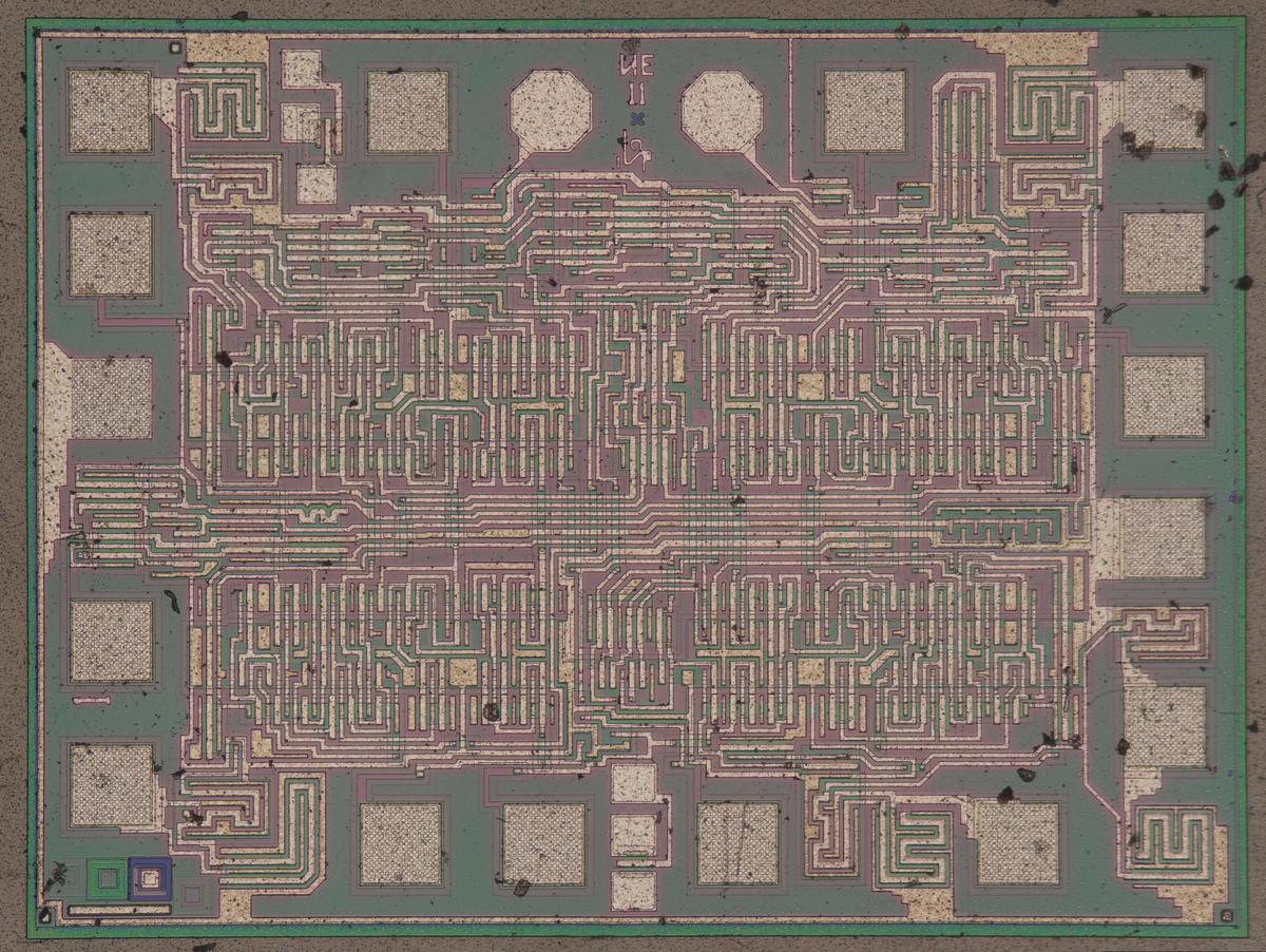
Die photo of the К561ИЕ11 chip on a wafer. Image courtesy of Martin Evtimov. Click this image (or any other) for a larger version.

Die photo of the К561ИЕ11 chip on a wafer. Image courtesy of Martin Evtimov. Click this image (or any other) for a larger version.

The photo above shows the tiny silicon die under a microscope. Regions of the silicon are doped with impurities to change the silicon's electrical properties. This doping also causes regions of the silicon to appear greenish or reddish, depending on how a region is doped. (These color changes will turn out to be useful for reverse engineering.) On top of the silicon, the whitish metal layer is visible, forming the chip's connections. This chip uses metal-gate transistors, an old technology, so the metal layer also forms the gates of the transistors. Around the outside of the chip, the 16 square bond pads connect the chip to the outside world. When installed in a package, the die has tiny bond wires between the pads and the lead frame, the metal structure that connects to the chip's pins.

According to the Russian datasheet,2 the chip has 319 "elements", presumably counting the semiconductor devices. The chip has a handful of diodes to protect the inputs, so the total transistor count is a bit over 300. This transistor count is nothing compared to a modern CMOS processor with tens of billions of transistors, of course, but most of the circuit principles are the same.

NMOS and PMOS transistors

CMOS is a low-power logic family now used in almost all processors.3 CMOS (complementary MOS) circuitry uses two types of transistors, NMOS and PMOS, working together. The diagram below shows how an NMOS transistor is constructed. The transistor can be considered a switch between the source and drain, controlled by the gate. The source and drain regions (red) consist of silicon doped with impurities to change its semiconductor properties, forming N+ silicon. The gate consists of an aluminum layer, separated from the silicon by a very thin insulating oxide layer.4 (These three layers—Metal, Oxide, Semiconductor—give the MOS transistor its name.) This oxide layer is an insulator, so there is essentially no current flow through the gate, one reason why CMOS is a low-power technology. However, the thin oxide layer is easily destroyed by static electricity, making MOS integrated circuits sensitive to electrostatic discharge.
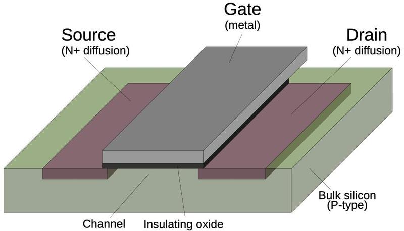
Structure of an NMOS transistor.

Structure of an NMOS transistor.

A PMOS transistor (below) has the opposite configuration from an NMOS transistor: the source and drain are doped to form P+ regions, while the underlying bulk silicon is N-type silicon. The doping process is interesting, but I'll leave the details to a footnote.5
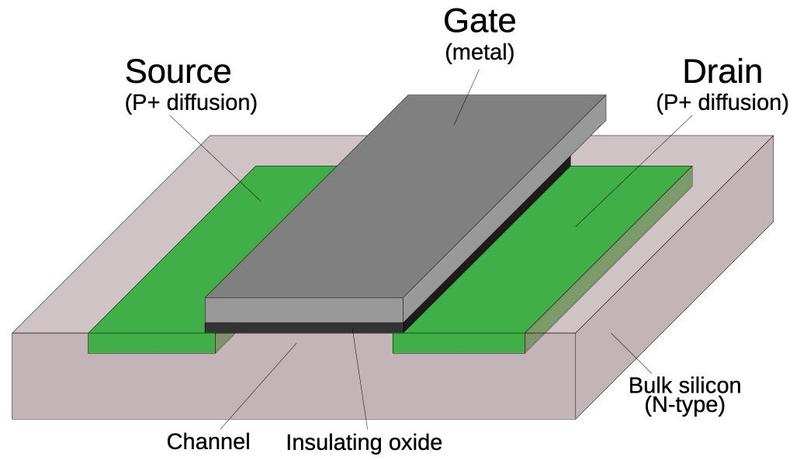
Structure of a PMOS transistor.

Structure of a PMOS transistor.

The NMOS and PMOS transistors are opposite in their construction and operation; this is the "Complementary" in CMOS. An NMOS transistor turns on when the gate is high, while a PMOS transistor turns on when the gate is low. An NMOS transistor is best at pulling its output low, while a PMOS transistor is best at pulling its output high. In a CMOS circuit, the transistors work as a team, pulling the output high or low as needed. The behavior of MOS transistors is complicated, so this description is simplified, just enough to understand digital circuits.

If you buy an MOS transistor from an electronics supplier, it comes as a package with three leads for the source, gate, and drain. The source and drain are connected differently inside the package and are not interchangeable in a circuit. In an integrated circuit, however, the transistor is symmetrical and the source and drain are the same. For that reason, I won't distinguish between the source and the drain in the following discussion. I will use the symmetrical symbols below for NMOS and PMOS transistors; the inversion bubble on the PMOS gate symbolizes that a low signal activates the PMOS transistor.
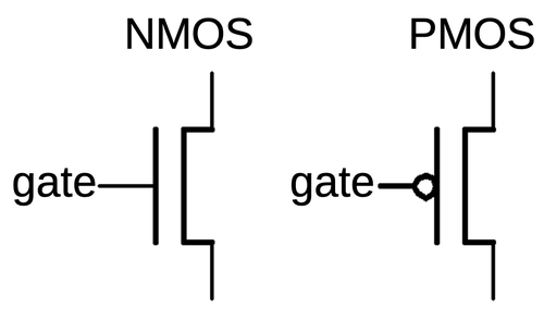
Symbols for NMOS and PMOS transistors.

Symbols for NMOS and PMOS transistors.

One complication is that NMOS transistors are built on P-type silicon, while PMOS transistors are built on N-type silicon. Since the silicon die itself is N silicon, the NMOS transistors need to be surrounded by a tub or well of P silicon.6 The cross-section diagram below shows how the NMOS transistor on the right is embedded in the well of P-type silicon. Constructing two transistor types with opposite behaviors makes manufacturing more complex, one reason why CMOS took years to catch on. CMOS was invented in 1963 at Fairchild Semiconductor, but RCA was the main proponent of CMOS, commercializing it in the late 1960s. Although RCA produced a CMOS microprocessor in 1974, mainstream microprocessors didn't switch to CMOS until the mid-1980s with chips such as the Motorola 68020 (1984) and the Intel 386 (1986).
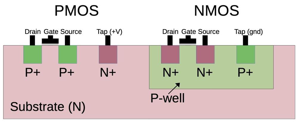
Cross-section of CMOS transistors.

Cross-section of CMOS transistors.

For proper operation, the silicon that surrounds transistors needs to be connected to the appropriate voltage through "tap" contacts.7 For PMOS transistors, the substrate is connected to power through the taps, while for NMOS transistors the well region is connected to ground through the taps. When reverse-engineering, the taps can provide important clues, indicating which regions are NMOS and which are PMOS. As will be seen below, these voltages are also important for understanding the circuitry of this chip.

The die photo below shows two transistors as they appear on the die. The appearance of transistors varies between different integrated circuits, so a first step of reverse engineering is determining how they look in a particular chip. In this IC, a transistor gate can be distinguished by a large rectangular region over the silicon. (In other metal-gate transistors, the gate often has a "bubble" appearance.) The interactions between the metal wiring and the silicon can be distinguished by subtle differences. For the most part, the metal wiring passes over the silicon, isolated by thick insulating oxide. A contact between metal and silicon is recognizable by a smaller oval region that is slightly darker; wires are connected to the transistor sources and drains below. MOS transistors often don't have discrete boundaries; as will be seen later, the source of one transistor can overlap with the drain of another.
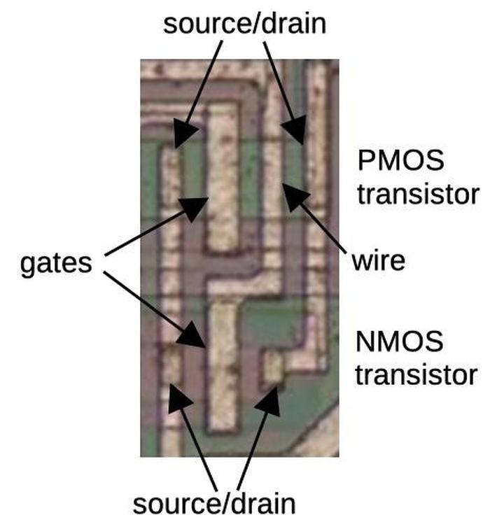
Two transistors on the die.

Two transistors on the die.

Distinguishing PMOS and NMOS transistors can be difficult. On this chip, P-type silicon appears greenish, and N-type silicon appears reddish. Thus, PMOS transistors appear as a green region surrounded by red, while NMOS is the opposite. Moreover, PMOS transistors are generally larger than NMOS transistors because they are weaker. Another way to distinguish them is by their connection in circuits. As will be seen below, PMOS transistors in logic gates are connected to power while NMOS transistors are connected to ground.

Metal-gate transistors are a very old technology, mostly replaced by silicon-gate transistors in the 1970s. Silicon-gate circuitry uses an additional layer of polysilicon wiring. Moreover, modern ICs usually have more than one layer of metal. The metal-gate IC in this post is easier to understand than a modern IC, since there are fewer layers to analyze. The CMOS principles are the same in modern ICs, but the layout will appear different.

Implementing an inverter in CMOS

The simplest CMOS gate is an inverter, shown below. Although basic, it illustrates most of the principles of CMOS circuitry. The inverter is constructed from a PMOS transistor on top to pull the output high and an NMOS transistor below to pull the output low. The input is connected to the gates of both transistors.
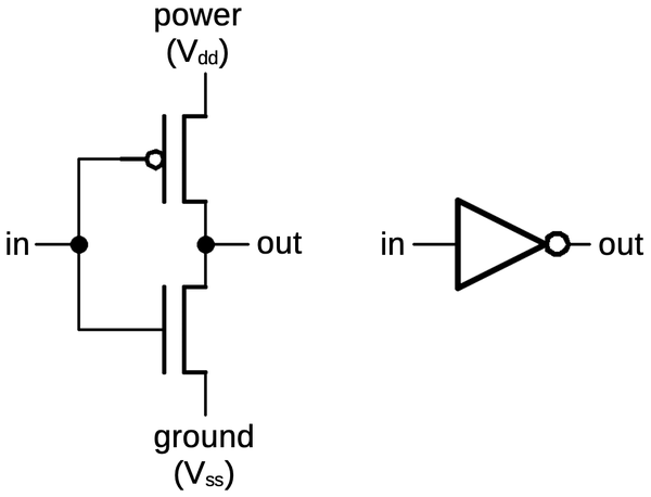
A CMOS inverter is constructed from a PMOS transistor (top) and an NMOS transistor (bottom).

A CMOS inverter is constructed from a PMOS transistor (top) and an NMOS transistor (bottom).

Recall that an NMOS transistor is turned on by a high signal on the gate, while a PMOS transistor is the opposite, turned on by a low signal. Thus, when the input is high, the NMOS transistor (bottom) turns on, pulling the output low. When the input is low, the PMOS transistor (top) turns on, pulling the output high. Notice how the transistors act in opposite (i.e. complementary) fashion.
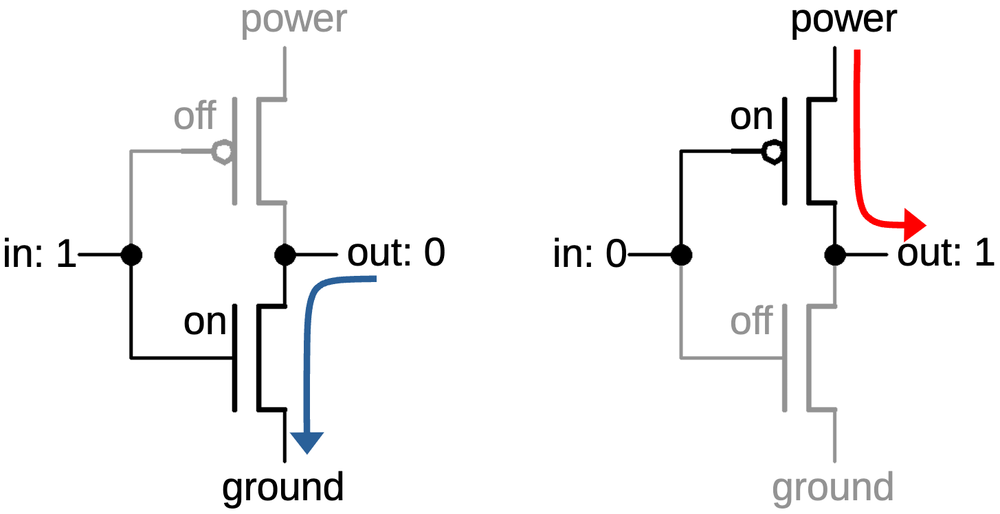
How the inverter functions.

How the inverter functions.

An inverter on the die is shown below. The PMOS and NMOS transistors are indicated by red boxes and the transistors are connected according to the schematics above. The input is connected to the gates of the two transistors, which can be distinguished as larger metal rectangles. On the right, two contacts connect the transistor drains to the output. The power and ground connections are a bit different from most chips since the metal lines appear to not go anywhere. The short metal line labeled "power" connects the PMOS transistor's source to the substrate, the reddish silicon that surrounds the transistor. As described earlier, the substrate is connected to the chip's power. Thus, the transistor receives its power through the substrate silicon. This approach isn't optimal, due to the relatively high resistance of silicon, but it simplifies the wiring. Similarly, the ground metal connects the NMOS transistor's source to the well that surrounds the transistor, P-type silicon that appears green. Since the well is grounded, the transistor has its ground connection.
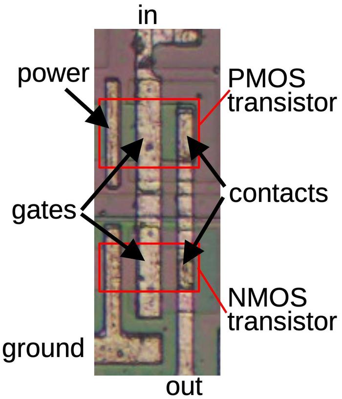
An inverter on the die.

An inverter on the die.

Some inverters look different from the layout above. Many of the chip's inverters are constructed as two inverters in parallel to provide twice the output current. This gives the inverter more "fan-out", the ability to drive the inputs of a larger number of gates.8 The diagram below shows a doubled inverter, which is essentially the previous inverter mirrored and copied, with two PMOS transistors at the top and two NMOS transistors at the bottom. Note that there is no explicit boundary between the paired transistors; their drains share the same silicon. Consequently, each output contact is shared between two transistors, rather than being duplicated.
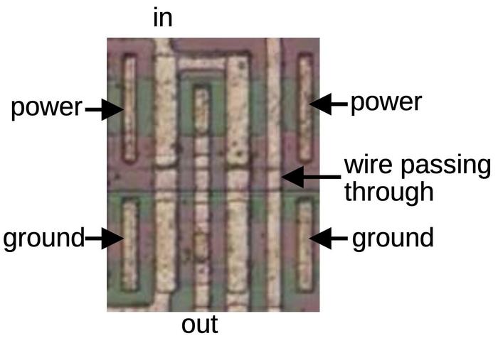
An inverter consisting of two inverters in parallel.

An inverter consisting of two inverters in parallel.

Another style of inverter drives the chip's output pins. The output pins require high current to drive external circuitry. The chip uses much larger transistors to provide this current. Nonetheless, the output driver uses the same inverter circuit described earlier, with a PMOS transistor to put the output high and an NMOS transistor to pull the output low. The photo below shows one of these output inverters on the die. To fit the larger transistors into the available space, the transistors have a serpentine layout, with the gate winding between the source and the drain. The inverter's output is connected to a bond pad. When the die is mounted in a package, tiny bond wires connect the pads to the external pins.
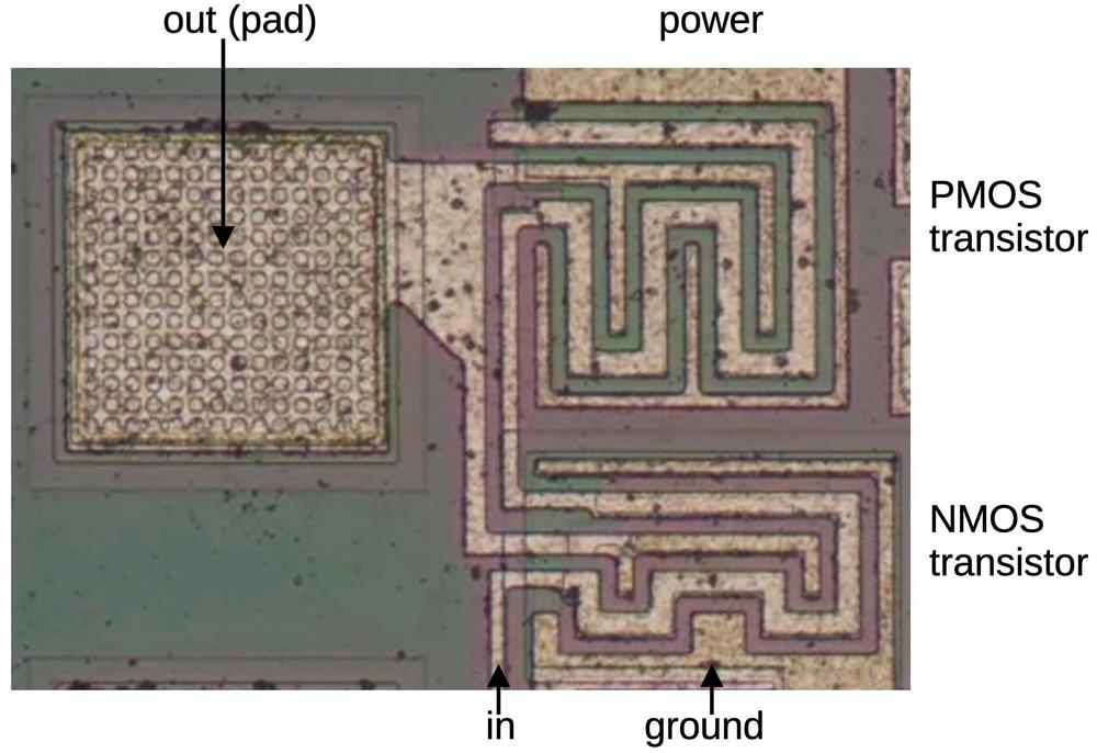
An output driver is an inverter, built with much larger transistors.

An output driver is an inverter, built with much larger transistors.

NOR and NAND gates

Other logic gates are constructed using the same concepts as the inverter, but with additional transistors. In a NOR gate, the PMOS transistors on top are in series, so the output will be pulled high if all inputs are 0. The NMOS transistors on the bottom are in parallel, so the output will be pulled low if any input is 1. Thus, the circuit implements the NOR function. Again, note the complementary action: the PMOS transistors pull the output high, while the NMOS transistors pull the output low. Moreover, the PMOS transistors are in series, while the NMOS transistors are in parallel. The circuit below is a 3-input NOR gate; different numbers of inputs are supported similarly. (With just one input, the circuit becomes an inverter, as you might expect.)
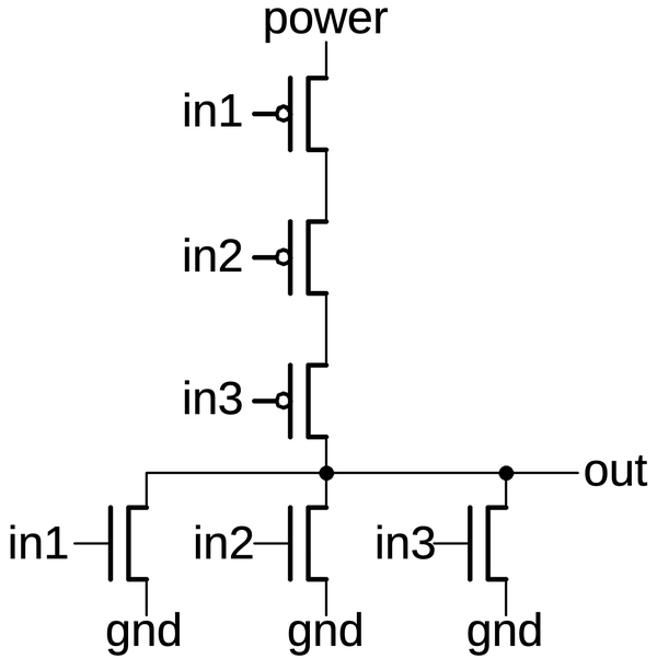
A 3-input NOR gate implemented in CMOS.

A 3-input NOR gate implemented in CMOS.

For any gate implementation, the input must be either pulled high by the PMOS side, or pulled low by the NMOS side. If both happen simultaneously for some input, power and ground would be shorted, possibly destroying the chip. If neither happens, the output would be floating, which is bad in a CMOS circuit.9 In the NOR gate above, you can see that for any input the output is always pulled either high or low as required. Reverse engineering tip: if the output is not always pulled high or low, you probably made a mistake in either the PMOS circuit or the NMOS circuit.10

The diagram below shows how a 3-input NOR gate appears on the die.11 The transistor gates are the thick vertical metal rectangles; PMOS transistors are on top and NMOS below. The three PMOS transistors are in series between power on the left and the output connection on the right. As with the inverter, the power and ground connections are wired to the bulk silicon, not to the chip's power and ground lines.
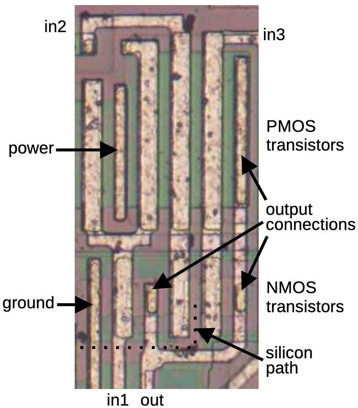
A 3-input NOR gate as it is implemented on the die. The "extra" PMOS transistor on the left is part of a different gate.

A 3-input NOR gate as it is implemented on the die. The "extra" PMOS transistor on the left is part of a different gate.

The layout of the NMOS transistors is more complicated because it is difficult to wire the transistors in parallel with just one layer of metal. The output wire connects between the first and second transistors as well as to the third transistor. An unusual feature is the connection of the second and third NMOS transistors to ground is done by a horizontal line of doped silicon (reddish "silicon path" indicated by the dotted line). This silicon extends from the ground metal to the region between the two transistors. Finally, note that the PMOS transistors are much larger than the NMOS transistors. This is both because PMOS transistors are inherently less efficient and because transistors in series need to be lower resistance to avoid degrading the output signal. Reverse-engineering tip: It's often easier to recognize the transistors in series and then use that information to determine which transistors must be in parallel.

A NAND gate is implemented by swapping the roles of the series and parallel transistors. That is, the PMOS transistors are in parallel, while the NMOS transistors are in series. For example, the schematic below shows a 4-input NAND gate. If all inputs are 1, the NMOS transistors will pull the output low. If any input is a 0, the corresponding PMOS transistor will pull the output high. Thus, the circuit implements the NAND function.
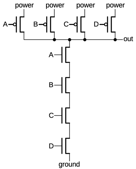
A 4-input NAND gate implemented in CMOS.

A 4-input NAND gate implemented in CMOS.

The diagram below shows a four-input NAND gate on the die. In the bottom half, four NMOS transistors are in series, while in the top half, four PMOS transistors are in parallel. (Note that the series and parallel transistors are switched compared to the NOR gate.) As in the NOR gate, the power and ground are provided by metal connections to the bulk silicon (two connections for the power). The parallel PMOS circuit uses a "silicon path" (green) to connect each transistor to the output without intersecting the metal. In the middle, this silicon has a vertical metal line on top; this reduces the resistance of the silicon path. The NMOS transistors are larger than the PMOS transistors in this case because the NMOS transistors are in series.
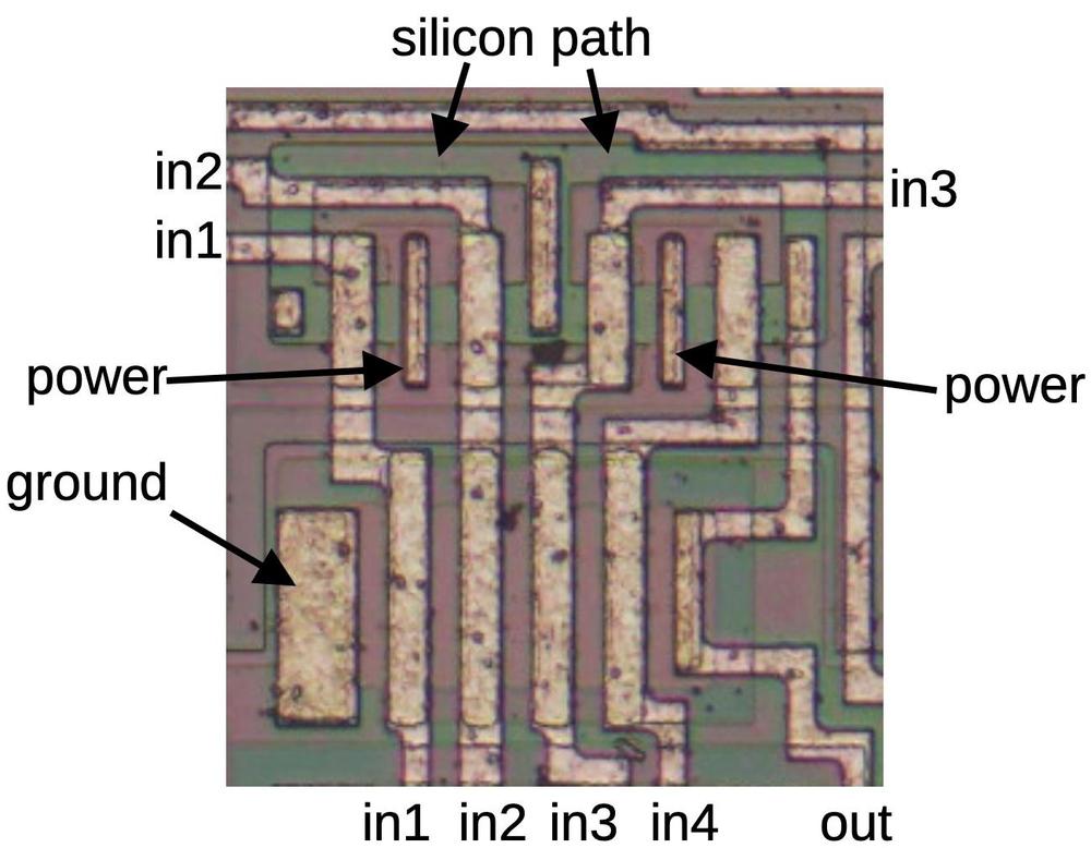
A four-input NAND gate as it appears on the die.

A four-input NAND gate as it appears on the die.

Complex gates

More complex gates such as AND-NOR (AND-OR-INVERT) can also be constructed in CMOS; these gates are commonly used because they are no harder to build than NAND or NOR gates. The schematic below shows an AND-NOR gate. To understand its construction, look at the paths to ground through the NMOS transistors. The first path is through A, B, and C. If these inputs are all high, the output is low, implementing the AND-INVERT side of the gate. The second path is through D, which will pull the output low by itself, implementing the OR-INVERT side of the gate. You can verify that the PMOS transistors pull the output high in the necessary circumstances. Observe that the D transistor is in series on the PMOS side and in parallel on the NMOS side, again showing the complementary nature of these circuits.
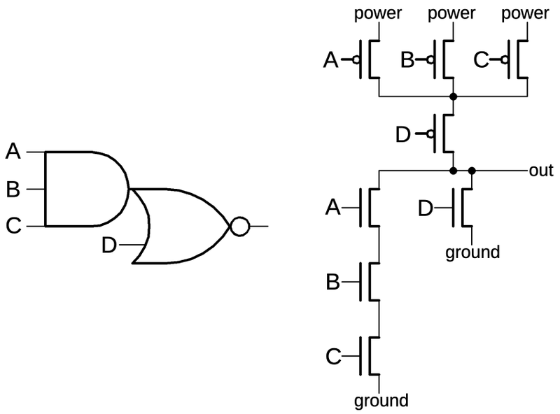
An AND-NOR gate.

An AND-NOR gate.

The diagram below shows this AND-NOR gate on the die, with the four inputs A, B, C, and D, corresponding to the schematic above. This gate has a few tricky layout features. The biggest surprise is that there is half of another gate (a 3-input NOR gate) in the middle of this gate. Presumably, the designers found this arrangement efficient since the other gate also uses inputs A, B, and C. The output of the other gate (D) is an input to the gate we're examining. Ignoring the other gate, the AND-NOR gate has the NMOS transistors in the first column, on top of a reddish band, and the PMOS transistors in the third column, on top of a greenish band. Hopefully you can recognize the transistor gates, the large rectangles connected to A, B, C, and D. Matching the schematic above, there are three NMOS transistors in series on the left, connected to A, B, and C, as well as the D transistor providing a second path between ground and the output. On the PMOS side, the A, B, and C transistors are in parallel, and then connected through the D transistor to the output. The green "silicon path" on the right provides the parallel connection from transistors A and B to transistors C and D. Most of this path is covered by two long metal regions, reducing the resistance. But in order to cross under wires B and C, the metal has a break where the green silicon provides the connection.
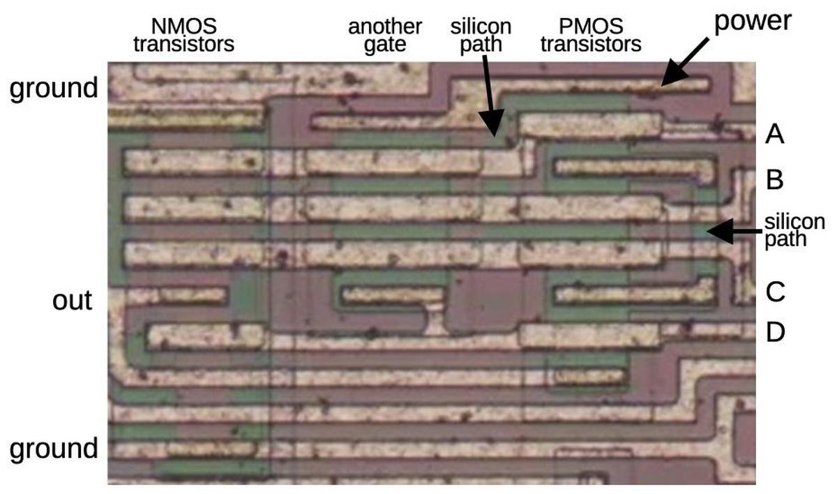
An AND-NOR gate on the die.

An AND-NOR gate on the die.

As with the other gates, the power is obtained by a connection to the bulk silicon, bridging the red and green regions. If you look closely, there is a green band ("silicon path") down from the power connection and joining the main green region between the B and C transistors, providing power to those transistors through the silicon. The NMOS transistors, on the other hand, have ground connections at the top and bottom. For this circuit, ground is supplied through solid metal wires at the top and the bottom, rather than a connection to the bulk silicon.

A few principles help when reverse-engineering logic gates. First, because of the complementary nature of CMOS, the output must either be pulled high by the PMOS transistors or pulled low by the NMOS transistors. Thus, one group or the other must be activated for each possible input. This implies that the same inputs must go to both the NMOS and PMOS transistors. Moreover, the structures of the NMOS and PMOS circuits are complementary: where the NMOS transistors are parallel, the PMOS transistors must be in series, and vice versa. In the case of the AND-NOR circuit above, these principles are helpful. For instance, you might not spot the "silicon paths", but since the PMOS half must be complementary to the NMOS half, you know that those connections must exist.

Even complex gates can be reverse-engineered by breaking the NMOS transistors into series and parallel groups, corresponding to AND and OR terms. Note that MOS transistors are inherently inverting, so a single gate will always end with inversion. Thus, you can build an AND-OR-AND-NOR gate for instance, but you can't build an AND gate as a single circuit.

Transmission gate

Another key circuit is the transmission gate. This acts as a switch, either passing a signal through or blocking it. The schematic below shows how a transmission gate is constructed from two transistors, an NMOS transistor and a PMOS transistor. If the enable line is high (i.e. low to the PMOS transistor) both transistors turn on, passing the input signal to the output. The NMOS transistor primarily passes a low signal, while the PMOS transistor passes a high signal, so they work together. If the enable line is low, both transistors turn off, blocking the input signal. The schematic symbol for a transmission gate is shown on the right. Note that the transmission gate is bidirectional; it doesn't have a specific input and output. Examining the surrounding circuitry usually reveals which side is the input and which side is the output.
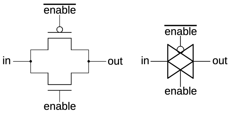
A transmission gate is constructed from two transistors. The transistors and their gates are indicated. The schematic symbol is on the right.

A transmission gate is constructed from two transistors. The transistors and their gates are indicated. The schematic symbol is on the right.

The photo below shows how a transmission gate appears on the die. It consists of a PMOS transistor at the top and an NMOS transistor at the bottom. Both the enable signal and the complemented enable signal are used, one for the NMOS transistor's gate and one for the PMOS transistor.
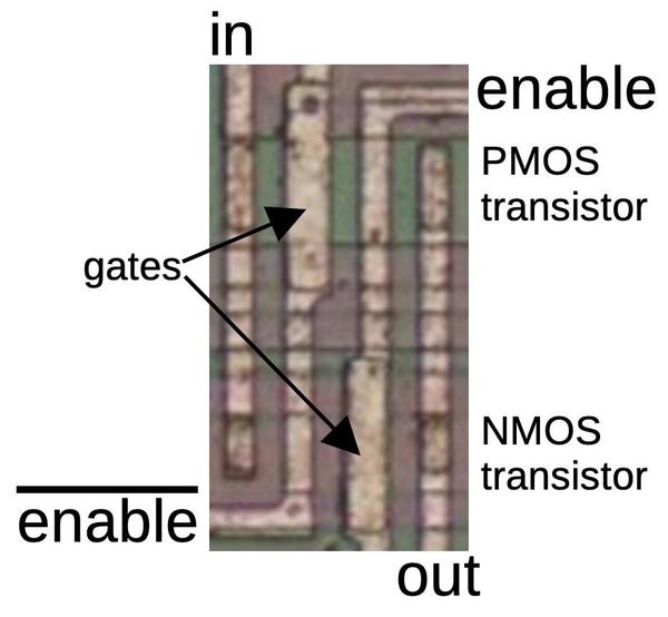
A transmission gate on the die, consisting of two transistors.

A transmission gate on the die, consisting of two transistors.

The inverter and transmission gate are both two-transistor circuits, but they can be easily distinguished for reverse engineering. One difference is that an inverter is connected to power and ground, while the transmission gate is unpowered. Moreover, the inverter has one input, while the transmission gate has three inputs (counting the control lines). In the inverter, both transistor gates have the same input, so one transistor turns on at a time. In the transmission gate, however, the gates have opposite inputs, so the transistors turn on or off together.

One useful circuit that can be built from transmission gates is the multiplexer, a circuit that selects one of two (or more) inputs. The multiplexer below selects either input inA or inB and connects it to the output, depending if the selection line selA is high or low respectively. The multiplexer can be built from two transmission gates as shown. Note that the select lines are flipped on the second transmission gate, so one transmission gate will be activated at a time. Multiplexers with more inputs can be built by using more transmission gates with additional select lines.
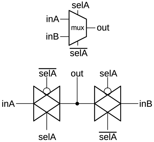
Schematic symbol for a multiplexer and its implementation with two transmission gates.

Schematic symbol for a multiplexer and its implementation with two transmission gates.

The die photo below shows a block of transmission gates consisting of six PMOS transistors and six NMOS transistors. The labels on the metal lines will make more sense as the reverse engineering progresses. Note that the metal layer provides much of the wiring for the circuit, but not all of it. Much of the wiring is implicit, in the sense that neighboring transistors are connected because the source of one transistor overlaps the drain of another.
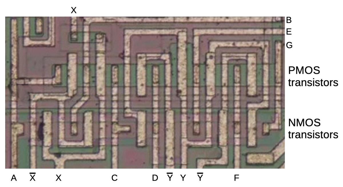
A block of transistors implementing multiple transmission gates.

A block of transistors implementing multiple transmission gates.

While this may look like an incomprehensible block of zig-zagging lines, tracing out the transistors will reveal the circuitry (below). The wiring in the schematic matches the physical layout on the die, so the schematic is a bit of a mess. With a single layer of metal for wiring, the layout becomes a bit convoluted to avoid crossing wires. (The only wire crossing in this image is in the upper left for wire X; the signal uses a short stretch of silicon to pass under the metal.)

Schematic of the previous block of transistors.

Schematic of the previous block of transistors.

Looking at the PMOS and NMOS transistors as pairs reveals that the circuit above is a chain of transmission gates (shown below). It's not immediately obvious which wires are inputs and which wires are outputs, but it's a good guess that pairs of transmission gates using the opposite control lines form a multiplexer. That is, inputs A and C are multiplexed to output B, inputs C and E are multiplexed to output D, and so forth. As will be seen, these transmission gates form multiplexers that are part of a flip-flop.

The transistors form six transmission gates.

The transistors form six transmission gates.

Latches and flip-flops

Flip-flops and latches are important circuits, able to hold one bit and controlled by a clock signal. Terminology is inconsistent, but I'll use flip-flop to refer to an edge-triggered device and latch to refer to a level-triggered device. That is, a flip-flop will grab its input at the moment the clock signal goes high (i.e. it uses the clock edge), store it, and provide it as the output, called Q for historical reasons. A latch, on the other hand, will take its input, store it, and output it as long as the clock is high (i.e. it uses the clock level). The latch is considered "transparent", since the input immediately appears on the output if the clock is high.

The distinction between latches and flip-flops may seem pedantic, but it is important. Flip-flops will predictably update once per clock cycle, while latches will keep updating as long as the clock is high. By connecting the output of a flip-flop through an inverter back to the input, you can create a toggle flip-flop, which will flip its state once per clock cycle, dividing the clock by two. (This example will be important shortly.) If you try the same thing with a transparent latch, it will oscillate: as soon as the output flips, it will feed back to the latch input and flip again.

The schematic below shows how a latch can be implemented with transmission gates. When the clock is high, the first transmission gate passes the input through to the inverters and the output. When the clock is low, the second transmission gate creates a feedback loop for the inverters, so they hold their value, providing the latch action. Below, the same circuit is drawn with a multiplexer, which may be easier to understand: either the input or the feedback is selected for the inverters.
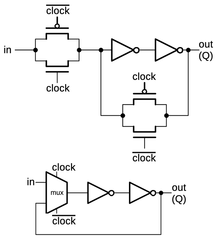
A latch implemented from transmission gates. Below, the same circuit is shown with a multiplexer.

A latch implemented from transmission gates. Below, the same circuit is shown with a multiplexer.

An edge-triggered flip-flop can be created by combining two latches in a primary/secondary arrangement. When the clock is low, the input will pass into the primary latch. When the clock switches high, two things happen. The primary latch will hold the current value of the input. Meanwhile, the secondary latch will start passing its input (the value from the primary latch) to its output, and thus the flip-flop output. The effect is that the flip-flop's output will be the value at the moment the clock goes high, and the flip-flop is insensitive to changes at other times. (The primary latch's value can keep changing while the clock is low, but this doesn't affect the flip-flop's output.)

Two latches, combined to form a flip-flop.

Two latches, combined to form a flip-flop.

The flip-flops in the counter chip are based on the above design, but they have two additional features. First, the flip-flop can be loaded with a value under the control of a Preset Enable (PE) signal. Second, the flip-flop can either hold its current value or toggle its value, under the control of a Toggle (T) signal. Implementing these features requires two more multiplexers in the primary latch as shown below. The first multiplexer selects either the inverted output or uninverted output to be fed back into the flip flop, providing the selectable toggle action. The second multiplexer is the latch's standard clocked multiplexer. The third multiplexer allows a "preset" value to be loaded directly into the flip-flop, bypassing the clock. (The preset value is inverted, since there are three inverters between the preset and the output.) The secondary latch is the same as before, except it provides the inverted and non-inverted outputs as feedback, allowing the flip-flop to either hold or toggle its value. This circuit illustrates how more complex flip-flops can be created from the building blocks that we've seen.

Schematic of the toggle flip-flop.

Schematic of the toggle flip-flop.

The gray letters in the schematic above match the earlier multiplexer diagram, showing how the three multiplexers were implemented on the die. The other multiplexer and the inverters are implemented in another block of circuitry. I won't explain that circuitry in detail since it doesn't illustrate any new principles.

Routing in silicon: cross-unders

With just one metal layer for wiring, routing of signals on the chip is difficult and requires careful planning. Even so, there are some cases where one signal must cross another. This is accomplished by using silicon for a "cross-under", allowing a signal to pass underneath metal wiring. These cross-unders are avoided unless necessary because silicon has much higher resistance than metal. Moreover, the cross-under requires additional space on the die.
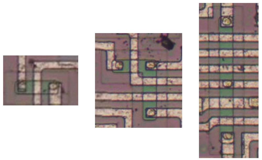
Three cross-unders on the die.

Three cross-unders on the die.

The images above show three cross-unders. In each one, signals are primarily routed in the metal layer, but a signal passes under the metal using a doped silicon region (which appears green). The first cross-under simply lets one signal cross under the second. The second image shows a signal branching as well as crossing under two signals. The third image shows a cross-under distributing a horizontal signal to the upper and lower halves of the chip, while crossing under multiple horizontal signals. Note the small oval contact between the green silicon region and the horizontal metal line, connecting them. It is easy to miss the small contact and think that the vertical signal is simply crossing under the horizontal signal, rather than branching.

About the chip

The focus of this article is the CMOS reverse engineering process rather than this specific chip, but I'll give a bit of information about the chip. The die has the Cyrillic characters ИЕ11 at the top indicating that the chip is a К561ИЕ11 or К564ИЕ11.12 The Soviet Union came up with a standardized numbering system for integrated circuits in 1968. This system is much more helpful than the American system of semi-random part numbers. In this part number, the 5 indicates a monolithic integrated circuit, while 61 or 64 is the series, specifically commercial-grade or military-grade clones of 4000 series CMOS logic. The character И indicates a digital circuit, while ИЕ is a counter. Thus, the part number systematically indicates that the integrated circuit is a CMOS counter.

The 561ИЕ11 turns out to be a copy of the Motorola MC14516 binary up/down counter.13 Conveniently, the Motorola datasheet provides a schematic (below). I won't explain the schematic in detail, but a quick overview may be helpful. The chip is a four-bit counter that can count up or down, and the heart of the chip is the four toggle flip-flops (red). To count up, a flip-flop is toggled if there is a carry from the lower bits, while counting down toggles a flip-flop if there is a borrow from the lower bits. (Much like base-10 long addition or subtraction.) The AND/NOR gates at the bottom (blue) look complex, but they are just generating the toggle signal T: toggle if the lower bits are all-1's and you're counting up, or if the lower bits are all-0's and you're counting down. The flip-flops can also be loaded in parallel from the P inputs. Additional logic allows the chips to be cascaded to form arbitrarily large counters; the carry-out pin of one chip is connected to the carry-in of the next.
Logic diagram of the MC14516 up/down counter chip, from the datasheet.

Logic diagram of the MC14516 up/down counter chip, from the datasheet.

I've labeled the die photo below with the pin functions and the functional blocks. Each quadrant of the chip handles one bit of the counter in a roughly symmetrical way. This quadrant layout accounts for the pin arrangement which otherwise appears semi-random with bits 3 and 0 on one side and bits 2 and 1 on the other, with inputs and output pins jumbled together. The toggle and carry logic is squeezed into the top and middle of the chip. You may recognize the large inverters next to each output pin. When reverse-engineering, look for large transistors next to pads to determine which pins are outputs.
The die with pins and functional blocks labeled.

The die with pins and functional blocks labeled.

Conclusions

This article has discussed the basic circuits that can be found in a CMOS chip. Although the counter chip is old and simple, later chips use the same principles. An important change in later chips is the introduction of silicon-gate transistors, which use polysilicon for the transistor gates and for an additional wiring layer. The circuits are the same, but you need to be able to recognize the polysilicon layer. Many chips have more than one metal layer, which makes it very hard to figure out the wiring connections. Finally, when the feature size approaches the wavelength of light, optical microscopes break down. Thus, these reverse-engineering techniques are only practical up to a point. Nonetheless, many interesting CMOS chips can be studied and reverse-engineered.

For more, follow me on Twitter @kenshirriff or RSS for updates. I'm also on Mastodon as @kenshirriff@oldbytes.space. Thanks to Martin Evtimov for providing the die photos.

Notes and references

  1. I'm not sure of the date and manufacturing location of the chip. I think the design is old, from the Soviet Union. (Motorola introduced the MC14516 around 1972 but I don't know when it was copied.) The wafer is said to be scrap from a Ukrainian manufacturer so it may have been manufactured more recently. The die has a symbol that might be a manufacturing logo, but nobody on Twitter could identify it.
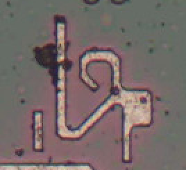
    A symbol that appears on the die.

    A symbol that appears on the die.


  2. For more about this chip, the Russian databook can be downloaded here; see Volume 5 page 501. 

  3. Early CMOS microprocessors include the 8-bit RCA 1802 COSMAC (1974) and the 12-bit Intersil 6100 (1974). The 1802 is said to be the first CMOS microprocessor. Mainstream microprocessors didn't switch to CMOS until the mid-1980s. 

  4. The chip in this article has metal-gate transistors, with aluminum forming the transistor gate. These transistors were not as advanced as the silicon-gate transistors that were developed in the late 1960s. Silicon gate technology was much better in several ways. First, silicon-gate transistors were smaller, faster, more reliable, and used lower voltages. Second, silicon-gate chips have a layer of polysilicon wiring in addition to the metal wiring; this made chip layouts about twice as dense. 

  5. To produce N-type silicon, the silicon is doped with small amounts of an element such as phosphorus or arsenic. In the periodic table, these elements are one column to the right of silicon so they have one "extra" electron. The free electrons move through the silicon, carrying charge. Because electrons are negative, this type of silicon is called N-type. Conversely, to produce P-type silicon, the silicon is doped with small quantities of an element such as boron. Since boron is one column to the left of silicon in the periodic table, it has one fewer free electrons. A strange thing about semiconductor physics is that the missing electrons (called holes) can move around the silicon much like electrons, but carrying positive charge. Since the charge carriers are positive, this type of silicon is called P-type. For various reasons, electrons carry charge better than holes, so NMOS transistors work better than PMOS transistors. As a result, PMOS transistors need to be about twice the size of comparable NMOS transistors. This quirk is useful for reverse engineering, since it can help distinguish NMOS and PMOS transistors.

    The amount of doping required can be absurdly small, 20 atoms of boron for every billion atoms of silicon in some cases. A typical doping level for N-type silicon is 1015 atoms of phosphorus or arsenic per cubic centimeter, which sounds like a lot until you realize that pure silicon consists of 5×10²² atoms per cubic centimeter. A heavily doped P+ region might have 1020 dopant atoms per cubic centimeter, one atom of boron per 500 atoms of silicon. (Doping levels are described here.) 

  6. This chip is built on a substrate of N-type silicon, with wells of P-type silicon for the NMOS transistors. Chips can be built the other way around, starting with P-type silicon and putting wells of N-type silicon for the PMOS transistors. Another approach is the "twin-well" CMOS process, constructing wells for both NMOS and PMOS transistors. 

  7. The bulk silicon voltage makes the boundary between a transistor and the bulk silicon act as a reverse-biased diode, so current can't flow across the boundary. Specifically, for a PMOS transistor, the N-silicon substrate is connected to the positive supply. For an NMOS transistor, the P-silicon well is connected to ground. A P-N junction acts as a diode, with current flowing from P to N. But the substrate voltages put P at ground and N at +5, blocking any current flow. The result is that the bulk silicon can be considered an insulator, with current restricted to the N+ and P+ doped regions. If this back bias gets reversed, for example, due to power supply fluctuations, current can flow through the substrate. This can result in "latch-up", a situation where the N and P regions act as parasitic NPN and PNP transistors that latch into the "on" state. This shorts power and ground and can destroy the chip. The point is that the substrate voltages are very important for proper operation of the chip. 

  8. Many inverters in this chip duplicate the transistors to increase the current output. The same effect could be achieved with single transistors with twice the gate width. (That is, twice the height in the diagrams.) Because these transistors are arranged in uniform rows, doubling the transistor height would mess up the layout, so using more transistors instead of changing the size makes sense. 

  9. Some chips use dynamic logic, in which case it is okay to leave the gate floating, neither pulled high nor low. Since the gate resistance is extremely high, the capacitance of a gate will hold its value (0 or 1) for a short time. After a few milliseconds, the charge will leak away, so dynamic logic must constantly refresh its signals before they decay.

    In general, the reason you don't want an intermediate voltage as the input to a CMOS circuit is that the voltage might end up turning the PMOS transistor partially on while also turning the NMOS transistor partially on. The result is high current flow from power to ground through the transistors. 

  10. One of the complicated logic gates on the die didn't match the implementation I expected. In particular, for some inputs, the output is neither pulled high nor low. Tracing the source of these inputs reveals what is going on: the gate takes both a signal and its complement as inputs. Thus, some of the "theoretical" inputs are not possible; these can't be both high or both low. The logic gate is optimized to ignore these cases, making the implementation simpler. 

  11. This schematic explains the physical layout of the 3-input NOR gate on the die, in case the wiring isn't clear. Note that the PMOS transistors are wired in series and the NMOS transistors are in parallel, even though both types are physically arranged in rows.
    The 3-input NOR gate on the die. This schematic matches the physical layout.

    The 3-input NOR gate on the die. This schematic matches the physical layout.


  12. The commercial-grade chips and military-grade chips presumably use the same die, but are distinguished by the level of testing. So we can't categorize the die as 561-series or 564-series. 

  13. Motorola introduced the MC14500 series in 1971 to fill holes in the CD4000 series. For more about this series, see A Strong Commitment to Complementary MOS

Interesting double-poly latches inside AMD's vintage LANCE Ethernet chip

I've studied a lot of chips from the 1970s and 1980s, so I usually know what to expect. But an Ethernet chip from 1982 had something new: a strange layer of yellow wiring on the die. After some study, I learned that the yellow wiring is a second layer of resistive polysilicon, used in the chip's static storage cells and latches.

A closeup of the die of the LANCE chip. The metal has been removed to show the layers underneath.

A closeup of the die of the LANCE chip. The metal has been removed to show the layers underneath.

The die photo above shows a closeup of a latch circuit, with the diagonal yellow stripe in the middle. For this photo, I removed the chip's metal layer so you can see the underlying circuitry. The bottom layer, silicon, appears gray-purple under the microscope, with the active silicon regions slightly darker and bordered in black. On top of the silicon, the pink regions are polysilicon, a special type of silicon. Polysilicon has a critical role in the chip: when it crosses active silicon, polysilicon forms the gate of a transistor. The circles are contacts between the metal layer and the underlying silicon or polysilicon. So far, the components of the chip match most NMOS chips of that time. But what about the bright yellow line crossing the circuit diagonally? That was new to me. This second layer of polysilicon provides resistance. It crosses over the other layers, connected to the silicon at the ends with a complex ring structure.

Why would you want high-resistance wiring in your digital chip? To understand this, let's first look at how a bit can be stored. An efficient way to store a bit is to connect two inverters in a loop, as shown below. Each inverter sends the opposite value to the other inverter, so the circuit will be stable in two states, holding one bit: a 1 or a 0.

Two cross-coupled inverters can store either a 0 or a 1 bit.

Two cross-coupled inverters can store either a 0 or a 1 bit.

But how do you store a new value into the inverter loop? There are a few techniques. One is to use pass transistors to break the loop, allowing a new value to be stored. In the schematic below, if the hold signal is activated, the transistor turns on, completing the loop. But if hold is dropped and load is activated, a new value can be loaded from the input into the inverter loop.

A latch, controlled by pass transistors.

A latch, controlled by pass transistors.

An alternative is to use a weak inverter that produces a low-current output. In this case, the input signal can simply overpower the value produced by the inverter, forcing the loop into a new state. The advantage of this circuit is that it eliminates the "hold" transistor. However, a weak inverter turns out to be larger than a regular inverter, negating much of the space saving.1 (The Intel 386 processor uses this type of latch.)

A latch using a weak inverter.

A latch using a weak inverter.

A third alternative, used in the Ethernet chip, is to use a resistor for the feedback, limiting the current.2 As in the previous circuit, the input can overpower the low feedback current. However, this circuit is more compact since it doesn't require a larger inverter. The resistor doesn't require additional space since it can overlap the rest of the circuitry, as shown in the photo at the top of the article. The disadvantage is that manufacturing the die requires additional processing steps to create the resistive polysilicon layer.

A latch using a resistor for feedback.

A latch using a resistor for feedback.

In the Ethernet chip, this type of latch is used in many circuits. For example, shift registers are built by connecting latches in sequence, controlled by the clock signals. Latches are also used to create binary counters, with the latch value toggled when the lower bits produce a carry.

The SRAM cell

It would be overkill to create a separate polysilicon layer just for a few latches. It turns out that the chip was constructed with AMD's "64K dynamic RAM process". Dynamic RAM uses tiny capacitors to store data. In the late 1970s, dynamic RAM chips started using a "double-poly" process with one layer of polysilicon to form the capacitors and a second layer of polysilicon for transistor gates and wiring (details).

The double-poly process was also useful for shrinking the size of static RAM.3 The Ethernet chip contains several blocks of storage buffers for various purposes. These blocks are implemented as static RAM, including a 22×16 block, a 48×9 block, and a 16×7 block. The photo below shows a closeup of some storage cells, showing how they are arranged in a regular grid. The yellow lines of resistive polysilicon are visible in each cell.

A block of 28 storage cells in the chip. Some of the second polysilicon layer is damaged.

A block of 28 storage cells in the chip. Some of the second polysilicon layer is damaged.

A static RAM storage cell is roughly similar to the latch cell, with two inverters in a loop to store each bit. However, the storage is arranged in a grid: each row corresponds to a particular word, and each column corresponds to the bits in a word. To select a word, a word select line is activated, turning on the pass transistors in that row. Reading and writing the cell is done through a pair of bitlines; each bit has a bitline and a complemented bitline. To read a word, the bits in the word are accessed through the bitlines. To write a word, the new value and its complement are applied to the bitlines, forcing the inverters into the desired state. (The bitlines must be driven with a high-current signal that can overcome the signal from the inverters.)

Schematic of one storage cell.

Schematic of one storage cell.

The diagram below shows the physical layout of one memory cell, consisting of two resistors and four transistors. The black lines indicate the vertical metal wiring that was removed. The schematic on the right corresponds to the physical arrangement of the circuit. Each inverter is constructed from a transistor and a pull-up resistor, and the inverters are connected into a loop. (The role of these resistors is completely different from the feedback resistors in the latch.) The two transistors at the bottom are the pass transistors that provide access to the cell for reads or writes.

One memory cell static memory cell as it appears on the die, along with its schematic.

One memory cell static memory cell as it appears on the die, along with its schematic.

The layout of this storage cell is highly optimized to minimize its area. Note that the yellow resistors take almost no additional area, as they overlap other parts of the cell. If constructed without resistors, each inverter would require an additional transistor, making the cell larger.

To summarize, although the double-poly process was introduced for DRAM capacitors, it can also be used for SRAM cell pull-up resistors. Reducing the size of the SRAM cells was probably the motivation to use this process for the Ethernet chip, with the latch feedback resistors a secondary benefit.

The Am7990 LANCE Ethernet chip

I'll wrap up with some background on the AMD Ethernet chip. Ethernet was invented in 1973 at Xerox PARC and became a standard in 1980. Ethernet was originally implemented with a board full of chips, mostly TTL. By the early 1980s, companies such as Intel, Seeq, and AMD introduced chips to put most of the circuitry onto VLSI chips. These chips reduced the complexity of Ethernet interface hardware, causing the price to drop from $2000 to $1000.

The chip that I'm examining is AMD's Am7990 LANCE (Local Area Network Controller for Ethernet). This chip implemented much of the functionality for Ethernet and "Cheapernet" (now known as 10BASE2 Ethernet). The chip handles serial/parallel conversion, computing the 32-bit CRC checksum, handling collisions and backoff, and recognizing desired addresses. The chip also provides DMA access for interfacing with a microcomputer.

The chip doesn't handle everything, though. It was designed to work with an Am7992 Serial Interface Adapter chip that encodes and decodes the bitstream using Manchester encoding. The third chip was the Am7996 transceiver that handled the low-level signaling and interfacing with the coaxial network cable, as well as detecting collisions if two nodes transmitted at the same time.

The LANCE chip is fairly complicated. The die photo below shows the main functional blocks of the chip. The chip is controlled by the large block of microcode ROM in the lower right. The large dark rectangles are storage, implemented with the static RAM cells described above. The chip has 48 pins, connected by tiny bond wires to the square pads around the edges of the die.

Main functional blocks of the LANCE chip.

Main functional blocks of the LANCE chip.

Thanks to Robert Garner for providing the AMD LANCE chip and information, thanks to a bunch of people on Twitter for discussion, and thanks to Bob Patel for providing the functional block labeling and other information. For more, follow me on Twitter @kenshirriff or RSS for updates. I'm also on Mastodon occasionally as @kenshirriff@oldbytes.space.

Notes and references

  1. It may seem contradictory for a weak inverter to be larger than a regular inverter, since you'd expect that the bigger the transistor, the stronger the signal. It turns out, however, that creating a weak signal requires a larger transistor, due to how MOS transistors are constructed. The current from a transistor is proportional to the gate's width divided by the length. Thus, to create a more powerful transistor, you increase the width. But to create a weak transistor, you can't decrease the width because the minimum width is limited by the manufacturing process. Thus, you need to increase the gate's length. The result is that both stronger and weaker transistors are larger than "normal" transistors. 

  2. You might worry that the feedback resistor will wastefully dissipate power. However, the feedback current is essentially zero because NMOS transistor gates are essentially insulators. Thus, the resistor only needs to pass enough current to charge or discharge the gate. 

  3. An AMD patent describes the double-poly process as well as the static RAM cell; I'm not sure this is the process used in the Ethernet chip, but I expect the process is similar. The diagram below shows the RAM cell with its two resistors. The patent describes how the resistors and second layer of wiring are formed by a silicide/polysilicon ("inverted polycide") sandwich. (The silicide is a low-resistance compound of tantalum and silicon or molybdenum and silicon.) Specifically, the second layer consists of a buffer layer of polysilicon, a thicker silicide layer, and another layer of polysilicon forming the low-resistance "sandwich". Where resistance is desired, the bottom two layers of "sandwich" are removed during fabrication to leave just a layer of polysilicon. This polysilicon is then doped through implantation to give it the desired resistance.

    The static RAM cell from patent 4569122, "Method of forming a low resistance quasi-buried contact".

    The static RAM cell from patent 4569122, "Method of forming a low resistance quasi-buried contact".

    The patent also describes using the second layer of polysilicon to provide a connection between silicon and the main polysilicon layer. Chips normally use a "buried contact" to connect silicon and polysilicon, but the patent describes how putting the second layer of polysilicon on top reduces the alignment requirements for a low-resistance contact. I think this explains the yellow ring of polysilicon around all the silicon/polysilicon contacts in the chip. (These rings are visible in the die photo at the top of the article.) Patent 4581815 refines this process further.


Two interesting XOR circuits inside the Intel 386 processor

Intel's 386 processor (1985) was an important advance in the x86 architecture, not only moving to a 32-bit processor but also switching to a CMOS implementation. I've been reverse-engineering parts of the 386 chip and came across two interesting and completely different circuits that the 386 uses to implement an XOR gate: one uses standard-cell logic while the other uses pass-transistor logic. In this article, I take a look at those circuits.

The die of the 386. Click this image (or any other) for a larger version.

The die of the 386. Click this image (or any other) for a larger version.

The die photo above shows the two metal layers of the 386 die. The polysilicon and silicon layers underneath are mostly hidden by the metal. The black dots around the edges are the bond wires connecting the die to the external pins. The 386 is a complicated chip with 285,000 transistor sites. I've labeled the main functional blocks. The datapath in the lower left does the actual computations, controlled by the microcode ROM in the lower right.

Despite the complexity of the 386, if you zoom in enough, you can see individual XOR gates. The red rectangle at the top (below) is a shift register for the chip's self-test. Zooming in again shows the silicon for an XOR gate implemented with pass transistors. The purple outlines reveal active silicon regions, while the stripes are transistor gates. The yellow rectangle zooms in on part of the standard-cell logic that controls the prefetch queue. The closeup shows the silicon for an XOR gate implemented with two logic gates. Counting the stripes shows that the first XOR gate is implemented with 8 transistors while the second uses 10 transistors. I'll explain below how these transistors are connected to form the XOR gates.

The die of the 386, zooming in on two XOR gates.

The die of the 386, zooming in on two XOR gates.

A brief introduction to CMOS

CMOS circuits are used in almost all modern processors. These circuits are built from two types of transistors: NMOS and PMOS. These transistors can be viewed as switches between the source and drain controlled by the gate. A high voltage on the gate of an NMOS transistor turns the transistor on, while a low voltage on the gate of a PMOS transistor turns the transistor on. An NMOS transistor is good at pulling the output low, while a PMOS transistor is good at pulling the output high. Thus, NMOS and PMOS transistors are opposites in many ways; they are complementary, which is the "C" in CMOS.

Structure of a MOS transistor. Although the transistor's name represents the Metal-Oxide-Semiconductor layers, modern MOS transistors typically use polysilicon instead of metal for the gate.

Structure of a MOS transistor. Although the transistor's name represents the Metal-Oxide-Semiconductor layers, modern MOS transistors typically use polysilicon instead of metal for the gate.

In a CMOS circuit, the NMOS and PMOS transistors work together, with the NMOS transistors pulling the output low as needed while the PMOS transistors pull the output high. By arranging the transistors in different ways, different logic gates can be created. The diagram below shows a NAND gate constructed from two PMOS transistors (top) and two NMOS transistors (bottom). If both inputs are high, the NMOS transistors turn on and pull the output low. But if either input is low, a PMOS transistor will pull the output high. Thus, the circuit below implements a NAND gate.

A NAND gate implemented in CMOS.

A NAND gate implemented in CMOS.

Notice that NMOS and PMOS transistors have an inherent inversion: a high input produces a low (for NMOS) or a low input produces a high (for PMOS). Thus, it is straightforward to produce logic circuits such as an inverter, NAND gate, NOR gate, or an AND-OR-INVERT gate. However, producing an XOR (exclusive-or) gate doesn't work with this approach: an XOR gate produces a 1 if either input is high, but not both.1 The XNOR (exclusive-NOR) gate, the complement of XOR, also has this problem. As a result, chips often have creative implementations of XOR gates.

The standard-cell two-gate XOR circuit

Parts of the 386 were implemented with standard-cell logic. The idea of standard-cell logic is to build circuitry out of standardized building blocks that can be wired by a computer program. In earlier processors such as the 8086, each transistor was carefully positioned by hand to create a chip layout that was as dense as possible. This was a tedious, error-prone process since the transistors were fit together like puzzle pieces. Standard-cell logic is more like building with LEGO. Each gate is implemented as a standardized block and the blocks are arranged in rows, as shown below. The space between the rows holds the wiring that connects the blocks.

Some rows of standard-cell logic in the 386 processor. This is part of the segment descriptor control circuitry.

Some rows of standard-cell logic in the 386 processor. This is part of the segment descriptor control circuitry.

The advantage of standard-cell logic is that it is much faster to create a design since the process can be automated. The engineer described the circuit in terms of the logic gates and their connections. A computer algorithm placed the blocks so related blocks are near each other. An algorithm then routed the circuit, creating the wiring between the blocks. These "place and route" algorithms are challenging since it is an extremely difficult optimization problem, determining the best locations for the blocks and how to pack the wiring as densely as possible. At the time, the algorithm took a day on a powerful IBM mainframe to compute the layout. Nonetheless, the automated process was much faster than manual layout, cutting weeks off the development time for the 386. The downside is that the automated layout is less dense than manually optimized layout, with a lot more wasted space. (As you can see in the photo above, the density is low in the wiring channels.) For this reason, the 386 used manual layout for circuits where a dense layout was important, such as the datapath.

In the 386, the standard-cell XOR gate is built by combining a NOR gate with an AND-NOR gate as shown below.2 (Although AND-NOR looks complicated, it is implemented as a single gate in CMOS.) You can verify that if both inputs are 0, the NOR gate forces the output low, while if both inputs are 1, the AND gate forces the output low, providing the XOR functionality.

Schematic of an XOR circuit.

Schematic of an XOR circuit.

The photo below shows the layout of this XOR gate as a standard cell. I have removed the metal and polysilicon layers to show the underlying silicon. The outlined regions are the active silicon, with PMOS above and NMOS below. The stripes are the transistor gates, normally covered by polysilicon wires. Notice that neighboring transistors are connected by shared silicon; there is no demarcation between the source of one transistor and the drain of the next.

The silicon implementing the XOR standard cell. This image is rotated 180° from the layout on the die to put PMOS at the top.

The silicon implementing the XOR standard cell. This image is rotated 180° from the layout on the die to put PMOS at the top.

The schematic below corresponds to the silicon above. Transistors a, b, c, and d implement the first NOR gate. Transistors g, h, i, and j implement the AND part of the AND-NOR gate. Transistors e and f implement the NOR input of the AND-NOR gate, fed from the first NOR gate. The standard cell library is designed so all the cells are the same height with a power rail at the top and a ground rail at the bottom. This allows the cells to "snap together" in rows. The wiring inside the cell is implemented in polysilicon and the lower metal layer (M1), while the wiring between cells uses the upper metal layer (M2) for vertical connections and lower metal (M1) for horizontal connections. This strategy allows vertical wires to pass over the cells without interfering with the cell's wiring.

Transistor layout in the XOR standard cell.

Transistor layout in the XOR standard cell.

One important factor in a chip such as the 386 is optimizing the sizes of transistors. If a transistor is too small, it will take too much time to switch its output line, reducing performance. But if a transistor is too large, it will waste power as well as slowing down the circuit that is driving it. Thus, the standard-cell library for the 386 includes several XOR gates of various sizes. The diagram below shows a considerably larger XOR standard cell. The cell is the same height as the previous XOR (as required by the standard cell layout), but it is much wider and the transistors inside the cell are taller. Moreover, the PMOS side uses pairs of transistors to double the current capacity. (NMOS has better performance than PMOS so doesn't require doubling of the transistors.) Thus, there are 10 PMOS transistors and 5 NMOS transistors in this XOR cell.

A large XOR standard cell. This cell is also rotated from the die layout.

A large XOR standard cell. This cell is also rotated from the die layout.

The pass transistor circuit

Some parts of the 386 implement XOR gates completely differently, using pass transistor logic. The idea of pass transistor logic is to use transistors as switches that pass inputs through to the output, rather than using transistors as switches to pull the output high or low. The pass transistor XOR circuit uses 8 transistors, compared with 10 for the previous circuit.3

The die photo below shows a pass-transistor XOR circuit, highlighted in red. Note that the surrounding circuitry is irregular and much more tightly packed than the standard-cell circuitry. This circuit was laid out manually producing an optimized layout compared to standard cells. It has four PMOS transistors at the top and four NMOS transistors at the bottom.

The pass-transistor XOR circuit on the die. The green regions are oxide that was not completely removed causing thin-film interference.

The pass-transistor XOR circuit on the die. The green regions are oxide that was not completely removed causing thin-film interference.

The schematic below shows the heart of the circuit, computing the exclusive-NOR (XNOR) of X and Y with four pass transistors. To understand the circuit, consider the four input cases for X and Y. If X and Y are both 0, PMOS transistor a will turn on (because Y is low), passing 1 to the XNOR output. (X is the complemented value of the X input.) If X and Y are both 1, PMOS transistor b will turn on (because X is low), passing 1. If X and Y are 1 and 0 respectively, NMOS transistor c will turn on (because X is high), passing 0. If X and Y are 0 and 1 respectively, transistor d will turn on (because Y is high), passing 0. Thus, the four transistors implement the XNOR function, with a 1 output if both inputs are the same.

Partial implementation of XNOR with four pass transistors.

Partial implementation of XNOR with four pass transistors.

To make an XOR gate out of this requires two additional inverters. The first inverter produces X from X. The second inverter generates the XOR output by inverting the XNOR output. The output inverter also has the important function of buffering the output since the pass transistor output is weaker than the inputs. Since each inverter takes two transistors, the complete XOR circuit uses 8 transistors. The schematic below shows the full circuit. The i1 transistors implement the input inverter and the i2 transistors implement the output inverter. The layout of this schematic matches the earlier die photo.5

Implementation of NOR with eight pass transistors.

Implementation of NOR with eight pass transistors.

Conclusions

An XOR gate may seem like a trivial circuit, but there is more going on than you might expect. I think it is interesting that there isn't a single solution for implementing XOR; even inside a single chip, multiple approaches can be used. (If you're interested in XOR circuits, I also looked at the XOR circuit in the Z80.) It's also reassuring to see that even for a complex chip such as the 386, the circuitry can be broken down into logic gates and then understood at the transistor level.

I plan to write more about the 386, so follow me on Twitter @kenshirriff or RSS for updates. I'm also on Mastodon occasionally as @kenshirriff@oldbytes.space.

Notes and references

  1. You can't create an AND or OR gate directly from CMOS either, but this isn't usually a problem. One approach is to create a NAND (or NOR) gate and then follow it with an inverter, but this requires an "extra" inverter. However, the inverter can often be eliminated by flipping the action of the next gate (using De Morgan's laws). For example, if you have AND gates feeding into an OR gate, you can change the circuit to use NAND gates feeding into a NAND gate, eliminating the inverters. Unfortunately, flipping the logic levels doesn't help with XOR gates, since XNOR is just as hard to produce. 

  2. The 386 also uses XNOR standard-cell gates. These are implemented with the "opposite" circuit from XOR, swapping the AND and OR gates:

    Schematic of an XNOR circuit.

    Schematic of an XNOR circuit.


  3. I'm not sure why some circuits in the 386 use standard logic for XOR while other circuits use pass transistor logic. I suspect that the standard XOR is used when the XOR gate is part of a standard-cell logic circuit, while the pass transistor XOR is used in hand-optimized circuits. There may also be performance advantages to one over the other. 

  4. The first inverter can be omitted in the pass transistor XOR circuit if the inverted input happens to be available. In particular, if multiple XOR gates use the same input, one inverter can provide the inverted input to all of them, reducing the per-gate transistor count. 

  5. The pass transistor XOR circuit uses different layouts in different parts of the 386, probably because hand layout allows it to be optimized. For instance, the instruction decoder uses the XOR circuit below. This circuit has four PMOS transistors on the left and four NMOS transistors on the right.

    An XOR circuit from the instruction decoder.

    An XOR circuit from the instruction decoder.

    The schematic shows the wiring of this circuit. Although the circuit is electrically the same as the previous pass-transistor circuit, the layout is different. In the previous circuit, several of the transistors were connected through their silicon, while this circuit has all the transistors separated and arranged in columns.

    Schematic of the XOR circuit from the instruction decoder.

    Schematic of the XOR circuit from the instruction decoder.


Reverse engineering the barrel shifter circuit on the Intel 386 processor die

The Intel 386 processor (1985) was a large step from the 286 processor, moving x86 to a 32-bit architecture. The 386 also dramatically improved the performance of shift and rotate operations by adding a "barrel shifter", a circuit that can shift by multiple bits in one step. The die photo below shows the 386's barrel shifter, highlighted in the lower left and taking up a substantial part of the die.

The 386 die with the main functional blocks labeled. Click this image (or any other) for a larger version.)

The 386 die with the main functional blocks labeled. Click this image (or any other) for a larger version.)

Shifting is a useful operation for computers, moving a binary value left or right by one or more bits. Shift instructions can be used for multiplying or dividing by powers of two, and as part of more general multiplication or division. Shifting is also useful for extracting bit fields, aligning bitmap graphics, and many other tasks.1

Barrel shifters require a significant amount of circuitry. A common approach is to use a crossbar, a matrix of switches that can connect any input to any output. By closing switches along a desired diagonal, the input bits are shifted. The diagram below illustrates a 4-bit crossbar barrel shifter with inputs X (vertical) and outputs Y (horizontal). At each point in the grid, a switch (triangle) connects a vertical input line to a horizontal output line. Energizing the blue control line, for instance, passes the value through unchanged (X0 to Y0 and so forth). Energizing the green control line rotates the value by one bit position (X0 to Y1 and so forth, with X3 wrapping around to X0). Similarly, the circuit can shift by 2 or 3 bits. The shift control lines select the amount of shift. These lines run diagonally, which will be important later.

A four-bit crossbar switch with inputs X and outputs Y. Image by Cmglee, CC BY-SA 3.0.

A four-bit crossbar switch with inputs X and outputs Y. Image by Cmglee, CC BY-SA 3.0.

The main problem with a crossbar barrel shifter is that it takes a lot of hardware. The 386's barrel shifter has a 64-bit input and a 32-bit output,2 so the approach above would require 2048 switches (64×32). For this reason, the 386 uses a hybrid approach, as shown below. It has a 32×8 crossbar that can shift by 0 to 28 bits, but only in multiples of 4, making the circuit much smaller. The output from the crossbar goes to a second circuit that can shift by 0, 1, 2, or 3 bits. The combined circuitry supports an arbitrary shift, but requires less hardware than a complete crossbar. The inputs to the barrel shifter are two 32-bit values from the processor's register file, stored in latches for use by the shifter.

Block diagram of the barrel shifter circuit.

Block diagram of the barrel shifter circuit.

The figure below shows how the shifter circuitry appears on the die; this image shows the two metal layers on the die's surface. The inputs from the register file are at the bottom, for bits 31 through 0. Above that, the input latches hold the two 32-bit inputs for the shifter. In the middle is the heart of the shift circuit, the crossbar matrix. This takes the two 32-bit inputs and produces a 32-bit output. The matrix is controlled by sloping polysilicon lines, driven by control circuitry on the right. The matrix output goes to the circuit that applies a shift of 0 to 3 positions. Finally, the outputs exit at the top, where they go to other parts of the CPU. The shifter performs right shifts, but as will be explained below, the same circuit is used for the left shift instructions.

The barrel shifter circuitry as it appears on the die. I have cut out repetitive circuitry from the middle because the complete image is too wide to display clearly.

The barrel shifter circuitry as it appears on the die. I have cut out repetitive circuitry from the middle because the complete image is too wide to display clearly.

The barrel shifter crossbar matrix

In this section, I'll describe the matrix part of the barrel shifter circuit. The shift matrix takes 32-bit values a and b. Value b is shifted to the right, with bits from a filling in at the left, producing a 32-bit output. (As will be explained below, the output is actually 37 bits due to some complications, but ignore that for now.) The shift count is a multiple of 4 from 0 to 28.

The diagram below illustrates the structure of the shift matrix. The two 32-bit inputs are provided at the bottom, interleaved, and run vertically. The 32 output lines run horizontally. The 8 control lines run diagonally, activating the switches (black dots) to connect inputs and outputs. (For simplicity, only 3 control lines are shown.) For a shift of 0, control line 0 (red) is selected and the output is b31b30...b1b0. (You can verify this by matching up inputs to outputs through the dots along the red line.)

Diagram of the shift matrix, showing three of the shift control lines.

Diagram of the shift matrix, showing three of the shift control lines.

For a shift right of 4, the cyan control line is activated. It can be seen that the output in this case is a3a2a1a0b31b30...b5b4, shifting b to the right 4 bits and filling in four bits from a as desired. For a shift of 28, the purple control line is activated, producing the output a27...a0b31...b28. Note that the control lines are spaced four bits apart, which is why the matrix only shifts by a multiple of 4. Another important feature is that below the red diagonal, the b inputs are connected to the output, while above the diagonal, the a inputs are connected to the output. (In other words, the black dots are shifted to the right above the diagonal.) This implements the 64-bit support, taking bits from a or b as appropriate.

Looking at the implementation on the die, the vertical wires use the lower metal layer (metal 1) while the horizontal wires use the upper metal layer (metal 2), so the wires don't intersect. NMOS transistors are used as the switches to connect inputs and outputs.4 The transistors are controlled by diagonal wires constructed of polysilicon that form the transistor gates. When a particular polysilicon wire is energized, it turns on the transistors along a diagonal line, connecting those inputs and outputs.

The image below shows the left side of the matrix.5 The polysilicon control lines are the green horizontal lines stepping down to the right. These control the transistors, which appear as columns of blue-gray squares next to the polysilicon lines. The metal layers have been removed; the position of the lower metal 1 layer is visible in the vertical bluish lines.

The left side of the matrix as it appears on the die.

The left side of the matrix as it appears on the die.

The diagram below shows four of these transistors in the shifter matrix. There are four circuitry layers involved. The underlying silicon is pinkish gray; the active regions are the squares with darker borders. Next is the polysilicon (green), which forms the control lines and the transistor gates. The lower metal layer (metal 1) forms the blue vertical lines that connect to the transistors.3 The upper metal layer (metal 2) forms the horizontal bit output lines. Finally, the small black dots are the vias that connect metal 1 and metal 2. (The well taps are silicon regions connected to ground to prevent latch-up.)

Four transistors in the shifter matrix. The polysilicon and metal lines have been drawn in.

Four transistors in the shifter matrix. The polysilicon and metal lines have been drawn in.

To see how this works, suppose the upper polysilicon line is activated, turning on the top two transistors. The two vertical bit-in lines (blue) will be connected through the transistors to the top two bit out lines (purple), by way of the short light blue metal segments and the via (black dot). However, if the lower polysilicon line is activated, the bottom two transistors will be turned on. This will connect the bit-in lines to the fifth and sixth bit-out lines, four lines down from the previous ones. Thus, successive polysilicon lines shift the connections down by four lines at a time, so the shifts change in steps of 4 bit positions.

As mentioned earlier, to support the 64-bit input, the transistors below the diagonal are connected to b input while the transistors above the diagonal are connected to the a input. The photo below shows the physical implementation: the four upper transistors are shifted to the right by one wire width, so they connect to vertical a wires, while the four lower transistors are connected to b wires. (The metal wires were removed for this photo to show the transistors.)

This photo of the underlying silicon shows eight transistors. The top four transistors are shifted one position to the right. the irregular lines are remnants of other layers that I couldn't completely remove from the die.

This photo of the underlying silicon shows eight transistors. The top four transistors are shifted one position to the right. the irregular lines are remnants of other layers that I couldn't completely remove from the die.

In the matrix, the output signals run horizontally. In order for signals to exit the shifter from the top of the matrix, each horizontal output wire is connected to a vertical output wire. Meanwhile, other processor signals (such as the register write data) must also pass vertically through the shifter region. The result is a complicated layout, packing everything together as tightly as possible.

The precharge/keepers

At the left and the right of the barrel shifter, repeated blocks of circuitry are visible. These blocks contain precharge and keeper circuits to hold the value on one of the lines. During the first clock phase, each horizontal bit line is precharged to +5 volts. Next, the matrix is activated and horizontal lines may be pulled low. If the line is not pulled low, the inverter and PMOS transistor will continuously pull the line high. The inverter and transistor can be viewed as a bus keeper, essentially a weak latch to hold the line in the 1 state. The keeper uses relatively weak transistors, so the line can be pulled low when the barrel shifter is activated. The purpose of the keeper is to ensure that the line doesn't drift into a state between 0 and 1. This is a bad situation with CMOS circuitry, since the pull-up and pull-down transistors could both turn on, yielding a short circuit.

The precharge/keeper circuit

The precharge/keeper circuit

The motivation behind this design is that implementing the matrix with "real" CMOS would require twice as many transistors. By implementing the matrix with NMOS transistors only, the size is reduced. In a standard NMOS implementation, pull-up transistors would continuously pull the lines high, but this results in fairly high power consumption. Instead, the precharge circuit pulls the line high at the start. But this results in dynamic logic, dependent on the capacitance of the circuit to hold the charge. To avoid the charge leaking away, the keeper circuit keeps the line high until it is pulled low. Thus, this circuit minimizes the area of the matrix as well as minimizing power consumption.

There are 37 keepers in total for the 37 output lines from the matrix.6 (The extra 5 lines will be explained below.) The photo below shows one block of three keepers; the metal has been removed to show the silicon transistors and some of the polysilicon (green).

One block of keeper circuitry, to the right of the shift matrix. This block has 12 transistors, supporting three bits.

One block of keeper circuitry, to the right of the shift matrix. This block has 12 transistors, supporting three bits.

The register latches

At the bottom of the shift circuit, two latches hold the two 32-bit input values. The 386 has multi-ported registers, so it can access two registers and write a third register at the same time. This allows the shift circuit to load both values at the same time. I believe that a value can also come from the 386's constant ROM, which is useful for providing 0, 1, or all-ones to the shifter.

The schematic below shows the register latches for one bit of the shifter. Starting at the bottom are the two inputs from the register file (one appears to be inverted for no good reason). Each input is stored in a latch, using the standard 386 latch circuit.7 The latched input is gated by the clock and then goes through multiplexers allowing either value to be used as either input to the shifter. (The shifter takes two 32-bit inputs and this multiplexer allows the inputs to be swapped to the other sides of the shifter.) A second latch stage holds the values for the output; this latch is cleared during the first clock phase and holds the desired value during the second clock phase.

Circuit for one bit of the register latch.

Circuit for one bit of the register latch.

The die photo below shows the register latch circuit, contrasting the metal layers (left) with the silicon layer (right). The dark spots in the metal image are vias between the metal layers or connections to the underlying silicon or polysilicon. The metal layer is very dense with vertical wiring in the lower metal 1 layer and horizontal wiring in the upper metal 2 layer. The density of the chip seems to be constrained by the metal wiring more than the density of the transistors.

One of the register latch circuits.

One of the register latch circuits.

The 0-3 shifter

The shift matrix can only shift in steps of 4 bits. To support other shifts, a circuit at the top of the shifter provides a shift of 0 to 3 bits. In conjunction, these circuits permit a shift by an arbitrary amount.8 The schematic below shows the circuit. A bit enters at the bottom. The first shift stage passes the bit through, or sends it one bit position to the right. The second stage passes the bit through, or sends it two bit positions to the right. Thus, depending on the control lines, each bit can be shifted by 0 to 3 positions to the right. At the top, a transistor pulls the circuit low to initialize it; the NOR gate at the bottom does the same. A keeper transistor holds the circuit low until a data bit pulls it high.

One bit of the 0-3 shifter circuit.

One bit of the 0-3 shifter circuit.

The diagram below shows the silicon implementation corresponding to two copies of the schematic above. The shifters are implemented in pairs to slightly optimize the layout. In particular, the two NOR gates are mirrored so the power connection can be shared. This is a small optimization, but it illustrates that the 386 designers put a lot of work into making the layout dense.

Two bits of the 0-3 shifter circuit as it appears on the die.

Two bits of the 0-3 shifter circuit as it appears on the die.

Complications

As is usually the case with x86, there are a few complications. One complication is that the shift matrix has 37 outputs, rather than the expected 32. There are two reasons behind this. First, the upper shifter will shift right by up to 3 positions, so it needs 3 extra bits. Thus, the matrix needs to output bits 0 through 34 so three bits can be discarded. Second, shift instructions usually produce a carry bit from the last bit shifted out of the word. To support this, the shift matrix provides an extra bit at both ends for use as the carry. The result is that the matrix produces 37 outputs, which can be viewed as bits -1 through 35.

Another complication is that the x86 instruction set supports shifts on bytes and 16-bit words as well as 32-bit words. If you put two 8-bit bytes into the shifter, there will be 24 unused bits in between, posing a problem for the shifter. The solution is that some of the diagonal control lines in the matrix are split on byte and word boundaries, allowing an 8- or 16-bit value to be shifted independently. For example, you can perform a 4-bit right shift on the right-hand byte, and a 28-bit right shift on the left-hand byte. This brings the two bytes together in the result, yielding the desired 4-bit right shift. As a result, there are 18 diagonal control lines in the shifter (if I counted correctly), rather than the expected 8 control lines. This makes the circuitry to drive the control lines more complicated, as it must generate different signals depending on the size of the operand.

The control circuitry

The control circuitry at the right of the shifter drives the diagonal polysilicon lines in the matrix, selecting the desired shift. It also generates control signals for the 0-3 shifter, selecting a shift-by-1 or shift-by-2 as necessary. This circuitry operates under the control of the microcode, which tells it when to shift. It gets the shift amount from the instruction or the CL register and generates the appropriate control signals.

The distribution of control signals is more complex than you might expect. If possible, the polysilicon diagonals are connected on the right of the matrix to the control circuitry, providing a direct connection. However, many of the diagonals do not extend all the way to the right, either because they start on the left or because they are segmented for 8- or 16-bit values. Some of these signals are transmitted through polysilicon lines that run underneath the matrix. Others are transmitted through horizontal metal lines that run through the register latches. (These latches don't use many horizontal lines, so there is available space to route other signals.) These signals then ascend through the matrix at various points to connect with the polysilicon lines. This shows that the routing of this circuitry is carefully optimized to make it as compact as possible. Moreover, these "extra" lines disrupt the layout; the matrix is almost a regular pattern, but it has small irregularities throughout.

Implementing x86 shifts and rotates with the barrel shifter

The x86 has a variety of shift and rotate instructions.9 It is interesting to consider how they are implemented using the barrel shifter, since it is not always obvious. In this section, I'll discuss the instructions supported by the 386.

One important principle is that even though the circuitry shifts to the right, by changing the inputs this can achieve a shift to the left. To make this concrete, consider two input words a and b, with the shifter extracting the portion in red below. (I'll use 8-bit examples instead of 32-bit here and below to keep the size manageable.) The circuit shifts b to the right five bits, inserting bits from a at the left. Alternatively, the result can be viewed as shifting a to the left three bits, inserting bits from b at the right. Thus, the same result can be viewed as a right shift of b or a left shift of a. This holds in general, with a 32-bit right shift by N bits equivalent to a left shift by 32-N bits, depending on which word10 you focus on.

a7a6a5a4a3a2a1a0b7b6b5b4b3b2b1b0

Double shifts

The double-shift instructions (Shift Left Double (SHLD) and Shift Right Double (SHRD)) were new in the 386, shifting two 32-bit values to produce a 32-bit result. The last bit shifted out goes into the carry flag (CF). These instructions map directly onto the behavior of the barrel shifter, so I'll start with them.

Actions of the double shift instructions.

Actions of the double shift instructions.

The examples below show how the shifter implements the SHLD and SHRD instructions; the shifter output is highlighted in red. (These examples use an 8-bit source (s) and destination (d) to keep them manageable.) In either case, 3 bits of the source are shifted into the destination; shifting left or right is just a matter of whether the destination is on the left or right.

SHLD 3: ddddddddssssssss

SHRD 3: ssssssssdddddddd

Shifts

The basic shift instructions are probably the simplest. Shift Arithmetic Left (SAL) and Shift Logical Left (SHL) are synonyms, shifting the destination to the left and filling with zeroes. This can be accomplished by performing a shift with the word on the left and zeroes on the right. Shift Logical Right (SHR) is the opposite, shifting to the right and filling with zeros. This can be accomplished by putting the word on the right and zeroes on the left. Shift Arithmetic Right (SAR) is a bit different. It fills with the sign bit, the top bit. The purpose of this is to shift a signed number while preserving its sign. It can be implemented by putting all zeroes or all ones on the left, depending on the sign bit. Thus, the shift instructions map nicely onto the barrel shifter.

Actions of the shift instructions.

Actions of the shift instructions.

The 8-bit examples below show how the shifter accomplishes the SHL, SHR, and SAR instructions. The destination value d is loaded into one half of the shifter. For SAR, the value's sign bit s is loaded into the other half of the shifter, while the other instructions load 0 into the other half of the shifter. The red box shows the output from the shifter, selected from the input.

SHL 3: dddddddd00000000

SHR 3: 00000000dddddddd

SAR 3: ssssssssdddddddd

Rotates

Unlike the shift instructions, the rotate instructions preserve all the bits. As bits shift off one end, they fill in the other end, so the bit sequence rotates. A rotate left or right is implemented by putting the same word on the left and right.

Actions of the rotate instructions.

Actions of the rotate instructions.

The shifter implements rotates as shown below, using the destination value as both shifter inputs. A left shift by N bits is implemented by shifting right by 32-N bits.

ROL 3: d7d6d5d4d3d2d1d0d7d6d5d4d3d2d1d0

ROR 3: d7d6d5d4d3d2d1d0d7d6d5d4d3d2d1d0

Rotates through carry

The rotate through carry instructions perform 33-bit rotates, rotating the value through the carry bit. You might wonder how the barrel shifter can perform a 33-bit rotate, and the answer is that it can't. Instead, the instruction takes multiple steps. If you look at the instruction timings, the other shifts and rotates take three clock cycles. Rotating through the carry, however, takes nine clock cycles, performing multiple steps under the control of the microcode.

Actions of the rotate through carry instructions.

Actions of the rotate through carry instructions.

Without looking at the microcode, I can only speculate how it takes place. One sequence would be to get the top bits by putting zeroes in the right 32 bits and shifting. Next, get the bottom bits by putting the carry bit in the left 32 bits and shifting one bit more. (That is, set the left 32-bit input to either the constant 0 or 1, depending on the carry.) Finally, the result can be generated by ORing the two shift values together. The example below shows how an RCL 3 could be implemented. In the second step, the carry value C is loaded into the left side of the shifter, so it can get into the result. Note that bit d5 ends up in the carry bit, rather than the result. The RCR instruction would be similar, but adjusting the shift parameters accordingly.

First shift: d7d6d5d4d3d2d1d000000000

Second shift: 0000000Cd7d6d5d4d3d2d1d0

Result from OR: d4d3d2d1d0Cd7d6

Conclusions

The shifter circuit illustrates how the rapidly increasing transistor counts in the 1980s allowed new features. Programming languages make it easy to shift numbers with an expression such as a>>5. But it takes a lot of hardware in the processor to perform these shifts efficiently. The additional hardware of the 386's barrel shifter dramaticallly improved shift performance for shifts and rotates compared to earlier x86 processors. I estimate that the barrel shifter requires about 2000 transistors, about half the number of the entire 6502 processor (1975). But by 1985, putting 2000 transistors into a feature was practical. (In total, the 386 contains 285,000 transistors, a trivial number now, but a large number for the time.)

I plan to write more about the 386, so follow me on Twitter @kenshirriff or RSS for updates. I'm also on Mastodon occasionally as @kenshirriff@oldbytes.space.

Notes and references

  1. The earliest reference for a barrel shifter is often given as "A barrel switch design", Computer Design, 1972, but the idea of a barrel shifter goes back to 1964 at least. (The "barrel switch" name presumably comes from a physical barrel switch, a cylindrical multi-position switch such as a car ignition.) The CDC 6600 supercomputer (1964) had a 6-stage shifter able to shift up to 63 positions in one cycle (details); it was called a "parallel shifting network" rather than a "barrel shifter". A Burroughs patent filed in 1965 describes a barrel switch "capable of performing logical switching operations in a single time involving any amount of binary information," so the technology is older.

    Early microprocessors shifted by one bit position at a time. Although the Intel 8086 provided instructions to shift by multiple bits at a time, this was implemented internally by a microcode loop, so the more bits you shifted, the longer the instruction took, four clock cycles per bit. Shifting on the 286 was faster, taking one additional cycle for each bit position shifted. The first ARM processor (ARM1, 1985) included a 32-bit barrel shifter. It was considerably simpler than the 386's design, following ARM's RISC philosophy. 

  2. The 386 Hardware Reference Manual states that the 386 contains a 64-bit barrel shifter. I find this description a bit inaccurate, since the output is only 32 bits, so the barrel shifter is much simpler than a full 64-bit barrel shifter. 

  3. The 386 has two layers of metal. The vertical lines are in the lower layer of metal (metal 1) while the horizontal lines are in the upper layer of metal (metal 2). Transistors can only connect to lower metal, so the connection between the horizontal line and the transistor uses a short piece of lower metal to bridge the layers. 

  4. Each row of the matrix can be considered a multiplexer with 8 inputs, implemented by 8 pass transistors. One of the eight transistors is activated, passing that input to the output. 

  5. The image below shows the full shift matrix. Click the image for a much larger view.

    The matrix with the metal layer removed.

    The matrix with the metal layer removed.


  6. The keepers are arranged with 6 blocks of three on the left and 6 blocks of 3 on the right, plus an additional one at the bottom right. 

  7. The standard latch in the 386 consists of two cross-coupled inverters forming a static circuit to hold a bit. The input goes through a transmission gate (back-to-back NMOS and PMOS transistors) to the inverters. One inverter is weak, so it can be overpowered by the input. The 8086, in contrast, uses dynamic latches that depend on the gate capacitance to hold a bit. 

  8. Some shifters take the idea of combining shift circuits to the extreme. If you combine a shift-by-one circuit, a shift-by-two circuit, a shift-by-four circuit, and so forth, you end up with a logarithmic shifter: selecting the appropriate stages provide an arbitrary shift. (This design was used in the CDC 6600.) This design has the advantage of reducing the amount of circuitry since it uses log2(N) layers rather than N layers. However, the logarithmic approach has performance disadvantages since the signals need to go through more circuitry. This paper describes various design alternatives for barrel shifters. 

  9. The basic rotate left and right instructions date back to the Datapoint 2200, the ancestor of the 8086 and x86. The rotate left through carry and rotate right through carry instructions in x86 were added in the Intel 8008 processor and the 8080 was the same. The MOS 6502 had a different set of rotates and shifts: arithmetic shift left, rotate left, logical shift right, and rotate right; the rotate instructions rotated through the carry. The Z-80 had a more extensive set: rotates left and right, either through the carry or not, shift left, shift right logical, shift right arithmetic, and 4-bit digit rotates left and right through two bytes. The 8086's set of rotates and shifts was similar to the Z-80, except it didn't have the digit rotates. The 8086 also supported shifting and rotating by multiple positions. This illustrates that there isn't a "natural" set of shift and rotate instructions. Instead, different processors supported different instructions, with complexity generally increasing over time. 

  10. The x86 uses "word" to refer to a 16-bit value and "double word" or "dword" to refer to a 32-bit value. I'm going to ignore the word/dword distinction. 

Inside the Intel 386 processor die: the clock circuit

Processors are driven by a clock, which controls the timing of each step inside the chip. In this blog post, I'll examine the clock-generation circuitry inside the Intel 386 processor. Earlier processors such as the 8086 (1978) were simpler, using two clock phases internally. The Intel 386 processor (1985) was a pivotal development for Intel as it moved x86 to CMOS (as well as being the first 32-bit x86 processor). The 386's CMOS circuitry required four clock signals. An external crystal oscillator provided the 386 with a single clock signal and the 386's internal circuitry generated four carefully-timed internal clock signals from the external clock.

The die photo below shows the Intel 386 processor with the clock generation circuitry and clock pad highlighted in red. The heart of a processor is the datapath, the components that hold and process data. In the 386, these components are in the lower left: the ALU (Arithmetic/Logic Unit), a barrel shifter to shift data, and the registers. These components form regular rectangular blocks, 32 bits wide. In the lower right is the microcode ROM, which breaks down machine instructions into micro-instructions, the low-level steps of the instruction. Other parts of the chip prefetch and decode instructions, and handle memory paging and segmentation. All these parts of the chip run under the control of the clock signals.

The 386 with the main functional blocks labeled. Click this image (or any other) for a larger version.

The 386 with the main functional blocks labeled. Click this image (or any other) for a larger version.

A brief discussion of clock phases

Many processors use a two-phase clock to control the timing of the internal processing steps. The idea is that the two clock phases alternate: first phase 1 is high, and then phase 2 is high, as shown below. During each clock phase, logic circuitry processes data. A circuit called a "transparent latch" is used to hold data between steps.2 The concept of a latch is that when a latch's clock input is high, the input passes through the latch. But when the latch's clock input is low, the latch remembers its previous value. With two clock phases, alternating latches are active one at a time, so data passes through the circuit step by step, under the control of the clock.

The two-phase clock signal used by the Intel 8080 processor. The 8080 uses asymmetrical clock signals, with phase 2 longer than phase 1. From the 8080 datasheet.

The two-phase clock signal used by the Intel 8080 processor. The 8080 uses asymmetrical clock signals, with phase 2 longer than phase 1. From the 8080 datasheet.

The diagram below shows an abstracted model of the processor circuitry. The combinational logic (i.e. the gate logic) is divided into two blocks, with latches between each block. During clock phase 1, the first block of latches passes its input through to the output. Thus, values pass through the first logic block, the first block of latches, and the second logic block, and then wait.

Action during clock phase 1.

Action during clock phase 1.

During clock phase 2 (below), the first block of latches stops passing data through and holds the previous values. Meanwhile, the second block of latches passes its data through. Thus, the first logic block receives new values and performs logic operations on them. When the clock switches to phase 1, processing continues as in the first diagram. The point of this is that processing takes place under the control of the clock, with values passed step-by-step between the two logic blocks.1

Action during clock phase 2.

Action during clock phase 2.

This circuitry puts some requirements on the clock timing. First, the clock phases must not overlap. If both clocks are active at the same time, data will flow out of control around the loop, messing up the results.3 Moreover, because the two clock phases probably don't arrive at the exact same time (due to differences in the wiring paths), a "dead zone" is needed between the two phases, an interval where both clocks are low, to ensure that the clocks don't overlap even if there are timing skews. Finally, the clock frequency must be slow enough that the logic has time to compute its result before the clock switches.

Many processors such as the 8080, 6502, and 8086 used this type of two-phase clocking. Early processors such as the 8008 (1972) and 8080 (1974) required complicated external circuitry to produce two asymmetrical clock phases.4 For the 8080, Intel produced a special clock generator chip (the 8224) that produced the two clock signals according to the required timing. The Motorola 6800 (1974) required two non-overlapping (but at least symmetrical) clocks, produced by the MC6875 clock generator chip. The MOS 6502 processor (1975) simplified clock generation by producing the two phases internally (details) from a single clock input. This approach was used by most later processors.

An important factor is that the Intel 386 processor was implemented with CMOS circuitry, rather than the NMOS transistors of many earlier processors. A CMOS chip uses both NMOS transistors (which turn on when the gate is high) and PMOS transistors (which turn on when the gate is low).7 Thus, the 386 requires an active-high clock signal and an active-low clock signal for each phase,5 four clock signals in total.6 In the rest of this article, I'll explain how the 386 generates these four clock signals.

The clock circuitry

The block diagram below shows the components of the clock generation circuitry. Starting at the bottom, the input clock signal (CLK2, at twice the desired frequency) is divided by two to generate two drive signals with opposite phases. These signals go to the large driver circuits in the middle, which generate the two main clock signals (phase 1 and phase 2). Each driver sends an "inhibit" signal to the other when active, ensuring that the phases don't overlap. Each driver also sends signals to a smaller driver that generates the inverted clock signal. The "enable" signal shapes the output to prevent overlap. The four clock output signals are then distributed to all parts of the processor.

Block diagram of the clock circuitry. The layout of the blocks matches their approximate physical arrangement.

Block diagram of the clock circuitry. The layout of the blocks matches their approximate physical arrangement.

The diagram below shows a closeup of the clock circuitry on the die. The external clock signal enters the die at the clock pad in the lower right. The signal is clamped by protection diodes and a resistor before passing to the divide-by-two logic, which generates the two clock phases. The four driver blocks generate the high-current clock pulses that are transmitted to the rest of the chip by the four output lines at the left.

Details of the clock circuitry. This image shows the two metal layers. At the right, bond wires are connected to the pads on the die.

Details of the clock circuitry. This image shows the two metal layers. At the right, bond wires are connected to the pads on the die.

Input protection

The 386 has a pin "CLK2" that receives the external clock signal. It is called CLK2 because this signal has twice the frequency of the 386's clock. The chip package connects the CLK2 pin through a tiny bond wire (visible above) to the CLK2 pad on the silicon die. The CLK2 input has two protection diodes, created from MOSFETs, as shown in the schematic below. If the input goes below ground or above +5 volts, the corresponding diode will turn on and clamp the excess voltage, protecting the chip. The schematic below shows how the diodes are constructed from an NMOS transistor and a PMOS transistor. The schematic corresponds to the physical layout of the circuit, so power is at the bottom and the ground is at the top.

The input protection circuit. The left shows the physical circuit built from an NMOS transistor and a PMOS transistor, while the right shows the equivalent diode circuit.

The input protection circuit. The left shows the physical circuit built from an NMOS transistor and a PMOS transistor, while the right shows the equivalent diode circuit.

The diagram below shows the implementation of these protection diodes (i.e. transistors) on the die. Each transistor is much larger than the typical transistors inside the 386, because these transistors must be able to handle high currents. Physically, each transistor consists of 12 smaller (but still relatively large) transistors in parallel, creating the stripes visible in the image. Each transistor block is surrounded by two guard rings, which I will explain in the next section.

This diagram shows the circuitry next to the clock pad.

This diagram shows the circuitry next to the clock pad.

Latch-up and the guard rings

The phenomenon of "latch-up" is the hobgoblin of CMOS circuitry, able to destroy a chip. Regions of the silicon die are doped with impurities to form N-type and P-type silicon. The problem is that the N- and P-doped regions in a CMOS chip can act as parasitic NPN and PNP transistors. In some circumstances, these transistors can turn on, shorting power and ground. Inconveniently, the transistors latch into this state until the power is removed or the chip burns up. The diagram below shows how the substrate, well, and source/drain regions can combine to act as unwanted transistors.8

This diagram illustrates how the parasitic NPN and PNP transistors are formed in a CMOS chip. Note that the 386's construction is opposite from this diagram, with an N substrate and P well. Image by Deepon, CC BY-SA 3.0.

This diagram illustrates how the parasitic NPN and PNP transistors are formed in a CMOS chip. Note that the 386's construction is opposite from this diagram, with an N substrate and P well. Image by Deepon, CC BY-SA 3.0.

Normally, P-doped substrate or wells are connected to ground and the N-doped substrate or wells are connected to +5 volts. As a result, the regions act as reverse-biased diodes and no current flows through the substrate. However, a voltage fluctuation or large current can disturb the reverse biasing and the resulting current flow will turn on these parasitic transistors. Unfortunately, these parasitic transistors drive each other in a feedback loop, so once they get started, they will conduct more and more strongly and won't stop until the chip is powered down. The risk of latch-up is highest with circuits connected to the unpredictable voltages of the outside world, or high-current circuits that can cause power fluctuations. The clock circuitry has both of these risks.

One way of protecting against latch-up is to put a guard ring around a potentially risky circuit. This guard ring will conduct away the undesired substrate current before it can cause latch-up. In the case of the 386, two concentric guard rings are used for additional protection.9 In the earlier die photo, these guard rings can be seen surrounding the transistors. Guard rings will also play a part in the circuitry discussed below.

Polysilicon resistor

After the protection diodes, the clock signal passes through a polysilicon resistor, followed by another protection diode. Polysilicon is a special form of silicon that is used for wiring and also forms the transistor gates. The polysilicon layer sits on top of the base silicon; polysilicon has a moderate amount of resistance, considerably more than metal, so it can be used as a resistor.

The image below shows the polysilicon resistor along with a protection diode. This circuit provides additional protection against transients in the clock signal.10 This circuit is surrounded by two concentric guard rings for more latch-up protection.

The polysilicon resistor and associated diode.

The polysilicon resistor and associated diode.

The divide-by-two logic

The input clock to the 386 runs at twice the frequency of the internal clock. The circuit below divides the input clock by 2, producing complemented outputs. This circuit consists of two set-reset latch stages, one driven by the input clock inverted and the second driven by the input clock, so the circuit will update once per input clock cycle. Since there are three inversions in the loop, the output will be inverted for each update, so it will cycle at half the rate of the input clock. The reset input is asymmetrical: when it is low, it will force the output low and the complemented output high. Presumably, this ensures that the processor starts with the correct clock phase when exiting the reset state.

The divide-by-two circuit.

The divide-by-two circuit.

I have numbered the gates above to match their physical locations below. In this image, I have etched the chip down to the silicon so you can see the active silicon regions. Each logic gate consists of PMOS transistors in the upper half and NMOS transistors in the lower half. The thin stripes are the transistor gates; the two-input NAND gates have two PMOS transistors and two NMOS transistors, while the three-input NAND gates have three of each transistor. The AND-NOR gates need to drive other circuits, so they use paralleled transistors and are much larger. Each AND-NOR gate contains 12 PMOS transistors, four for each input, but uses only 9 NMOS transistors. Finally, the inverter (7) inverts the input clock signal for this circuit. The transistors in each gate are sized to maximize performance and minimize power consumption. The two outputs from the divider then go through large inverters (not shown) that feed the driver circuits.11

The silicon for the divide-by-two circuit as it appears on the die.

The silicon for the divide-by-two circuit as it appears on the die.

The drivers

Because the clock signals must be transmitted to all parts of the die, large transistors are required to generate the high-current pulses. These large transistors, in turn, are driven by medium-sized transistors. Additional driver circuitry ensures that the clock signals do not overlap. There are four driver circuits in total. The two larger, lower driver circuits generate the positive clock pulses. These drivers control the two smaller, upper driver circuits that generate the inverted clock pulses.

First, I'll discuss the larger, positive driver circuit. The core of the driver consists of the large PMOS transistor (1) to pull the output high, and the large NMOS transistor (1) to pull the output low. Each transistor is driven by two inverters (2/3 and 6/7 respectively). The circuit also produces two signals to shape the outputs from the other drivers. When the clock output is high, the "inhibit" signal goes to the other lower driver and inhibits that driver from pulling its output high.12 This prevents overlap in the output between the two drivers. When the clock output is low, an "enable" output goes to the inverted driver (discussed below) to enable its output. The transistor sizes and propagation delays in this circuit are carefully designed to shape the internal clock pulses as needed.

Schematic of the lower driver.

Schematic of the lower driver.

The diagram below shows how this driver is implemented on the die. The left image shows the two metal layers. The right image shows the transistors on the underlying silicon. The upper section holds PMOS transistors, while the lower section holds NMOS transistors. Because PMOS transistors have poorer performance than NMOS transistors, they need to be larger, so the PMOS section is larger. The transistors are numbered, corresponding to the schematic above. Each transistor is physically constructed from multiple transistors in parallel. The two guard rings are visible in the silicon, surrounding and separating the PMOS and NMOS regions.

One of the lower drivers. The left image shows metal while the right image shows silicon.

One of the lower drivers. The left image shows metal while the right image shows silicon.

The 386 has two layers of metal wiring. In this circuit, the top metal layer (M2) provides +5 for the PMOS transistors, ground for the NMOS transistors, and receives the output, all through large rectangular regions. The lower metal layer (M1) provides the physical source and drain connections to the transistors as well as the wiring between the transistors. The pattern of the lower metal layer is visible in the left photo. The dark circles are connections between the lower metal layer and the transistors or the upper metal layer. The connections to the two guard rings are visible around the edges.

Next, I'll discuss the two upper drivers that provided the inverted clock signals. These drivers are smaller, presumably because less circuitry needs the inverted clocks. Each upper driver is controlled by enable and drive from the corresponding lower driver. As before, two large transistors pull the output high or low, and are driven by inverters. The enable input must be high for inverter 4 to go low Curiously, the enable input is wired to the output of inverter 4. Presumably, this provides a bit of shaping to the signal.

Schematic of the upper driver.

Schematic of the upper driver.

The layout (below) is roughly similar to the previous driver, but smaller. The driver transistors (1) are arranged vertically rather than horizontally, so the metal 2 rectangle to get the output is on the left side rather than in the middle. The transistor wiring is visible in the lower (metal 1) layer, running vertically through the circuit. As before, two guard rings surround the PMOS and NMOS regions.

One of the upper drivers. The left image shows metal while the right image shows silicon.

One of the upper drivers. The left image shows metal while the right image shows silicon.

Distribution

Once the four clock signals have been generated, they are distributed to all parts of the chip. The 386 has two metal layers. The top metal layer (M2) is thicker, so it has lower resistance and is used for clock (and power) distribution where possible. The clock signal will use the lower M1 metal layer when necessary to cross other M2 signals, as well as for branch lines off the main clock lines.

The diagram below shows part of the clock distribution network; the four parallel clock lines are visible similarly throughout the chip. The clock signal arrives at the upper right and travels to the datapath circuitry on the left. As you can see, the four clock lines are much wider than the thin signal lines; this width reduces the resistance of the wiring, which reduces the RC (resistive-capacitive) delay of the signals. The outlined squares at each branch are the vias, connections between the two metal layers. At the right, the incoming clock signals are in layer M1 and zig-zag to cross under other signals in M2. The clock distribution scheme in the 386 is much simpler than in modern processors.

Part of the wiring for clock distribution. This image spans about 1/5 of the chip's width.

Part of the wiring for clock distribution. This image spans about 1/5 of the chip's width.

Clocks in modern processors

The 386's internal clock speed was simply the external clock divided by 2. However, modern processors allow the clock speed to be adjusted to optimize performance or to overclock the chip. This is implemented by an on-chip PLL (Phase-Locked Loop) that generates the internal clock from a fixed external clock, multiplying the clock speed by a selectable multiplier. Intel introduced a PLL to the 80486 processor, but the multipler was fixed until the Pentium.

The Intel 386's clock can go up to 40 megahertz. Although this was fast for the time, modern processors are over two orders of magnitude faster, so keeping the clock synchronized in a modern processor requires complex techniques.13 With fast clocks, even the speed of light becomes a constraint; at 6 GHz, light can travel just 5 centimeters during a clock cycle.

The problem is to ensure that the clock arrives at all circuits at the same time, minimizing "clock skew". Modern processors can reduce the clock skew to a few picoseconds. The clock is typically distributed by a "clock tree", where the clock is split into branches with each branch buffered and the same length, so the delays nearly match. One approach is an "H-tree", which distributes the clock through an H-shaped path. Each leg of the H branches into a smaller H recursively, forming a space-filling fractal, as shown below.

Clock distribution in a PowerPC chip. The recursive H pattern is only approximate since other layout factors constrain the clock tree. From ISSCC 2000.

Clock distribution in a PowerPC chip. The recursive H pattern is only approximate since other layout factors constrain the clock tree. From ISSCC 2000.

Delay circuitry can actively compensate for differences in path time. A Delay-Locked Loop (DLL) circuit adds variable delays to counteract variations along different clock paths. The Itanium used a clock distribution hierarchy with global, regional, and local distribution of the clock. The main clock was distributed to eight regions that each deskewed the clock (in 8.5 ps steps) and drove a regional clock grid, keeping the clock skew under 28 ps. The Pentium 4's complex distribution tree and skew compensation circuitry got clock skew below ±8 ps.

Conclusions

The 386's clock circuitry turned out to be more complicated than I expected, with a lot of subtlety and complications. However, examining the circuit illustrates several features of CMOS design, from latch circuits and high-current drivers to guard rings and multi-phase clocks. Hopefully you have found this interesting.

I plan to write more about the 386, so follow me on Twitter @kenshirriff or RSS for updates. I'm also on Mastodon occasionally as @kenshirriff@oldbytes.space.

Thanks to William Jones for discussing a couple of errors.

Notes and references

  1. You might wonder why processors use transparent latches and two clock phases instead of using edge-triggered flip-flops and a single clock phase. First, edge-triggered flip-flops take at least twice as many transistors as latches. (An edge-triggered flip flop is often built from two latch stages.) Second, the two-phase approach allows processing to happen twice per clock cycle, rather than once per clock cycle. This may allow a faster implementation with more pipelining. 

  2. The transparent latch was implemented by a single pass transistor in processors such as the MOS 6502. When the transistor was on, the input signal passed through. But when the transistor was off, the former value was held by the transistor's gate capacitance. Eventually the charge on the gate would leak away (like DRAM), so a minimum clock speed was required for reliable operation. 

  3. To see why having multiple stages active at once is bad, here's a simplified example. Consider a circuit that increments the accumulator register. In the first clock phase, the accumulator's value might go through the adder circuit. In the second clock phase, the new value can be stored in the accumulator. If both clock phases are high at the same time, the circuit will form a loop and the accumulator will get incremented multiple times, yielding the wrong result. Moreover, different parts of the adder probably have different delays, so the result is likely to be complete garbage. 

  4. To generate the clocks for the Intel 8008 processor, the suggested circuit used four analog (one-shot) delays to generate the clock phases. The 8008 and 8080 required asymmetrical clocks because the two blocks of logic took different amounts of time to process their inputs. The asymemtrical clock minimized wasted time, improving performance. (More discussion here.) 

  5. You might think that the 386 could use two clock signals: one latch could use phase 1 for NMOS and phase 2 for PMOS, while the next stage is the other way around. Unfortunately, that won't work because the two phases aren't exactly complements. During the "dead time" when phase 1 and phase 2 are both low, the PMOS transistors for both stages will turn on, causing problems. 

  6. Even though the 80386 has four clock signals internally, there are really just two clock phases. This is different from four-phase logic, a type of logic that was used in the late 1960s in some MOS processor chips. Four-phase logic was said to provide 10 times the density, 10 times the speed, and 1/10 the power consumption of standard MOS logic techniques. Designer Lee Boysel was a strong proponent of four-phase logic, forming the company Four Phase Systems and building a processor from a small number of MOS chips. Improvements in MOS circuitry in the 1970s (in particular depletion-mode logic) made four-phase logic obsolete. 

  7. The clocking scheme in the 386 is closely tied to the latch circuit used in the processor, shown below. This is a transparent latch: when enable is high and the complemented enable is low, the input is passed through to the output (inverted). When enable is low and the complemented enable is high, the latch remembers the previous value. The important factor is that the enable and complemented enable inputs must switch in lockstep. (In comparison, earlier chips such as the 8086 used a dynamic latch built from one transistor that used a single enable input.)

    The basic latch circuit used in the 386.

    The basic latch circuit used in the 386.

    The circuit on the right shows the implementation of the 386 latch. The two transistors on the left form a transmission gate: when both transistors are on, the input is passed through, but when both transistors are off, the input is blocked. Data storage is implemented through the two inverters connected in a loop. The bottom inverter is "weak", generating a small output current. Because of this, its output will be overpowered by the input, replacing the value stored in the latch. This latch uses 6 transistors in total.

    The 386 uses several variants of the latch circuit, for instance with set or reset inputs, or multiplexers to select multiple data inputs. 

  8. The parasitic transistors responsible for latch-up can also be viewed as an SCR (silicon-controlled rectifier) or thyristor. An SCR is a four-layer (PNPN) silicon device that is switched on by its gate and remains on until power is removed. SCRs were popular in the 1970s for high-current applications, but have been replaced by transistors in many cases. 

  9. The 386 uses two guard rings to prevent latch-up. NMOS transistors are surrounded by an inner N+ guard ring connected to ground and an outer P+ guard ring connected to +5. The guard rings are reversed for PMOS transistors. This page has a diagram showing how the guard rings prevent latch-up. 

  10. The polysilicon resistor appears to be unique to the clock input. My hypothesis is that the CLK2 signal runs at a much higher frequency than other inputs (since it is twice the clock frequency), which raises the risk of ringing or other transients. If these transients go below ground, they could cause latch-up, motivating additional protection on the clock input. 

  11. To keep the main article focused, I'll describe the inverters in this footnote. The circuitry below is between the divider logic and the polysilicon resistor, and consists of six inverters of various sizes. The large inverters 1 and 2 buffer the output from the divider to send to the drivers. Inverter 3 is a small inverter that drives larger inverter 4. I think this clock signal goes to the bus interface logic, perhaps to ensure that communication with the outside world is synchronized with the external clock, rather than the internal clock, which is shaped and perhaps slightly delayed. The output of small inverter 5 appears to be unused. My hypothesis is that this is a "dummy" inverter to match inverter 3 and ensure that both clock phases have identical circuitry. Otherwise, the load from inverter 3 might make that phase switch slightly slower.

    The inverters that buffer the divider's output.

    The inverters that buffer the divider's output.

    The final block of logic is shown below. This logic appears to take the chip reset signal from the reset pin and synchronize it with the clock. The first three latches use the CLK2 input as the clock, while the last two latches use the internal clock. Using the external reset signal directly would risk metastability because the reset signal could change asynchronously with respect to the rest of the system. The latches ensure that the timing of the reset signal matches the rest of the system, minimizing the risk of metastability. The NAND gate generates a reset pulse that resets the divide-by-two counter to ensure that it starts in a predictable state.

    The reset synchronizer. (Click for a larger image.)

    The reset synchronizer. (Click for a larger image.)


  12. The gate (2) that receives the inhibit signal is a bit strange, a cross between an inverter and a NAND gate. The gate goes low if the clk' input is high, but goes high only if both inputs are low. In other words, it acts like an inverter but the inhibit signal blocks the transition to the high output. Instead, the output will "float" with its previous low value. This will keep the driver's output low, ensuring that it doesn't overlap with the other driver's high output.

    The upper driver has a similar gate (4), except the extra input (enable) is on the NMOS side so the polarity is reversed. That is, the enable input must be high in order for the inverter to go low. 

  13. An interesting 2004 presentation is Clocking for High Performance Processors. A 2005 Intel presentation also discusses clock distribution. 

How flip-flops are implemented in the Intel 8086 processor

A key concept for a processor is the management of "state", information that persists over time. Much of a computer is built from logic gates, such as NAND or NOR gates, but logic gates have no notion of time. Processors also need a way to hold values, along with a mechanism to move from step to step in a controlled fashion. This is the role of "sequential logic", where the output depends on what happened before. Sequential logic usually operates off a clock signal,1 a sequence of regular pulses that controls the timing of the computer. (If you have a 3.2 GHz processor, for instance, that number is the clock frequency.)

A circuit called the flip-flop is a fundamental building block for sequential logic. A flip-flop can hold one bit of state, a "0" or a "1", changing its value when the clock changes. Flip-flops are a key part of processors, with multiple roles. Several flip-flops can be combined to form a register, holding a value. Flip-flops are also used to build "state machines", circuits that move from step to step in a controlled sequence. A flip-flops can also delay a signal, holding it from from one clock cycle to the next.

Intel introduced the groundbreaking 8086 microprocessor in 1978, starting the x86 architecture that is widely used today. In this blog post, I take a close look at the flip-flops in the 8086: what they do and how they are implemented. In particular, I will focus on the dynamic flip-flop, which holds its value using capacitance, much like DRAM.2 Many of these flip-flops use a somewhat unusual "enable" input, which allows the flip-flop to hold its value for multiple clock cycles.

The 8086 die under the microscope, with the main functional blocks.
I count 184 flip-flops with enable and 53 without enable.
Click this image (or any other) for a larger version.

The 8086 die under the microscope, with the main functional blocks. I count 184 flip-flops with enable and 53 without enable. Click this image (or any other) for a larger version.

The die photo above shows the silicon die of the 8086. In this image, I have removed the metal and polysilicon layers to show the silicon transistors underneath. The colored squares indicate the flip-flops: blue flip-flops have an enable input, while red lack enable. Flip-flops are used throughout the processor for a variety of roles. Around the edges, they hold the state for output pins. The control circuitry makes heavy use of flip-flops for various state machines, such as moving through the "T states" that control the bus cycle. The "loader" uses a state machine to start each instruction. The instruction register, along with some special-purpose registers (N, M, and X) are built with flip-flops. Other flip-flops track the instructions in the prefetch queue. The microcode engine uses flip-flops to hold the current microcode address as well as to latch the 21-bit output from the microcode ROM. The ALU (Arithmetic/Logic Unit) uses flip-flops to hold the status flags, temporary input values, and information on the operation.

The flip-flop circuit

In this section, I'll explain how the flip-flop circuits work, starting with a basic D flip-flop. The D flip-flop (below) takes a data input (D) and stores that value, 0 or 1. The output is labeled Q, while the inverted output is called Q (Q-bar). This flip-flop is "edge triggered", so the storage happens on the edge when the clock changes from low to high.4 Except at this transition, the input can change without affecting the output.

The symbol for a D flip-flop.

The symbol for a D flip-flop.

The 8086 implements most of its flip-flops dynamically, using pass transistor logic. That is, the capacitance of the wiring (in particular the transistor gate) holds the 0 or 1 state. The dynamic implementation is more compact than the typical static flip-flop implementation, so it is often used in processors. However, the charge on the capacitance will eventually leak away, just like DRAM (dynamic RAM). Thus, the clock must keep going or the values will be lost.3 This behavior is different from a typical flip-flop chip, which will hold its value until the next clock, whether that is a microsecond later or a day later.

The D flip-flop is built from two latch5 stages, each consisting of a pass transistor and an inverter.6 The first pass transistor passes the input value through while the clock is low. When the clock switches high, the first pass transistor turns off and isolates the inverter from the input, but the value persists due to the capacitance (blue arrow). Meanwhile, the second pass transistor switches on, passing the value from the first inverter through the second inverter to the output. Similarly, when the clock switches low, the second transistor switches off but the value is held by capacitance at the green arrow. (The circuit does not need an explicit capacitor; the wiring has enough capacitance to hold the value.) Thus, the output holds the value of the D input that was present at the moment when the clock switched from low to high. Any other changes to the D input do not affect the output.

Schematic of a D flip-flop built from pass transistor logic.

Schematic of a D flip-flop built from pass transistor logic.

The basic flip-flop can be modified by adding an "enable" input that enables or blocks the clock.7 When the enable input is high, the flip-flop records the D input on the clock edge as before, but when the enable input is low, the flip-flop holds its previous value. The enable input allows the flip-flop to hold its value for an arbitrarily long period of time.

The symbol for the D flip-flop with enable.

The symbol for the D flip-flop with enable.

The enable flip-flop is constructed from a D flip-flop by feeding the flip-flop's output back to the input as shown below. When the enable input is 0, the multiplexer selects the current Q output as the new flip-flop D input, so the flip-flop retains its previous value. But when the enable input is 1, the multiplexer selects the new D value. (You can think of the enable input as selecting "hold" versus "load".)

Block diagram of a flip-flop with an enable input.

Block diagram of a flip-flop with an enable input.

The multiplexer is implemented with two more pass transistors, as shown on the left below.8 When enable is low, the upper pass transistor switches on, passing the current Q output back to the input. When enable is high, the lower pass transistor switches on, passing the D input through to the flip-flop. The schematic below also shows how the inverted Q' output is provided by the first inverter. The circuit "cheats" a bit; since the inverted output bypasses the second transistor, this output can change before the clock edge.

Schematic of a flip-flop with an enable input.

Schematic of a flip-flop with an enable input.

The flip-flops often have a set or clear input, setting the flip-flop high or low. This input is typically connected to the processor's "reset" line, ensuring that the flip-flops are initialized to the proper state when the processor is started. The symbol below shows a flip-flop with a clear input.

The symbol for the D flip-flop with enable and clear inputs.

The symbol for the D flip-flop with enable and clear inputs.

To support the clear function, a NOR gate replaces the inverter as shown below (red). When the clear input is high, it forces the output from the NOR gate to be low. Note that the clear input is asynchronous, changing the Q output immediately. The inverted Q output, however, doesn't change until clk is high and the output cycles around. A similar modification implements a set input that forces the flip-flop high: a NOR gate replaces the first inverter.

This schematic shows the circuitry for the clear flip-flop.

This schematic shows the circuitry for the clear flip-flop.

Implementing a flip-flop in silicon

The diagram below shows two flip-flops as they appear on the die. The bright gray regions are doped silicon, the bottom layer of the chip The brown lines are polysilicon, a layer on top of the silicon. When polysilicon crosses doped silicon, a transistor is formed with a polysilicon gate. The black circles are vias (connections) to the metal layer. The metal layer on top provides wiring between the transistors. I removed the metal layer with acid to make the underlying circuitry visible. Faint purple lines remain on the die, showing where the metal wiring was.

Two flip-flops on the 8086 die.

Two flip-flops on the 8086 die.

Although the two flip-flops have the same circuitry, their layouts on the die are completely different. In the 8086, each transistor was carefully shaped and positioned to make the layout compact, so the layout depends on the surrounding logic and the connections. This is in contrast to modern standard-cell layout, which uses a standard layout for each block (logic gate, flip-flop, etc.) and puts the cells in orderly rows. (Intel moved to standard-cell wiring for much of the logic in the the 386 processor since it is much faster to create a standard-cell design than to perform manual layout.)

Conclusions

The flip-flop with enable input is a key part of the 8086, appearing throughout the processor. However, the enable input is a fairly obscure feature for a flip-flop component; most flip-flop chips have a clock input, but not an enable.9 Many FPGA and ASIC synthesis libraries, though, provide it, under the name "D flip-flop with enable" or "D flip-flop with clock enable".

I plan to write more on the 8086, so follow me on Twitter @kenshirriff or RSS for updates. I've also started experimenting with Mastodon recently as @kenshirriff@oldbytes.space so you can follow me there too.

Notes and references

  1. Some early computers were asynchronous, such as von Neumann's IAS machine (1952) and its numerous descendants. In this machine, there was no centralized clock. Instead, a circuit such as an adder would send a pulse to the next circuit when it was done, triggering the next circuit in sequence. Thus, instruction execution would ripple through the computer. Although almost all later computers are synchronous, there is active research into asynchronous computing which is potentially faster and lower power. 

  2. I'm focusing on the dynamic flip-flops in this article, but I'll mention that the 8086 has a few latches built from cross-coupled NOR gates. Most 8086 registers use cross-coupled inverters (static memory cells) rather than flip-flops to hold bits. I explained the 8086 processor's registers in this article

  3. Dynamic circuitry is why the 8086 and many other processors have minimum clock speeds: if the clock is too slow, signals will fade away. For the 8086, the datasheet specifies a maximum clock period of 500 ns, corresponding to a minimum clock speed of 2 megahertz. The CMOS version of the Z80 processor, however, was designed so the clock could be slowed or even stopped. 

  4. Some flip-flops in the 8086 use the inverted clock, so they transition when the clock switches from high to low. Thus, there are two sets of transitions in the 8068 for each clock cycle. 

  5. The terminology gets confusing between flip-flops and latches, which sometimes refer to the same thing and sometimes different things. The term "latch" is often used for a flip-flop that operates on the clock level, not the clock edge. That is, when the clock input is high, the input passes through, and when the clock input is low, the value is retained. Confusingly, the clock for a latch is often called "enable". This is different from the enable input that I'm discussing, which is separate from the clock. 

  6. I asked an Intel chip engineer if they designed the circuitry in the 8086 era in terms of flip-flops. He said that they typically designed the circuitry in terms of the underlying pass transistors and gates, rather than using the flip-flop as a fundamental building block. 

  7. You might wonder why the clock and enable are separate inputs. Why couldn't you just AND them together so when enable is low, it will block the clock and the flip-flop won't transition? That mostly works, but three factors make it a bad idea. First, the idea of using a clock is so everything changes state at the same time. If you start putting gates in the clock path, the clock gets a bit delayed and shifts the timing. If the delay is too large, the input value might change before the flip-flop can latch it. Thus, putting gates in the clock path is frowned upon. The second factor is that combining the clock and enable signals risks race conditions. For instance, suppose that the enable input goes low and high while the clock remains high. If you AND the two signals together, this will yield a spurious clock edge, causing the flip-flop to latch its input a second time. Finally, if you block the clock for too long, a dynamic flip-flop will lose its value. (Note that the flip-flop circuit used in the 8086 will refresh its value on each clock even if the enable input is held low for a long period of time.) 

  8. A multiplexer can be implemented with logic gates. However, it is more compact to implement it with pass transistors. The pass transistor implementation takes four transistors (two fewer if the inverted enable signal is already available). A logic gate implementation would take about nine transistors: an AND-OR-INVERT gate, an inverter on the output, and an inverter for the enable signal. 

  9. The common 7474 is a typical TTL flip-flop that does not have an enable input. Chips with an enable are rarer, such as the 74F377. Strangely, one manufacturer of the 74HC377 shows the enable as affecting the output; I think they simply messed up the schematic in the datasheet since it contradicts the function table.

    Some examples of standard-cell libraries with enable flip-flops: Cypress SoC, Faraday standard cell library, Xilinx Unified Libraries, Infineon PSoC 4 Components, Intel's CHMOS-III cell library (probably used for the 386 processor), and Intel Quartus FPGA

Reverse-engineering the 8086 processor's address and data pin circuits

The Intel 8086 microprocessor (1978) started the x86 architecture that continues to this day. In this blog post, I'm focusing on a small part of the chip: the address and data pins that connect the chip to external memory and I/O devices. In many processors, this circuitry is straightforward, but it is complicated in the 8086 for two reasons. First, Intel decided to package the 8086 as a 40-pin DIP, which didn't provide enough pins for all the functionality. Instead, the 8086 multiplexes address, data, and status. In other words, a pin can have multiple roles, providing an address bit at one time and a data bit at another time.

The second complication is that the 8086 has a 20-bit address space (due to its infamous segment registers), while the data bus is 16 bits wide. As will be seen, the "extra" four address bits have more impact than you might expect. To summarize, 16 pins, called AD0-AD15, provide 16 bits of address and data. The four remaining address pins (A16-A19) are multiplexed for use as status pins, providing information about what the processor is doing for use by other parts of the system. You might expect that the 8086 would thus have two types of pin circuits, but it turns out that there are four distinct circuits, which I will discuss below.

The 8086 die under the microscope, with the main functional blocks and address pins labeled. Click this image (or any other) for a larger version.

The 8086 die under the microscope, with the main functional blocks and address pins labeled. Click this image (or any other) for a larger version.

The microscope image above shows the silicon die of the 8086. In this image, the metal layer on top of the chip is visible, while the silicon and polysilicon underneath are obscured. The square pads around the edge of the die are connected by tiny bond wires to the chip's 40 external pins. The 20 address pins are labeled: Pins AD0 through AD15 function as address and data pins. Pins A16 through A19 function as address pins and status pins.1 The circuitry that controls the pins is highlighted in red. Two internal busses are important for this discussion: the 20-bit AD bus (green) connects the AD pins to the rest of the CPU, while the 16-bit C bus (blue) communicates with the registers. These buses are connected through a circuit that can swap the byte order or shift the value. (The lines on the diagram are simplified; the real wiring twists and turns to fit the layout. Moreover, the C bus (blue) has its bits spread across the width of the register file.)

Segment addressing in the 8086

One goal of the 8086 design was to maintain backward compatibility with the earlier 8080 processor.2 This had a major impact on the 8086's memory design, resulting in the much-hated segment registers. The 8080 (like most of the 8-bit processors of the early 1970s) had a 16-bit address space, able to access 64K (65,536 bytes) of memory, which was plenty at the time. But due to the exponential growth in memory capacity described by Moore's Law, it was clear that the 8086 needed to support much more. Intel decided on a 1-megabyte address space, requiring 20 address bits. But Intel wanted to keep the 16-bit memory addresses used by the 8080.

The solution was to break memory into segments. Each segment was 64K long, so a 16-bit offset was sufficient to access memory in a segment. The segments were allocated in a 1-megabyte address space, with the result that you could access a megabyte of memory, but only in 64K chunks.3 Segment addresses were also 16 bits, but were shifted left by 4 bits (multiplied by 16) to support the 20-bit address space.

Thus, every memory access in the 8086 required a computation of the physical address. The diagram below illustrates this process: the logical address consists of the segment base address and the offset within the segment. The 16-bit segment register was shifted 4 bits and added to the 16-bit offset to yield the 20-bit physical memory address.

The segment register and the offset are added to create a 20-bit physical address.  From iAPX 86,88 User's Manual, page 2-13.

The segment register and the offset are added to create a 20-bit physical address. From iAPX 86,88 User's Manual, page 2-13.

This address computation was not performed by the regular ALU (Arithmetic/Logic Unit), but by a separate adder that was devoted to address computation. The address adder is visible in the upper-left corner of the die photo. I will discuss the address adder in more detail below.

The AD bus and the C Bus

The 8086 has multiple internal buses to move bits internally, but the relevant ones are the AD bus and the C bus. The AD bus is a 20-bit bus that connects the 20 address/data pins to the internal circuitry.4 A 16-bit bus called the C bus provides the connection between the AD bus, the address adder and some of the registers.5 The diagram below shows the connections. The AD bus can be connected to the 20 address pins through latches. The low 16 pins can also be used for data input, while the upper 4 pins can also be used for status output. The address adder performs the 16-bit addition necessary for segment arithmetic. Its output is shifted left by four bits (i.e. it has four 0 bits appended), producing the 20-bit result. The inputs to the adder are provided by registers, a constant ROM that holds small constants such as +1 or -2, or the C bus.

My reverse-engineered diagram showing how the AD bus and the C bus interact with the address pins.

My reverse-engineered diagram showing how the AD bus and the C bus interact with the address pins.

The shift/crossover circuit provides the interface between these two buses, handling the 20-bit to 16-bit conversion. The busses can be connected in three ways: direct, crossover, or shifted.6 The direct mode connects the 16 bits of the C bus to the lower 16 bits of the address/data pins. This is the standard mode for transferring data between the 8086's internal circuitry and the data pins. The crossover mode performs the same connection but swaps the bytes. This is typically used for unaligned memory accesses, where the low memory byte corresponds to the high register byte, or vice versa. The shifted mode shifts the 20-bit AD bus value four positions to the right. In this mode, the 16-bit output from the address adder goes to the 16-bit C bus. (The shift is necessary to counteract the 4-bit shift applied to the address adder's output.) Control circuitry selects the right operation for the shift/crossover circuit at the right time.7

Two of the registers are invisible to the programmer but play an important role in memory accesses. The IND (Indirect) register specifies the memory address; it holds the 16-bit memory offset in a segment. The OPR (Operand) register holds the data value.9 The IND and OPR registers are not accessed directly by the programmer; the microcode for a machine instruction moves the appropriate values to these registers prior to the write.

Overview of a write cycle

I hesitate to present a timing diagram, since I may scare off my readers, but the 8086's communication is designed around a four-step bus cycle. The diagram below shows simplified timing for a write cycle, when the 8086 writes to memory or an I/O device.8 The external bus activity is organized as four states, each one clock cycle long: T1, T2, T3, T4. These T states are very important since they control what happens on the bus. During T1, the 8086 outputs the address on the pins. During the T2, T3, and T4 states, the 8086 outputs the data word on the pins. The important part for this discussion is that the pins are multiplexed depending on the T-state: the pins provide the address during T1 and data during T2 through T4.

A typical write bus cycle consists of four T states. Based on The 8086 Family Users Manual, B-16.

A typical write bus cycle consists of four T states. Based on The 8086 Family Users Manual, B-16.

There two undocumented T states that are important to the bus cycle. The physical address is computed in the two clock cycles before T1 so the address will be available in T1. I give these "invisible" T states the names TS (start) and T0.

The address adder

The operation of the address adder is a bit tricky since the 16-bit adder must generate a 20-bit physical address. The adder has two 16-bit inputs: the B input is connected to the upper registers via the B bus, while the C input is connected to the C bus. The segment register value is transferred over the B bus to the adder during the second half of the TS state (that is, two clock cycles before the bus cycle becomes externally visible during T1). Meanwhile, the address offset is transferred over the C bus to the adder, but the adder's C input shifts the value four bits to the right, discarding the four low bits. (As will be explained later, the pin driver circuits latch these bits.) The adder's output is shifted left four bits and transferred to the AD bus during the second half of T0. This produces the upper 16 bits of the 20-bit physical memory address. This value is latched into the address output flip-flops at the start of T1, putting the computed address on the pins. To summarize, the 20-bit address is generated by storing the 4 low-order bits during T0 and then the 16 high-order sum bits during T1.

The address adder is not needed for segment arithmetic during T1 and T2. To improve performance, the 8086 uses the adder during this idle time to increment or decrement memory addresses. For instance, after popping a word from the stack, the stack pointer needs to be incremented by 2. The address adder can do this increment "for free" during T1 and T2, leaving the ALU available for other operations.10 Specifically, the adder updates the memory address in IND, incrementing it or decrementing it as appropriate. First, the IND value is transferred over the B bus to the adder during the second half of T1. Meanwhile, a constant (-3 to +2) is loaded from the Constant ROM and transferred to the adder's C input. The output from the adder is transferred to the AD bus during the second half of T2. As before, the output is shifted four bits to the left. However, the shift/crossover circuit between the AD bus and the C bus is configured to shift four bits to the right, canceling the adder's shift. The result is that the C bus gets the 16-bit sum from the adder, and this value is stored in the IND register.11 For more information on the implemenation of the address adder, see my previous blog post.

The pin driver circuit

Now I'll dive down to the hardware implementation of an output pin. When the 8086 chip communicates with the outside world, it needs to provide relatively high currents. The tiny logic transistors can't provide enough current, so the chip needs to use large output transistors. To fit the large output transistors on the die, they are constructed of multiple wide transistors in parallel.12 Moreover, the drivers use a somewhat unusual "superbuffer" circuit with two transistors: one to pull the output high, and one to pull the output low.13

The diagram below shows the transistor structure for one of the output pins (AD10), consisting of three parallel transistors between the output and +5V, and five parallel transistors between the output and ground. The die photo on the left shows the metal layer on top of the die. This shows the power and ground wiring and the connections to the transistors. The photo on the right shows the die with the metal layer removed, showing the underlying silicon and the polysilicon wiring on top. A transistor gate is formed where a polysilicon wire crosses the doped silicon region. Combined, the +5V transistors are equivalent to about 60 typical transistors, while the ground transistors are equivalent to about 100 typical transistors. Thus, these transistors provide substantially more current to the output pin.

Two views of the output transistors for a pin. The first shows the metal layer, while the second shows the polysilicon and silicon.

Two views of the output transistors for a pin. The first shows the metal layer, while the second shows the polysilicon and silicon.

Tri-state output driver

The output circuit for an address pin uses a tri-state buffer, which allows the output to be disabled by putting it into a high-impedance "tri-state" configuration. In this state, the output is not pulled high or low but is left floating. This capability allows the pin to be used for data input. It also allows external devices to device can take control of the bus, for instance, to perform DMA (direct memory access).

The pin is driven by two large MOSFETs, one to pull the output high and one to pull it low. (As described earlier, each large MOSFET is physically multiple transistors in parallel, but I'll ignore that for now.) If both MOSFETs are off, the output floats, neither on nor off.

Schematic diagram of a "typical" address output pin.

Schematic diagram of a "typical" address output pin.

The tri-state output is implemented by driving the MOSFETs with two "superbuffer"15 AND gates. If the enable input is low, both AND gates produce a low output and both output transistors are off. On the other hand, if enable is high, one AND gate will be on and one will be off. The desired output value is loaded into a flip-flop to hold it,14 and the flip-flop turns one of the output transistors on, driving the output pin high or low as appropriate. (Conveniently, the flip-flop provides the data output Q and the inverted data output Q.) Generally, the address pin outputs are enabled for T1-T4 of a write but only during T1 for a read.16

In the remainder of the discussion, I'll use the tri-state buffer symbol below, rather than showing the implementation of the buffer.

The output circuit, expressed with a tri-state buffer symbol.

The output circuit, expressed with a tri-state buffer symbol.

AD4-AD15

Pins AD4-AD15 are "typical" pins, avoiding the special behavior of the top and bottom pins, so I'll discuss them first. The behavior of these pins is that the value on the AD bus is latched by the circuit and then put on the output pin under the control of the enaable signal. The circuit has three parts: a multiplexer to select the output value, a flip-flop to hold the output value, and a tri-state driver to provide the high-current output to the pin. In more detail, the multiplexer selects either the value on the AD bus or the current output from the flip-flop. That is, the multiplexer can either load a new value into the flip-flop or hold the existing value.17 The flip-flop latches the input value on the falling edge of the clock, passing it to the output driver. If the enable line is high, the output driver puts this value on the corresponding address pin.

The output circuit for AD4-AD15 has a latch to hold the desired output value, an address or data bit.

The output circuit for AD4-AD15 has a latch to hold the desired output value, an address or data bit.

For a write, the circuit latches the address value on the bus during the second half of T0 and puts it on the pins during T1. During the second half of the T1 state, the data word is transferred from the OPR register over the C bus to the AD bus and loaded into the AD pin latches. The word is transferred from the latches to the pins during T2 and held for the remainder of the bus cycle.

AD0-AD3

The four low address bits have a more complex circuit because these address bits are latched from the bus before the address adder computes its sum, as described earlier. The memory offset (before the segment addition) will be on the C bus during the second half of TS and is loaded into the lower flip-flop. This flip-flop delays these bits for one clock cycle and then they are loaded into the upper flip-flop. Thus, these four pins pick up the offset prior to the addition, while the other pins get the result of the segment addition.

The output circuit for AD0-AD3 has a second latch to hold the low address bits before the address adder computes the sum.

The output circuit for AD0-AD3 has a second latch to hold the low address bits before the address adder computes the sum.

For data, the AD0-AD3 pins transfer data directly from the AD bus to the pin latch, bypassing the delay that was used to get the address bits. That is, the AD0-AD3 pins have two paths: the delayed path used for addresses during T0 and the direct path otherwise used for data. Thus, the multiplexer has three inputs: two for these two paths and a third loop-back input to hold the flip-flop value.

A16-A19: status outputs

The top four pins (A16-A19) are treated specially, since they are not used for data. Instead, they provide processor status during T2-T4.18 The pin latches for these pins are loaded with the address during T0 like the other pins, but loaded with status instead of data during T1. The multiplexer at the input to the latch selects the address bit during T0 and the status bit during T1, and holds the value otherwise. The schematic below shows how this is implemented for A16, A17, and A19.

The output circuit for AD16, AD17, and AD19 selects either an address output or a status output.

The output circuit for AD16, AD17, and AD19 selects either an address output or a status output.

Address pin A18 is different because it indicates the current status of the interrupt enable flag bit. This status is updated every clock cycle, unlike the other pins. To implement this, the pin has a different circuit that isn't latched, so the status can be updated continuously. The clocked transistors act as "pass transistors", passing the signal through when active. When a pass transistor is turned off, the following logic gate holds the previous value due to the capacitance of the wiring. Thus, the pass transistors provide a way of holding the value through the clock cycle. The flip-flops are implemented with pass transistors internally, so in a sense the circuit below is a flip-flop that has been "exploded" to provide a second path for the interrupt status.

The output circuit for AD18 is different from the rest so the I flag status can be updated every clock cycle.

The output circuit for AD18 is different from the rest so the I flag status can be updated every clock cycle.

Reads

A memory or I/O read also uses a 4-state bus cycle, slightly different from the write cycle. During T1, the address is provided on the pins, the same as for a write. After that, however, the output circuits are tri-stated so they float, allowing the external memory to put data on the bus. The read data on the pin is put on the AD bus at the start of the T4 state. From there, the data passes through the crossover circuit to the C bus. Normally the 16 data bits pass straight through to the C bus, but the bytes will be swapped if the memory access is unaligned. From the C bus, the data is written to the OPR register, a byte or a word as appropriate. (For an instruction prefetch, the word is written to a prefetch queue register instead.)

A typical read bus cycle consists of four T states. Based on The 8086 Family Users Manual, B-16.

A typical read bus cycle consists of four T states. Based on The 8086 Family Users Manual, B-16.

To support data input on the AD0-AD15 pins, they have a circuit to buffer the input data and transfer it to the AD bus. The incoming data bit is buffered by the two inverters and sampled when the clock is high. If the enable' signal is low, the data bit is transferred to the AD bus when the clock is low.19 The two MOSFETs act as a "superbuffer", providing enough current for the fairly long AD bus. I'm not sure what the capacitor accomplishes, maybe avoiding a race condition if the data pin changes just as the clock goes low.20

Schematic of the input circuit for the data pins.

Schematic of the input circuit for the data pins.

This circuit has a second role, precharging the AD bus high when the clock is low, if there's no data. Precharging a bus is fairly common in the 8086 (and other NMOS processors) because NMOS transistors are better at pulling a line low than pulling it high. Thus, it's often faster to precharge a line high before it's needed and then pull it low for a 0.21

Since pins A16-A19 are not used for data, they operate the same for reads as for writes: providing address bits and then status.

The pin circuit on the die

The diagram below shows how the pin circuitry appears on the die. The metal wiring has been removed to show the silicon and polysilicon. The top half of the image is the input circuitry, reading a data bit from the pin and feeding it to the AD bus. The lower half of the image is the output circuitry, reading an address or data bit from the AD bus and amplifying it for output via the pad. The light gray regions are doped, conductive silicon. The thin tan lines are polysilicon, which forms transistor gates where it crosses doped silicon.

The input/output circuitry for an address/data pin. The metal layer has been removed to show the underlying silicon and polysilicon. Some crystals have formed where the bond pad was.

The input/output circuitry for an address/data pin. The metal layer has been removed to show the underlying silicon and polysilicon. Some crystals have formed where the bond pad was.

A historical look at pins and timing

The number of pins on Intel chips has grown exponentially, more than a factor of 100 in 50 years. In the early days, Intel management was convinced that a 16-pin package was large enough for any integrated circuit. As a result, the Intel 4004 processor (1971) was crammed into a 16-pin package. Intel chip designer Federico Faggin22 describes 16-pin packages as a completely silly requirement that was throwing away performance, but the "God-given 16 pins" was like a religion at Intel. When Intel was forced to use 18 pins by the 1103 memory chip, it "was like the sky had dropped from heaven" and he had "never seen so many long faces at Intel." Although the 8008 processor (1972) was able to use 18 pins, this low pin count still harmed performance by forcing pins to be used for multiple purposes.

The Intel 8080 (1974) had a larger, 40-pin package that allowed it to have 16 address pins and 8 data pins. Intel stuck with this size for the 8086, even though competitors used larger packages with more pins.23 As processors became more complex, the 40-pin package became infeasible and the pin count rapidly expanded; The 80286 processor (1982) had a 68-pin package, while the i386 (1985) had 132 pins; the i386 needed many more pins because it had a 32-bit data bus and a 24- or 32-bit address bus. The i486 (1989) went to 196 pins while the original Pentium had 273 pins. Nowadays, a modern Core I9 processor uses the FCLGA1700 socket with a whopping 1700 contacts.

Looking at the history of Intel's bus timing, the 8086's complicated memory timing goes back to the Intel 8008 processor (1972). Instruction execution in the 8008 went through a specific sequence of timing states; each clock cycle was assigned a particular state number. Memory accesses took three cycles: the address was sent to memory during states T1 and T2, half of the address at a time since there were only 8 address pins. During state T3, a data byte was either transmitted to memory or read from memory. Instruction execution took place during T4 and T5. State signals from the 8008 chip indicated which state it was in.

The 8080 used an even more complicated timing system. An instruction consisted of one to five "machine cycles", numbered M1 through M5, where each machine cycle corresponded to a memory or I/O access. Each machine cycle consisted of three to five states, T1 through T5, similar to the 8008 states. The 8080 had 10 different types of machine cycle such as instruction fetch, memory read, memory write, stack read or write, or I/O read or write. The status bits indicated the type of machine cycle. The 8086 kept the T1 through T4 memory cycle. Because the 8086 decoupled instruction prefetching from execution, it no longer had explicit M machine cycles. Instead, it used status bits to indicate 8 types of bus activity such as instruction fetch, read data, or write I/O.

Conclusions

Well, address pins is another subject that I thought would be straightforward to explain but turned out to be surprisingly complicated. Many of the 8086's design decisions combine in the address pins: segmented addressing, backward compatibility, and the small 40-pin package. Moreover, because memory accesses are critical to performance, Intel put a lot of effort into this circuitry. Thus, the pin circuitry is tuned for particular purposes, especially pin A18 which is different from all the rest.

There is a lot more to say about memory accesses and how the 8086's Bus Interface Unit performs them. The process is very complicated, with interacting state machines for memory operation and instruction prefetches, as well as handling unaligned memory accesses. I plan to write more, so follow me on Twitter @kenshirriff or RSS for updates. I've also started experimenting with Mastodon recently as @kenshirriff@oldbytes.space and Bluesky as @righto.com so you can follow me there too.

Notes and references

  1. In the discussion, I'll often call all the address pins "AD" pins for simplicity, even though pins 16-19 are not used for data. 

  2. The 8086's compatibility with the 8080 was somewhat limited since the 8086 had a different instruction set. However, Intel provided a conversion program called CONV86 that could convert 8080/8085 assembly code into 8086 assembly code that would usually work after minor editing. The 8086 was designed to make this process straightforward, with a mapping from the 8080's registers onto the 8086's registers, along with a mostly-compatible instruction set. (There were a few 8080 instructions that would be expanded into multiple 8086 instructions.) The conversion worked for straightforward code, but didn't work well with tricky, self-modifying code, for instance. 

  3. To support the 8086's segment architecture, programmers needed to deal with "near" and "far" pointers. A near pointer consisted of a 16-bit offset and could access 64K in a segment. A far pointer consisted of a 16-bit offset along with a 16-bit segment address. By modifying the segment register on each access, the full megabyte of memory could be accessed. The drawbacks were that far pointers were twice as big and were slower. 

  4. The 8086 patent provides a detailed architectural diagram of the 8086. I've extracted part of the diagram below. In most cases the diagram is accurate, but its description of the C bus doesn't match the real chip. There are some curious differences between the patent diagram and the actual implementation of the 8086, suggesting that the data pins were reorganized between the patent and the completion of the 8086. The diagram shows the address adder (called the Upper Adder) connected to the C bus, which is connected to the address/data pins. In particular, the patent shows the data pins multiplexed with the high address pins, while the low address pins A3-A0 are multiplexed with three status signals. The actual implementation of the 8086 is the other way around, with the data pins multiplexed with the low address pins while the high address pins A19-A16 are multiplexed with the status signals. Moreover, the patent doesn't show anything corresponding to what I call the AD bus; I made up that name. The moral is that while patents can be very informative, they can also be misleading.

    A diagram from patent US4449184 showing the connections to the address pins. This diagram does not match the actual chip. The diagram also shows the old segment register names: RC, RD, RS, and RA became CS, DS, SS, and ES.

    A diagram from patent US4449184 showing the connections to the address pins. This diagram does not match the actual chip. The diagram also shows the old segment register names: RC, RD, RS, and RA became CS, DS, SS, and ES.


  5. The C bus is connected to the PC, OPR, and IND registers, as well as the prefetch queue, but is not connected to the segment registers. Two other buses (the ALU bus and the B bus) provide access to the segment registers. 

  6. Swapping the bytes on the data pins is required in a few cases. The 8086 has a 16-bit data bus, so transfers are usually a 16-bit word, copied directly between memory and a register. However, the 8086 also allows 8-bit operations, in which case either the top half or bottom half of the word is accessed. Loading an 8-bit value from the top half of a memory word into the bottom half of a register uses the crossover circuit. Another case is performing a 16-bit access to an "unaligned" address, that is, an odd address so the word crosses the normal word boundaries. From the programmer's perspective, an unaligned access is permitted (unlike many RISC processors), but the hardware converts this access into two 8-bit accesses, so the bus itself never handles an unaligned access.

    The 8086 has the ability to access a single memory byte out of a word, either for a byte operation or for an unaligned word operation. This behavior has some important consequences on the address pins. In particular, the low address pin AD0 doesn't behave like the rest of the address pins due to the special handling of odd addresses. Instead, this pin indicates which half of the word to transfer. The AD0 line is low (0) when the lower portion of the bus transfers a byte. Another pin, BHE (Bus High Enable) has a similar role for the upper half of the bus: it is low (0) if a byte is transferred over D15-D8. (Keep in mind that the 8086 is little-endian, so the low byte of the word is first in memory, at the even address.)

    The following table summarizes how BHE and A0 work together to select a byte or word. When accessing a byte at an odd address, A0 is odd as you might expect.

    Access typeBHEA0
    Word00
    Low byte10
    High byte01
     
  7. The cbus-adbus-shift signal is activated during T2, when a memory index is being updated, either the instruction pointer or the IND register. The address adder is used to update the register and the shift undoes the 4-bit left shift applied to the adder's output. The shift is also used for the CORR micro-instruction, which corrects the instruction pointer to account for prefetching. The CORR micro-instruction generates a "fake" short bus cycle in which the constant ROM and the address adder are used during T0. I discuss the CORR micro-instruction in more detail in this post

  8. I've made the timing diagram somewhat idealized so actions line up with the clock. In the real datasheet, all the signals are skewed by various amounts so the timing is more complicated. Moreover, if the memory device is slow, it can insert "wait" states between T3 and T4. (Cheap memory was slower and would need wait states.) Moreover, actions don't exactly line up with the clock. I'm also omitting various control signals. The datasheet has pages of timing constraints on exactly when signals can change. 

  9. Instruction prefetches don't use the IND and OPR registers. Instead, the address is specified by the Instruction Pointer (or Program Counter), and the data is stored directly into one of the instruction prefetch registers. 

  10. A single memory operation takes six clock cycles: two preparatory cycles to compute the address before the four visible cycles. However, if multiple memory operations are performed, the operations are overlapped to achieve a degree of pipelining. Specifically, the address calculation for the next memory operation takes place during the last two clock cycles of the current memory operation, saving two clock cycles. That is, for consecutive bus cycles, T3 and T4 overlap with TS and T0 of the next cycle. In other words, during T3 and T4 of one bus cycle, the memory address gets computed for the next bus cycle. This pipelining improves performance, compared to taking 6 clock cycles for each bus cycle. 

  11. The POP operation is an example of how the address adder updates a memory pointer. In this case, the stack address is moved from the Stack Pointer to the IND register in order to perform the memory read. As part of the read operation, the IND register is incremented by 2. The address is then moved from the IND register to the Stack Pointer. Thus, the address adder not only performs the segment arithmetic, but also computes the new value for the SP register.

    Note that the increment/decrement of the IND register happens after the memory operation. For stack operations, the SP must be decremented before a PUSH and incremented after a POP. The adder cannot perform a predecrement, so the PUSH instruction uses the ALU (Arithmetic/Logic Unit) to perform the decrement. 

  12. The current from an MOS transistor is proportional to the width of the gate divided by the length (the W/L ratio). Since the minimum gate length is set by the manufacturing process, increasing the width of the gate (and thus the overall size of the transistor) is how the transistor's current is increased. 

  13. Using one transistor to pull the output high and one to pull the output low is normal for CMOS gates, but it is unusual for NMOS chips like the 8086. A normal NMOS gate only has active transistor to pull the output low and uses a depletion-mode transistor to provide a weak pull-up current, similar to a pull-up resistor. I discuss superbuffers in more detail here

  14. The flip-flop is controlled by the inverted clock signal, so the output will change when the clock goes low. Meanwhile, the enable signal is dynamically latched by a MOSFET, also controlled by the inverted clock. (When the clock goes high, the previous value will be retained by the gate capacitance of the inverter.) 

  15. The superbuffer AND gates are constructed on the same principle as the regular superbuffer, except with two inputs. Two transistors in series pull the output high if both inputs are high. Two transistors in parallel pull the output low if either input is low. The low-side transistors are driven by inverted signals. I haven't drawn these signals on the schematic to simplify it.

    The superbuffer AND gates use large transistors, but not as large as the output transistors, providing an intermediate amplification stage between the small internal signals and the large external signals. Because of the high capacitance of the large output transistors, they need to be driven with larger signals. There's a lot of theory behind how transistor sizes should be scaled for maximum performance, described in the book Logical Effort. Roughly speaking, for best performance when scaling up a signal, each stage should be about 3 to 4 times as large as the previous one, so a fairly large number of stages are used (page 21). The 8086 simplifies this with two stages, presumably giving up a bit of performance in exchange for keeping the drivers smaller and simpler. 

  16. The enable circuitry has some complications. For instance, I think the address pins will be enabled if a cycle was going to be T1 for a prefetch but then got preempted by a memory operation. The bus control logic is fairly complicated. 

  17. The multiplexer is implemented with pass transistors, rather than gates. One of the pass transistors is turned on to pass that value through to the multiplexer's output. The flip-flop is implemented with two pass transistors and two inverters in alternating order. The first pass transistor is activated by the clock and the second by the complemented clock. When a pass transistor is off, its output is held by the gate capacitance of the inverter, somewhat like dynamic RAM. This is one reason that the 8086 has a minimum clock speed: if the clock is too slow, these capacitively-held values will drain away. 

  18. The status outputs on the address pins are defined as follows: A16/S3, A17/S4: these two status lines indicate which relocation register is being used for the memory access, i.e. the stack segment, code segment, data segment, or alternate segment. Theoretically, a system could use a different memory bank for each segment and increase the total memory capacity to 4 megabytes.
    A18/S5: indicates the status of the interrupt enable bit. In order to provide the most up-to-date value, this pin has a different circuit. It is updated at the beginning of each clock cycle, so it can change during a bus cycle. The motivation for this is presumably so peripherals can determine immediately if the interrupt enable status changes.
    A19/S6: the documentation calls this a status output, even though it always outputs a status of 0. 

  19. For a read, the enable signal is activated at the end of T3 and the beginning of T4 to transfer the data value to the AD bus. The signal is gated by the READY pin, so the read doesn't happen until the external device is ready. The 8086 will insert Tw wait states in that case. 

  20. The datasheet says that a data value must be held steady for 10 nanoseconds (TCLDX) after the clock goes low at the start of T4. 

  21. The design of the AD bus is a bit unusual since the adder will put a value on the AD bus when the clock is high, while the data pin will put a value on the AD bus when the clock is low (while otherwise precharging it when the clock is low). Usually the bus is precharged during one clock phase and all users of the bus pull it low (for a 0) during the other phase. 

  22. Federico Faggin's oral history is here. The relevant part is on pages 55 and 56. 

  23. The Texas Instruments TMS9900 (1976) used a 64-pin package for instance, as did the Motorola 68000 (1979). 

Revisiting Candle Flicker-LEDs: Now with integrated Timer

By: cpldcpu

Years ago I spent some time analyzing Candle-Flicker LEDs that contain an integrated circuit to mimic the flickering nature of real candles. Artificial candles have evolved quite a bit since then, now including magnetically actuated “flames”, an even better candle-emulation. However, at the low end, there are still simple candles with candle-flicker LEDs to emulate tea-lights.

I was recently tipped off to an upgraded variant that includes a timer that turns off the candle after it was active for 6h and turns it on again 18h later. E.g. when you turn it on at 7 pm on one day, it would stay active till 1 am and deactive itself until 7 pm on the next day. Seems quite useful, actually. The question is, how is it implemented? I bought a couple of these tea lights and took a closer look.

Nothing special on the outside. This is a typical LED tea light with CR2023 battery and a switch.

On the inside there is not much – a single 5mm LED and a black plastic part for the switch. Amazingly, the switch does now only move one of the LED legs so that it touches the battery. No additional metal parts required beyond the LED. As prevously, there is an IC integrated together with a small LED die in the LED package.

Looking top down through the lens with a microscope we can see the dies from the top. What is curious about the IC is that it rather large, has plenty of unused pads (3 out of 8 used) and seems to have relatively small structures. There are rectangular regular areas that look like memory, there is a large area in the center with small random looking structure, looking like synthesized logic and some part that look like hand-crafted analog. Could this be a microcontroller?

Interestingly, also the positions of the used pads look quite familiar.

The pad-positions correspond exactly to that of the PIC12F508/9, VDD/VSS are bonded for the power supply and GP0 connects to the LED. This pinout has been adopted by the ubiqitous low-cost 8bit OTP controllers that can be found in every cheap piece of chinese electronics nowadays.

Quite curious, so it appears that instead of designing another ASIC with candle flicker functionality and accurate 24h timer they simply used an OTP microcontroller and molded that into the LED. I am fairly certain that this is not an original microchip controller, but it likely is one of many PIC derivatives that cost around a cent per die.

Electrical characterization

For some quick electrical characterization is connected the LED in series with a 220 Ohm resistor to measure the current transients. This allows for some insight into the internal operation. We can see that the LED is driven in PWM mode with a frequency of around 125Hz. (left picture)

When synchronizing to the rising edge of the PWM signal we can see the current transients caused by the logic on the IC. Whenever a logic gate switches it will cause a small increase in current. We can see that similar patterns repeat at an interval of 1 µs. This suggests that the main clock of the MCU is 1 MHz. Each cycle looks slightly different, which is indicative of a program with varying instruction being executed.

Sleep mode

To gain more insights, I measured that LED after it was on for more than 6h and had entered sleep mode. Naturally, the PWM signal from the LED disappeared, but the current transients from the MCU remained the same, suggesting that it still operates at 1 MHz.

Integrating over the waveform allows to calculate the average current consumption. The average voltage was 53mV and thus the average current is 53mV/220Ohn=240µA.

Can we improve on this?

This is a rather high current consumption. Employing a MCU with sleep mode would allow to bring this down significiantly. For example the PFS154 allows for around 1µA idle current, the ATtiny402 even a bit less.

Given a current consumption of 240µA, a CR2032 with a capacity of 220mAh would last around 220/0.240 = 915h or 38 days.

However, during the 6h it is active a current of several mA will be drawn from the battery. Assuming an average current of 2 mA, the battery woudl theoretically last 220mAh/3mA=73h. In reality, this high current draw will reduce its capacity significantly. Assuming 150mAh usable capacity of a low cost battery, we end up with around 50h of active operating time.

Now lets assume we can reduce the idle current consumption from 240µA to 2µA (18h of off time per day), while the active current consumption stays the same (mA for 6h):

a) Daily battery draw of current MCU: 6h*2mA + 18h*240µA = 16.3mAh
b) Optimzed MCU: 6h*2mA + 18h*2µA = 12mAh

Implementing a proper power down mode would therefore allows extending the operating life from 9.2 days to 12.5 days – quite a significant improvement. The main lever is the active consumption, though.

Summary

In the year 2023, it appears that investing development costs in a candle-flicker ASIC is no longer the most economical option. Instead, ultra-inexpensive 8-bit OTP microcontrollers seem to be taking over low-cost electronics everywhere.

Is it possible to improve on this candle-LED implementation? It seems so, but this may be for another project.

Fix for Error E1 on Tuya Zigbee TRV Smart Radiator Valves

In an effort to improve comfort and reduce running costs, a couple of years back I obtained a set of Tuya Zigbee Smart Thermostatic Radiator Valves (TRVs). On the whole they weren’t really a very good buy, but they’ve been working well enough that I don’t feel the need to switch them out for something else.

After putting in a freshly charged set of batteries last autumn, they worked away regulating the temperature just fine until spring came this year. Once the heating went off, I forgot about them and the batteries ran out at some point. So they’ve been just resting for the best part of a year!

That would be fine, but being cheaply built throughout, they of course have a healthy serving of cheap grease on the inside. And sitting still is not great for cheap grease, and it’s done what it normally does, turn sticky and gum up the mechanism.

So when I came to put in fresh batteries this year for the start of the heating season, I was greeted with a wonderful big error E1 on the screen and no activity. Of course, I wasn’t going to put up with that and just buy new ones, so I set about trying to fix them. Listening to the TRVs, instead of their normal whirring for about 30 seconds to calibrate the mechanism, there were just two short clicks.

So the cause was obvious - the mechanism has got stuck, and the stiction is causing high current on the motor. The firmware on the smart thermostat looks at that, and thinks - right, I’m at the end of the travel, let’s go back the other way. And it does! But the sticky grease hasn’t gone away so it gets high current when it tries to reverse and just locks up and spits out an error.

The actual fix is simple - just free the motor up, redo the calibration and all will go back to normal. The first step is to disassemble the TRV and expose the motor:

  1. Remove the outer case.
  2. Remove the batteries.
  3. Unclip the display plastic from the top of the TRV (this might differ for some other models?). On mine, there are some sticky conductive pads between the PCB stack and the plastic, but just pulling was enough to separate these.
  4. Unscrew and pull out the PCB stack from the TRV body.

Once you’ve exposed the motor, you could try to free it up mechanically, but I think it’s easier to do it electrically, assuming you have the equipment.

So the next step is to get a bench power supply set to 3 V (current limit doesn’t matter too much, you’re not going to break the motor with a few seconds at that voltage), or I suppose two batteries in series would work just as well if you had a battery holder to hand.

Then just apply the 3V to the motor terminals, or the motor JST connector on the PCB stack (no need to unplug, you can use the terminals on the back of the PCB as contacts) for a few seconds. Reverse the polarity, and another few seconds. You should hear the motor spinning and see the actuator pin moving in and out (or vice versa).

Then assembly is the reverse of disassembly, and recalibration should proceed without the E1 error.

Let me know if this has helped you!

❌