Normal view

There are new articles available, click to refresh the page.
Before yesterdayMain stream

Reverse engineering the 386 processor's prefetch queue circuitry

10 May 2025 at 02:55

In 1985, Intel introduced the groundbreaking 386 processor, the first 32-bit processor in the x86 architecture. To improve performance, the 386 has a 16-byte instruction prefetch queue. The purpose of the prefetch queue is to fetch instructions from memory before they are needed, so the processor usually doesn't need to wait on memory while executing instructions. Instruction prefetching takes advantage of times when the processor is "thinking" and the memory bus would otherwise be unused.

In this article, I look at the 386's prefetch queue circuitry in detail. One interesting circuit is the incrementer, which adds 1 to a pointer to step through memory. This sounds easy enough, but the incrementer uses complicated circuitry for high performance. The prefetch queue uses a large network to shift bytes around so they are properly aligned. It also has a compact circuit to extend signed 8-bit and 16-bit numbers to 32 bits. There aren't any major discoveries in this post, but if you're interested in low-level circuits and dynamic logic, keep reading.

The photo below shows the 386's shiny fingernail-sized silicon die under a microscope. Although it may look like an aerial view of a strangely-zoned city, the die photo reveals the functional blocks of the chip. The Prefetch Unit in the upper left is the relevant block. In this post, I'll discuss the prefetch queue circuitry (highlighted in red), skipping over the prefetch control circuitry to the right. The Prefetch Unit receives data from the Bus Interface Unit (upper right) that communicates with memory. The Instruction Decode Unit receives prefetched instructions from the Prefetch Unit, byte by byte, and decodes the opcodes for execution.

This die photo of the 386 shows the location of the registers. Click this image (or any other) for a larger version.

This die photo of the 386 shows the location of the registers. Click this image (or any other) for a larger version.

The left quarter of the chip consists of stripes of circuitry that appears much more orderly than the rest of the chip. This grid-like appearance arises because each functional block is constructed (for the most part) by repeating the same circuit 32 times, once for each bit, side by side. Vertical data lines run up and down, in groups of 32 bits, connecting the functional blocks. To make this work, each circuit must fit into the same width on the die; this layout constraint forces the circuit designers to develop a circuit that uses this width efficiently without exceeding the allowed width. The circuitry for the prefetch queue uses the same approach: each circuit is 66 µm wide1 and repeated 32 times. As will be seen, fitting the prefetch circuitry into this fixed width requires some layout tricks.

What the prefetcher does

The purpose of the prefetch unit is to speed up performance by reading instructions from memory before they are needed, so the processor won't need to wait to get instructions from memory. Prefetching takes advantage of times when the memory bus is otherwise idle, minimizing conflict with other instructions that are reading or writing data. In the 386, prefetched instructions are stored in a 16-byte queue, consisting of four 32-bit blocks.2

The diagram below zooms in on the prefetcher and shows its main components. You can see how the same circuit (in most cases) is repeated 32 times, forming vertical bands. At the top are 32 bus lines from the Bus Interface Unit. These lines provide the connection between the datapath and external memory, via the Bus Interface Unit. These lines form a triangular pattern as the 32 horizontal lines on the right branch off and form 32 vertical lines, one for each bit. Next are the fetch pointer and the limit register, with a circuit to check if the fetch pointer has reached the limit. Note that the two low-order bits (on the right) of the incrementer and limit check circuit are missing. At the bottom of the incrementer, you can see that some bit positions have a blob of circuitry missing from others, breaking the pattern of repeated blocks. The 16-byte prefetch queue is below the incrementer. Although this memory is the heart of the prefetcher, its circuitry takes up a relatively small area.

A close-up of the prefetcher with the main blocks labeled. At the right, the prefetcher receives control signals.

A close-up of the prefetcher with the main blocks labeled. At the right, the prefetcher receives control signals.

The bottom part of the prefetcher shifts data to align it as needed. A 32-bit value can be split across two 32-bit rows of the prefetch buffer. To handle this, the prefetcher includes a data shift network to shift and align its data. This network occupies a lot of space, but there is no active circuitry here: just a grid of horizontal and vertical wires.

Finally, the sign extend circuitry converts a signed 8-bit or 16-bit value into a signed 16-bit or 32-bit value as needed. You can see that the sign extend circuitry is highly irregular, especially in the middle. A latch stores the output of the prefetch queue for use by the rest of the datapath.

Limit check

If you've written x86 programs, you probably know about the processor's Instruction Pointer (EIP) that holds the address of the next instruction to execute. As a program executes, the Instruction Pointer moves from instruction to instruction. However, it turns out that the Instruction Pointer doesn't actually exist! Instead, the 386 has an "Advance Instruction Fetch Pointer", which holds the address of the next instruction to fetch into the prefetch queue. But sometimes the processor needs to know the Instruction Pointer value, for instance, to determine the return address when calling a subroutine or to compute the destination address of a relative jump. So what happens? The processor gets the Advance Instruction Fetch Pointer address from the prefetch queue circuitry and subtracts the current length of the prefetch queue. The result is the address of the next instruction to execute, the desired Instruction Pointer value.

The Advance Instruction Fetch Pointer—the address of the next instruction to prefetch—is stored in a register at the top of the prefetch queue circuitry. As instructions are prefetched, this pointer is incremented by the prefetch circuitry. (Since instructions are fetched 32 bits at a time, this pointer is incremented in steps of four and the bottom two bits are always 0.)

But what keeps the prefetcher from prefetching too far and going outside the valid memory range? The x86 architecture infamously uses segments to define valid regions of memory. A segment has a start and end address (known as the base and limit) and memory is protected by blocking accesses outside the segment. The 386 has six active segments; the relevant one is the Code Segment that holds program instructions. Thus, the limit address of the Code Segment controls when the prefetcher must stop prefetching.3 The prefetch queue contains a circuit to stop prefetching when the fetch pointer reaches the limit of the Code Segment. In this section, I'll describe that circuit.

Comparing two values may seem trivial, but the 386 uses a few tricks to make this fast. The basic idea is to use 30 XOR gates to compare the bits of the two registers. (Why 30 bits and not 32? Since 32 bits are fetched at a time, the bottom bits of the address are 00 and can be ignored.) If the two registers match, all the XOR values will be 0, but if they don't match, an XOR value will be 1. Conceptually, connecting the XORs to a 32-input OR gate will yield the desired result: 0 if all bits match and 1 if there is a mismatch. Unfortunately, building a 32-input OR gate using standard CMOS logic is impractical for electrical reasons, as well as inconveniently large to fit into the circuit. Instead, the 386 uses dynamic logic to implement a spread-out NOR gate with one transistor in each column of the prefetcher.

The schematic below shows the implementation of one bit of the equality comparison. The mechanism is that if the two registers differ, the transistor on the right is turned on, pulling the equality bus low. This circuit is replicated 30 times, comparing all the bits: if there is any mismatch, the equality bus will be pulled low, but if all bits match, the bus remains high. The three gates on the left implement XNOR; this circuit may seem overly complicated, but it is a standard way of implementing XNOR. The NOR gate at the right blocks the comparison except during clock phase 2. (The importance of this will be explained below.)

This circuit is repeated 30 times to compare the registers.

This circuit is repeated 30 times to compare the registers.

The equality bus travels horizontally through the prefetcher, pulled low if any bits don't match. But what pulls the bus high? That's the job of the dynamic circuit below. Unlike regular static gates, dynamic logic is controlled by the processor's clock signals and depends on capacitance in the circuit to hold data. The 386 is controlled by a two-phase clock signal.4 In the first clock phase, the precharge transistor below turns on, pulling the equality bus high. In the second clock phase, the XOR circuits above are enabled, pulling the equality bus low if the two registers don't match. Meanwhile, the CMOS switch turns on in clock phase 2, passing the equality bus's value to the latch. The "keeper" circuit keeps the equality bus held high unless it is explicitly pulled low, to avoid the risk of the voltage on the equality bus slowly dissipating. The keeper uses a weak transistor to keep the bus high while inactive. But if the bus is pulled low, the keeper transistor is overpowered and turns off.

This is the output circuit for the equality comparison.  This circuit is located to the right of the prefetcher.

This is the output circuit for the equality comparison. This circuit is located to the right of the prefetcher.

This dynamic logic reduces power consumption and circuit size. Since the bus is charged and discharged during opposite clock phases, you avoid steady current through the transistors. (In contrast, an NMOS processor like the 8086 might use a pull-up on the bus. When the bus is pulled low, would you end up with current flowing through the pull-up and the pull-down transistors. This would increase power consumption, make the chip run hotter, and limit your clock speed.)

The incrementer

After each prefetch, the Advance Instruction Fetch Pointer must be incremented to hold the address of the next instruction to prefetch. Incrementing this pointer is the job of the incrementer. (Because each fetch is 32 bits, the pointer is incremented by 4 each time. But in the die photo, you can see a notch in the incrementer and limit check circuit where the circuitry for the bottom two bits has been omitted. Thus, the incrementer's circuitry increments its value by 1, so the pointer (with two zero bits appended) increases in steps of 4.)

Building an incrementer circuit is straightforward, for example, you can use a chain of 30 half-adders. The problem is that incrementing a 30-bit value at high speed is difficult because of the carries from one position to the next. It's similar to calculating 99999999 + 1 in decimal; you need to tediously carry the 1, carry the 1, carry the 1, and so forth, through all the digits, resulting in a slow, sequential process.

The incrementer uses a faster approach. First, it computes all the carries at high speed, almost in parallel. Then it computes each output bit in parallel from the carries—if there is a carry into a position, it toggles that bit.

Computing the carries is straightforward in concept: if there is a block of 1 bits at the end of the value, all those bits will produce carries, but carrying is stopped by the rightmost 0 bit. For instance, incrementing binary 11011 results in 11100; there are carries from the last two bits, but the zero stops the carries. A circuit to implement this was developed at the University of Manchester in England way back in 1959, and is known as the Manchester carry chain.

In the Manchester carry chain, you build a chain of switches, one for each data bit, as shown below. For a 1 bit, you close the switch, but for a 0 bit you open the switch. (The switches are implemented by transistors.) To compute the carries, you start by feeding in a carry signal at the right The signal will go through the closed switches until it hits an open switch, and then it will be blocked.5 The outputs along the chain give us the desired carry value at each position.

Concept of the Manchester carry chain, 4 bits.

Concept of the Manchester carry chain, 4 bits.

Since the switches in the Manchester carry chain can all be set in parallel and the carry signal blasts through the switches at high speed, this circuit rapidly computes the carries we need. The carries then flip the associated bits (in parallel), giving us the result much faster than a straightforward adder.

There are complications, of course, in the actual implementation. The carry signal in the carry chain is inverted, so a low signal propagates through the carry chain to indicate a carry. (It is faster to pull a signal low than high.) But something needs to make the line go high when necessary. As with the equality circuitry, the solution is dynamic logic. That is, the carry line is precharged high during one clock phase and then processing happens in the second clock phase, potentially pulling the line low.

The next problem is that the carry signal weakens as it passes through multiple transistors and long lengths of wire. The solution is that each segment has a circuit to amplify the signal, using a clocked inverter and an asymmetrical inverter. Importantly, this amplifier is not in the carry chain path, so it doesn't slow down the signal through the chain.

The Manchester carry chain circuit for a typical bit in the incrementer.

The Manchester carry chain circuit for a typical bit in the incrementer.

The schematic above shows the implementation of the Manchester carry chain for a typical bit. The chain itself is at the bottom, with the transistor switch as before. During clock phase 1, the precharge transistor pulls this segment of the carry chain high. During clock phase 2, the signal on the chain goes through the "clocked inverter" at the right to produce the local carry signal. If there is a carry, the next bit is flipped by the XOR gate, producing the incremented output.6 The "keeper/amplifier" is an asymmetrical inverter that produces a strong low output but a weak high output. When there is no carry, its weak output keeps the carry chain pulled high. But as soon as a carry is detected, it strongly pulls the carry chain low to boost the carry signal.

But this circuit still isn't enough for the desired performance. The incrementer uses a second carry technique in parallel: carry skip. The concept is to look at blocks of bits and allow the carry to jump over the entire block. The diagram below shows a simplified implementation of the carry skip circuit. Each block consists of 3 to 6 bits. If all the bits in a block are 1's, then the AND gate turns on the associated transistor in the carry skip line. This allows the carry skip signal to propagate (from left to right), a block at a time. When it reaches a block with a 0 bit, the corresponding transistor will be off, stopping the carry as in the Manchester carry chain. The AND gates all operate in parallel, so the transistors are rapidly turned on or off in parallel. Then, the carry skip signal passes through a small number of transistors, without going through any logic. (The carry skip signal is like an express train that skips most stations, while the Manchester carry chain is the local train to all the stations.) Like the Manchester carry chain, the implementation of carry skip needs precharge circuits on the lines, a keeper/amplifier, and clocked logic, but I'll skip the details.

An abstracted and simplified carry-skip circuit. The block sizes don't match the 386's circuit.

An abstracted and simplified carry-skip circuit. The block sizes don't match the 386's circuit.

One interesting feature is the layout of the large AND gates. A 6-input AND gate is a large device, difficult to fit into one cell of the incrementer. The solution is that the gate is spread out across multiple cells. Specifically, the gate uses a standard CMOS NAND gate circuit with NMOS transistors in series and PMOS transistors in parallel. Each cell has an NMOS transistor and a PMOS transistor, and the chains are connected at the end to form the desired NAND gate. (Inverting the output produces the desired AND function.) This spread-out layout technique is unusual, but keeps each bit's circuitry approximately the same size.

The incrementer circuitry was tricky to reverse engineer because of these techniques. In particular, most of the prefetcher consists of a single block of circuitry repeated 32 times, once for each bit. The incrementer, on the other hand, consists of four different blocks of circuitry, repeating in an irregular pattern. Specifically, one block starts a carry chain, a second block continues the carry chain, and a third block ends a carry chain. The block before the ending block is different (one large transistor to drive the last block), making four variants in total. This irregular pattern is visible in the earlier photo of the prefetcher.

The alignment network

The bottom part of the prefetcher rotates data to align it as needed. Unlike some processors, the x86 does not enforce aligned memory accesses. That is, a 32-bit value does not need to start on a 4-byte boundary in memory. As a result, a 32-bit value may be split across two 32-bit rows of the prefetch queue. Moreover, when the instruction decoder fetches one byte of an instruction, that byte may be at any position in the prefetch queue.

To deal with these problems, the prefetcher includes an alignment network that can rotate bytes to output a byte, word, or four bytes with the alignment required by the rest of the processor.

The diagram below shows part of this alignment network. Each bit exiting the prefetch queue (top) has four wires, for rotates of 24, 16, 8, or 0 bits. Each rotate wire is connected to one of the 32 horizontal bit lines. Finally, each horizontal bit line has an output tap, going to the datapath below. (The vertical lines are in the chip's lower M1 metal layer, while the horizontal lines are in the upper M2 metal layer. For this photo, I removed the M2 layer to show the underlying layer. Shadows of the original horizontal lines are still visible.)

Part of the alignment network.

Part of the alignment network.

The idea is that by selecting one set of vertical rotate lines, the 32-bit output from the prefetch queue will be rotated left by that amount. For instance, to rotate by 8, bits are sent down the "rotate 8" lines. Bit 0 from the prefetch queue will energize horizontal line 8, bit 1 will energize horizontal line 9, and so forth, with bit 31 wrapping around to horizontal line 7. Since horizontal bit line 8 is connected to output 8, the result is that bit 0 is output as bit 8, bit 1 is output as bit 9, and so forth.

The four possibilities for aligning a 32-bit value. The four bytes above are shifted as specified to produce the desired output below.

The four possibilities for aligning a 32-bit value. The four bytes above are shifted as specified to produce the desired output below.

For the alignment process, one 32-bit output may be split across two 32-bit entries in the prefetch queue in four different ways, as shown above. These combinations are implemented by multiplexers and drivers. Two 32-bit multiplexers select the two relevant rows in the prefetch queue (blue and green above). Four 32-bit drivers are connected to the four sets of vertical lines, with one set of drivers activated to produce the desired shift. Each byte of each driver is wired to achieve the alignment shown above. For instance, the rotate-8 driver gets its top byte from the "green" multiplexer and the other three bytes from the "blue" multiplexer. The result is that the four bytes, split across two queue rows, are rotated to form an aligned 32-bit value.

Sign extension

The final circuit is sign extension. Suppose you want to add an 8-bit value to a 32-bit value. An unsigned 8-bit value can be extended to 32 bits by simply filling the upper bits with zeroes. But for a signed value, it's trickier. For instance, -1 is the eight-bit value 0xFF, but the 32-bit value is 0xFFFFFFFF. To convert an 8-bit signed value to 32 bits, the top 24 bits must be filled in with the top bit of the original value (which indicates the sign). In other words, for a positive value, the extra bits are filled with 0, but for a negative value, the extra bits are filled with 1. This process is called sign extension.9

In the 386, a circuit at the bottom of the prefetcher performs sign extension for values in instructions. This circuit supports extending an 8-bit value to 16 bits or 32 bits, as well as extending a 16-bit value to 32 bits. This circuit will extend a value with zeros or with the sign, depending on the instruction.

The schematic below shows one bit of this sign extension circuit. It consists of a latch on the left and right, with a multiplexer in the middle. The latches are constructed with a standard 386 circuit using a CMOS switch (see footnote).7 The multiplexer selects one of three values: the bit value from the swap network, 0 for sign extension, or 1 for sign extension. The multiplexer is constructed from a CMOS switch if the bit value is selected and two transistors for the 0 or 1 values. This circuit is replicated 32 times, although the bottom byte only has the latches, not the multiplexer, as sign extension does not modify the bottom byte.

The sign extend circuit associated with bits 31-8 from the prefetcher.

The sign extend circuit associated with bits 31-8 from the prefetcher.

The second part of the sign extension circuitry determines if the bits should be filled with 0 or 1 and sends the control signals to the circuit above. The gates on the left determine if the sign extension bit should be a 0 or a 1. For a 16-bit sign extension, this bit comes from bit 15 of the data, while for an 8-bit sign extension, the bit comes from bit 7. The four gates on the right generate the signals to sign extend each bit, producing separate signals for the bit range 31-16 and the range 15-8.

This circuit determines which bits should be filled with 0 or 1.

This circuit determines which bits should be filled with 0 or 1.

The layout of this circuit on the die is somewhat unusual. Most of the prefetcher circuitry consists of 32 identical columns, one for each bit.8 The circuitry above is implemented once, using about 16 gates (buffers and inverters are not shown above). Despite this, the circuitry above is crammed into bit positions 17 through 7, creating irregularities in the layout. Moreover, the implementation of the circuitry in silicon is unusual compared to the rest of the 386. Most of the 386's circuitry uses the two metal layers for interconnection, minimizing the use of polysilicon wiring. However, the circuit above also uses long stretches of polysilicon to connect the gates.

Layout of the sign extension circuitry. This circuitry is at the bottom of the prefetch queue.

Layout of the sign extension circuitry. This circuitry is at the bottom of the prefetch queue.

The diagram above shows the irregular layout of the sign extension circuitry amid the regular datapath circuitry that is 32 bits wide. The sign extension circuitry is shown in green; this is the circuitry described at the top of this section, repeated for each bit 31-8. The circuitry for bits 15-8 has been shifted upward, perhaps to make room for the sign extension control circuitry, indicated in red. Note that the layout of the control circuitry is completely irregular, since there is one copy of the circuitry and it has no internal structure. One consequence of this layout is the wasted space to the left and right of this circuitry block, the tan regions with no circuitry except vertical metal lines passing through. At the far right, a block of circuitry to control the latches has been wedged under bit 0. Intel's designers go to great effort to minimize the size of the processor die since a smaller die saves substantial money. This layout must have been the most efficient they could manage, but I find it aesthetically displeasing compared to the regularity of the rest of the datapath.

How instructions flow through the chip

Instructions follow a tortuous path through the 386 chip. First, the Bus Interface Unit in the upper right corner reads instructions from memory and sends them over a 32-bit bus (blue) to the prefetch unit. The prefetch unit stores the instructions in the 16-byte prefetch queue.

Instructions follow a twisting path to and from the prefetch queue.

Instructions follow a twisting path to and from the prefetch queue.

How is an instruction executed from the prefetch queue? It turns out that there are two distinct paths. Suppose you're executing an instruction to add 12345678 to the EAX register. The prefetch queue will hold the five bytes 05 (the opcode), 78, 56, 34, and 12. The prefetch queue provides opcodes to the decoder one byte at a time over the 8-bit bus shown in red. The bus takes the lowest 8 bits from the prefetch queue's alignment network and sends this byte to a buffer (the small square at the head of the red arrow). From there, the opcode travels to the instruction decoder.10 The instruction decoder, in turn, uses large tables (PLAs) to convert the x86 instruction into a 111-bit internal format with 19 different fields.11

The data bytes of an instruction, on the other hand, go from the prefetch queue to the ALU (Arithmetic Logic Unit) through a 32-bit data bus (orange). Unlike the previous buses, this data bus is spread out, with one wire through each column of the datapath. This bus extends through the entire datapath so values can also be stored into registers. For instance, the MOV (move) instruction can store a value from an instruction (an "immediate" value) into a register.

Conclusions

The 386's prefetch queue contains about 7400 transistors, more than an Intel 8080 processor. (And this is just the queue itself; I'm ignoring the prefetch control logic.) This illustrates the rapid advance of processor technology: part of one functional unit in the 386 contains more transistors than an entire 8080 processor from 11 years earlier. And this unit is less than 3% of the entire 386 processor.

Every time I look at an x86 circuit, I see the complexity required to support backward compatibility, and I gain more understanding of why RISC became popular. The prefetcher is no exception. Much of the complexity is due to the 386's support for unaligned memory accesses, requiring a byte shift network to move bytes into 32-bit alignment. Moreover, at the other end of the instruction bus is the complicated instruction decoder that decodes intricate x86 instructions. Decoding RISC instructions is much easier.

In any case, I hope you've found this look at the prefetch circuitry interesting. I plan to write more about the 386, so follow me on Bluesky (@righto.com) or RSS for updates. I've written multiple articles on the 386 previously; a good place to start might be my survey of the 368 dies.

Footnotes and references

  1. The width of the circuitry for one bit changes a few times: while the prefetch queue and segment descriptor cache use a circuit that is 66 µm wide, the datapath circuitry is a bit tighter at 60 µm. The barrel shifter is even narrower at 54.5 µm per bit. Connecting circuits with different widths wastes space, since the wiring to connect the bits requires horizontal segments to adjust the spacing. But it also wastes space to use widths that are wider than needed. Thus, changes in the spacing are rare, where the tradeoffs make it worthwhile. 

  2. The Intel 8086 processor had a six-byte prefetch queue, while the Intel 8088 (used in the original IBM PC) had a prefetch queue of just four bytes. In comparison, the 16-byte queue of the 386 seems luxurious. (Some 386 processors, however, are said to only use 12 bytes due to a bug.)

    The prefetch queue assumes instructions are executed in linear order, so it doesn't help with branches or loops. If the processor encounters a branch, the prefetch queue is discarded. (In contrast, a modern cache will work even if execution jumps around.) Moreover, the prefetch queue doesn't handle self-modifying code. (It used to be common for code to change itself while executing to squeeze out extra performance.) By loading code into the prefetch queue and then modifying instructions, you could determine the size of the prefetch queue: if the old instruction was executed, it must be in the prefetch queue, but if the modified instruction was executed, it must be outside the prefetch queue. Starting with the Pentium Pro, x86 processors flush the prefetch queue if a write modifies a prefetched instruction. 

  3. The prefetch unit generates "linear" addresses that must be translated to physical addresses by the paging unit (ref). 

  4. I don't know which phase of the clock is phase 1 and which is phase 2, so I've assigned the numbers arbitrarily. The 386 creates four clock signals internally from a clock input CLK2 that runs at twice the processor's clock speed. The 386 generates a two-phase clock with non-overlapping phases. That is, there is a small gap between when the first phase is high and when the second phase is high. The 386's circuitry is controlled by the clock, with alternate blocks controlled by alternate phases. Since the clock phases don't overlap, this ensures that logic blocks are activated in sequence, allowing the orderly flow of data. But because the 386 uses CMOS, it also needs active-low clocks for the PMOS transistors. You might think that you could simply use the phase 1 clock as the active-low phase 2 clock and vice versa. The problem is that these clock phases overlap when used as active-low; there are times when both clock signals are low. Thus, the two clock phases must be explicitly inverted to produce the two active-low clock phases. I described the 386's clock generation circuitry in detail in this article

  5. The Manchester carry chain is typically used in an adder, which makes it more complicated than shown here. In particular, a new carry can be generated when two 1 bits are added. Since we're looking at an incrementer, this case can be ignored.

    The Manchester carry chain was first described in Parallel addition in digital computers: a new fast ‘carry’ circuit. It was developed at the University of Manchester in 1959 and used in the Atlas supercomputer. 

  6. For some reason, the incrementer uses a completely different XOR circuit from the comparator, built from a multiplexer instead of logic. In the circuit below, the two CMOS switches form a multiplexer: if the first input is 1, the top switch turns on, while if the first input is a 0, the bottom switch turns on. Thus, if the first input is a 1, the second input passes through and then is inverted to form the output. But if the first input is a 0, the second input is inverted before the switch and then is inverted again to form the output. Thus, the second input is inverted if the first input is 1, which is a description of XOR.

    The implementation of an XOR gate in the incrementer.

    The implementation of an XOR gate in the incrementer.

    I don't see any clear reason why two different XOR circuits were used in different parts of the prefetcher. Perhaps the available space for the layout made a difference. Or maybe the different circuits have different timing or output current characteristics. Or it could just be the personal preference of the designers. 

  7. The latch circuit is based on a CMOS switch (or transmission gate) and a weak inverter. Normally, the inverter loop holds the bit. However, if the CMOS switch is enabled, its output overpowers the signal from the weak inverter, forcing the inverter loop into the desired state.

    The CMOS switch consists of an NMOS transistor and a PMOS transistor in parallel. By setting the top control input high and the bottom control input low, both transistors turn on, allowing the signal to pass through the switch. Conversely, by setting the top input low and the bottom input high, both transistors turn off, blocking the signal. CMOS switches are used extensively in the 386, to form multiplexers, create latches, and implement XOR. 

  8. Most of the 386's control circuitry is to the right of the datapath, rather than awkwardly wedged into the datapath. So why is this circuit different? My hypothesis is that since the circuit needs the values of bit 15 and bit 7, it made sense to put the circuitry next to bits 15 and 7; if this control circuitry were off to the right, long wires would need to run from bits 15 and 7 to the circuitry. 

  9. In case this post is getting tedious, I'll provide a lighter footnote on sign extension. The obvious mnemonic for a sign extension instruction is SEX, but that mnemonic was too risque for Intel. The Motorola 6809 processor (1978) used this mnemonic, as did the related 68HC12 microcontroller (1996). However, Steve Morse, architect of the 8086, stated that the sign extension instructions on the 8086 were initially named SEX but were renamed before release to the more conservative CBW and CWD (Convert Byte to Word and Convert Word to Double word).

    The DEC PDP-11 was a bit contradictory. It has a sign extend instruction with the mnemonic SXT; the Jargon File claims that DEC engineers almost got SEX as the assembler mnemonic, but marketing forced the change. On the other hand, SEX was the official abbreviation for Sign Extend (see PDP-11 Conventions Manual, PDP-11 Paper Tape Software Handbook) and SEX was used in the microcode for sign extend.

    RCA's CDP1802 processor (1976) may have been the first with a SEX instruction, using the mnemonic SEX for the unrelated Set X instruction. See also this Retrocomputing Stack Exchange page

  10. It seems inconvenient to send instructions all the way across the chip from the Bus Interface Unit to the prefetch queue and then back across to the chip to the instruction decoder, which is next to the Bus Interface Unit. But this was probably the best alternative for the layout, since you can't put everything close to everything. The 32-bit datapath circuitry is on the left, organized into 32 columns. It would be nice to put the Bus Interface Unit other there too, but there isn't room, so you end up with the wide 32-bit data bus going across the chip. Sending instruction bytes across the chip is less of an impact, since the instruction bus is just 8 bits wide. 

  11. See "Performance Optimizations of the 80386", Slager, Oct 1986, in Proceedings of ICCD, pages 165-168. 

The absurdly complicated circuitry for the 386 processor's registers

1 May 2025 at 17:04

The groundbreaking Intel 386 processor (1985) was the first 32-bit processor in the x86 architecture. Like most processors, the 386 contains numerous registers; registers are a key part of a processor because they provide storage that is much faster than main memory. The register set of the 386 includes general-purpose registers, index registers, and segment selectors, as well as registers with special functions for memory management and operating system implementation. In this blog post, I look at the silicon die of the 386 and explain how the processor implements its main registers.

It turns out that the circuitry that implements the 386's registers is much more complicated than one would expect. For the 30 registers that I examine, instead of using a standard circuit, the 386 uses six different circuits, each one optimized for the particular characteristics of the register. For some registers, Intel squeezes register cells together to double the storage capacity. Other registers support accesses of 8, 16, or 32 bits at a time. Much of the register file is "triple-ported", allowing two registers to be read simultaneously while a value is written to a third register. Finally, I was surprised to find that registers don't store bits in order: the lower 16 bits of each register are interleaved, while the upper 16 bits are stored linearly.

The photo below shows the 386's shiny fingernail-sized silicon die under a special metallurgical microscope. I've labeled the main functional blocks. For this post, the Data Unit in the lower left quadrant of the chip is the relevant component. It consists of the 32-bit arithmetic logic unit (ALU) along with the processor's main register bank (highlighted in red at the bottom). The circuitry, called the datapath, can be viewed as the heart of the processor.

This die photo of the 386 shows the location of the registers. Click this image (or any other) for a larger version.

This die photo of the 386 shows the location of the registers. Click this image (or any other) for a larger version.

The datapath is built with a regular structure: each register or ALU functional unit is a horizontal stripe of circuitry, forming the horizontal bands visible in the image. For the most part, this circuitry consists of a carefully optimized circuit copied 32 times, once for each bit of the processor. Each circuit for one bit is exactly the same width—60 µm—so the functional blocks can be stacked together like microscopic LEGO bricks. To link these circuits, metal bus lines run vertically through the datapath in groups of 32, allowing data to flow up and down through the blocks. Meanwhile, control lines run horizontally, enabling ALU operations or register reads and writes; the irregular circuitry on the right side of the Data Unit produces the signals for these control lines, activating the appropriate control lines for each instruction.

The datapath is highly structured to maximize performance while minimizing its area on the die. Below, I'll look at how the registers are implemented according to this structure.

The 386's registers

A processor's registers are one of the most visible features of the processor architecture. The 386 processor contains 16 registers for use by application programmers, a small number by modern standards, but large enough for the time. The diagram below shows the eight 32-bit general-purpose registers. At the top are four registers called EAX, EBX, ECX, and EDX. Although these registers are 32-bit registers, they can also be treated as 16 or 8-bit registers for backward compatibility with earlier processors. For instance, the lower half of EAX can be accessed as the 16-bit register AX, while the bottom byte of EAX can be accessed as the 8-bit register AL. Moreover, bits 15-8 can also be accessed as an 8-bit register called AH. In other words, there are four different ways to access the EAX register, and similarly for the other three registers. As will be seen, these features complicate the implementation of the register set.

The general purpose registers in the 386. From 80386 Programmer's Reference Manual, page 2-8.

The general purpose registers in the 386. From 80386 Programmer's Reference Manual, page 2-8.

The bottom half of the diagram shows that the 32-bit EBP, ESI, EDI, and ESP registers can also be treated as 16-bit registers BP, SI, DI, and SP. Unlike the previous registers, these ones cannot be treated as 8-bit registers. The 386 also has six segment registers that define the start of memory segments; these are 16-bit registers. The 16 application registers are rounded out by the status flags and instruction pointer (EIP); they are viewed as 32-bit registers, but their implementation is more complicated. The 386 also has numerous registers for operating system programming, but I won't discuss them here, since they are likely in other parts of the chip.1 Finally, the 386 has numerous temporary registers that are not visible to the programmer but are used by the microcode to perform complex instructions.

The 6T and 8T static RAM cells

The 386's registers are implemented with static RAM cells, a circuit that can hold one bit. These cells are arranged into a grid to provide multiple registers. Static RAM can be contrasted with the dynamic RAM that computers use for their main memory: dynamic RAM holds each bit in a tiny capacitor, while static RAM uses a faster but larger and more complicated circuit. Since main memory holds gigabytes of data, it uses dynamic RAM to provide dense and inexpensive storage. But the tradeoffs are different for registers: the storage capacity is small, but speed is of the essence. Thus, registers use the static RAM circuit that I'll explain below.

The concept behind a static RAM cell is to connect two inverters into a loop. If an inverter has a "0" as input, it will output a "1", and vice versa. Thus, the inverter loop will be stable, with one inverter on and one inverter off, and each inverter supporting the other. Depending on which inverter is on, the circuit stores a 0 or a 1, as shown below. Thus, the pair of inverters provides one bit of memory.

Two inverters in a loop can store a 0 or a 1.

Two inverters in a loop can store a 0 or a 1.

To be useful, however, the inverter loop needs a way to store a bit into it, as well as a way to read out the stored bit. To write a new value into the circuit, two signals are fed in, forcing the inverters to the desired new values. One inverter receives the new bit value, while the other inverter receives the complemented bit value. This may seem like a brute-force way to update the bit, but it works. The trick is that the inverters in the cell are small and weak, while the input signals are higher current, able to overpower the inverters.2 These signals are fed in through wiring called "bitlines"; the bitlines can also be used to read the value stored in the cell.

By adding two pass transistors to the circuit, the cell can be read and written.

By adding two pass transistors to the circuit, the cell can be read and written.

To control access to the register, the bitlines are connected to the inverters through pass transistors, which act as switches to control access to the inverter loop.3 When the pass transistors are on, the signals on the write lines can pass through to the inverters. But when the pass transistors are off, the inverters are isolated from the write lines. The pass transistors are turned on by a control signal, called a "wordline" since it controls access to a word of storage in the register. Since each inverter is constructed from two transistors, the circuit above consists of six transistors—thus this circuit is called a "6T" cell.

The 6T cell uses the same bitlines for reading and writing, so you can't read and write to registers simultaneously. But adding two transistors creates an "8T" circuit that lets you read from one register and write to another register at the same time. (In technical terms, the register file is two-ported.) In the 8T schematic below, the two additional transistors (G and H) are used for reading. Transistor G buffers the cell's value; it turns on if the inverter output is high, pulling the read output bitline low.4 Transistor H is a pass transistor that blocks this signal until a read is performed on this register; it is controlled by a read wordline. Note that there are two bitlines for writing (as before) along with one bitline for reading.

Schematic of a storage cell. Each transistor is labeled with a letter.

Schematic of a storage cell. Each transistor is labeled with a letter.

To construct registers (or memory), a grid is constructed from these cells. Each row corresponds to a register, while each column corresponds to a bit position. The horizontal lines are the wordlines, selecting which word to access, while the vertical lines are the bitlines, passing bits in or out of the registers. For a write, the vertical bitlines provide the 32 bits (along with their complements). For a read, the vertical bitlines receive the 32 bits from the register. A wordline is activated to read or write the selected register. To summarize: each row is a register, data flows vertically, and control signals flow horizontally.

Static memory cells (8T) organized into a grid.

Static memory cells (8T) organized into a grid.

Six register circuits in the 386

The die photo below zooms in on the register circuitry in the lower left corner of the 386 processor. You can see the arrangement of storage cells into a grid, but note that the pattern changes from row to row. This circuitry implements 30 registers: 22 of the registers hold 32 bits, while the bottom ones are 16-bit registers. By studying the die, I determined that there are six different register circuits, which I've arbitrarily labeled (a) to (f). In this section, I'll describe these six types of registers.

The 386's main register bank, at the bottom of the datapath.  The numbers show how many bits of the register can be accessed.

The 386's main register bank, at the bottom of the datapath. The numbers show how many bits of the register can be accessed.

I'll start at the bottom with the simplest circuit: eight 16-bit registers that I'm calling type (f). You can see a "notch" on the left side of the register file because these registers are half the width of the other registers (16 bits versus 32 bits). These registers are implemented with the 8T circuit described earlier, making them dual ported: one register can be read while another register is written. As described earlier, three vertical bus lines pass through each bit: one bitline for reading and two bitlines (with opposite polarity) for writing. Each register has two control lines (wordlines): one to select a register for reading and another to select a register for writing.

The photo below shows how four cells of type (f) are implemented on the chip. In this image, the chip's two metal layers have been removed along with most of the polysilicon wiring, showing the underlying silicon. The dark outlines indicate regions of doped silicon, while the stripes across the doped region correspond to transistor gates. I've labeled each transistor with a letter corresponding to the earlier schematic. Observe that the layout of the bottom half is a mirrored copy of the upper half, saving a bit of space. The left and right sides are approximately mirrored; the irregular shape allows separate read and wite wordlines to control the left and right halves without colliding.

Four memory cells of type (f), separated by dotted lines. The small irregular squares are remnants of polysilicon
that weren't fully removed.

Four memory cells of type (f), separated by dotted lines. The small irregular squares are remnants of polysilicon that weren't fully removed.

The 386's register file and datapath are designed with 60 µm of width assigned to each bit. However, the register circuit above is unusual: the image above is 60 µm wide but there are two register cells side-by-side. That is, the circuit crams two bits in 60 µm of width, rather than one. Thus, this dense layout implements two registers per row (with interleaved bits), providing twice the density of the other register circuits.

If you're curious to know how the transistors above are connected, the schematic below shows how the physical arrangement of the transistors above corresponds to two of the 8T memory cells described earlier. Since the 386 has two overlapping layers of metal, it is very hard to interpret a die photo with the metal layers. But see my earlier article if you want these photos.

Schematic of two static cells in the 386, labeled "R" and "L" for "right" and "left". The schematic approximately matches the physical layout.

Schematic of two static cells in the 386, labeled "R" and "L" for "right" and "left". The schematic approximately matches the physical layout.

Above the type (f) registers are 10 registers of type (e), occupying five rows of cells. These registers are the same 8T implementation as before, but these registers are 32 bits wide instead of 16. Thus, the register takes up the full width of the datapath, unlike the previous registers. As before, the double-density circuit implements two registers per row. The silicon layout is identical (apart from being 32 bits wide instead of 16), so I'm not including a photo.

Above those registers are four (d) registers, which are more complex. They are triple-ported registers, so one register can be written while two other registers are read. (This is useful for ALU operations, for instance, since two values can be added and the result written back at the same time.) To support reading a second register, another vertical bus line is added for each bit. Each cell has two more transistors to connect the cell to the new bitline. Another wordline controls the additional read path. Since each cell has two more transistors, there are 10 transistors in total and the circuit is called 10T.

Four cells of type (d). The striped green regions are the remnants of oxide layers that weren't completely removed, and can be ignored.

Four cells of type (d). The striped green regions are the remnants of oxide layers that weren't completely removed, and can be ignored.

The diagram above shows four memory cells of type (d). Each of these cells takes the full 60 µm of width, unlike the previous double-density cells. The cells are mirrored horizontally and vertically; this increases the density slightly since power lines can be shared between cells. I've labeled the transistors A through H as before, as well as the two additional transistors I and J for the second read line. The circuit is the same as before, except for the two additional transistors, but the silicon layout is significantly different.

Each of the (d) registers has five control lines. Two control lines select a register for reading, connecting the register to one of the two vertical read buses. The three write lines allow parts of the register to be written independently: the top 16 bits, the next 8 bits, or the bottom 8 bits. This is required by the x86 architecture, where a 32-bit register such as EAX can also be accessed as the 16-bit AX register, the 8-bit AH register, or the 8-bit AL register. Note that reading part of a register doesn't require separate control lines: the register provides all 32 bits and the reading circuit can ignore the bits it doesn't want.

Proceeding upward, the three (c) registers have a similar 10T implementation. These registers, however, do not support partial writes so all 32 bits must be written at once. As a result, these registers only require three control lines (two for reads and one for writes). With fewer control lines, the cells can be fit into less vertical space, so the layout is slightly more compact than the previous type (d) cells. The diagram below shows four type (c) rows above two type (d) rows. Although the cells have the same ten transistors, they have been shifted around somewhat.

Four rows of type (c) above two cells of type (d).

Four rows of type (c) above two cells of type (d).

Next are the four (b) registers, which support 16-bit writes and 32-bit writes (but not 8-bit writes). Thus, these registers have four control lines (two for reads and two for writes). The cells take slightly more vertical space than the (c) cells due to the additional control line, but the layout is almost identical.

Finally, the (a) register at the top has an unusual feature: it can receive a copy of the value in the register just below it. This value is copied directly between the registers, without using the read or write buses. This register has 3 control lines: one for read, one for write, and one for copying.

A cell of type (a), which can copy the value in the cell of type (b) below.

A cell of type (a), which can copy the value in the cell of type (b) below.

The diagram above shows a cell of type (a) above a cell of type (b). The cell of type (a) is based on the standard 8T circuit, but with six additional transistors to copy the value of the cell below. Specifically, two inverters buffer the output from cell (b), one inverter for each side of the cell. These inverters are implemented with transistors I1 through I4.5 Two transistors, S1 and S2, act as a pass-transistor switches between these inverters and the memory cell. When activated by the control line, the switch transistors allow the inverters to overwrite the memory cell with the contents of the cell below. Note that cell (a) takes considerably more vertical space because of the extra transistors.

Speculation on the physical layout of the registers

I haven't determined the mapping between the 386's registers and the 30 physical registers, but I can speculate. First, the 386 has four registers that can be accessed as 8, 16, or 32-bit registers: EAX, EBX, ECX, and EDX. These must map onto the (d) registers, which support these access patterns.

The four index registers (ESP, EBP, ESI, and EDI) can be used as 32-bit registers or 16-bit registers, matching the four (b) registers with the same properties. Which one of these registers can be copied to the type (a) register? Maybe the stack pointer (ESP) is copied as part of interrupt handling.

The register file has eight 16-bit registers, type (f). Since there are six 16-bit segment registers in the 386, I suspect the 16-bit registers are the segment registers and two additional registers. The LOADALL instruction gives some clues, suggesting that the two additional 16-bit registers are LDT (Local Descriptor Table register) and TR (Task Register). Moreover, LOADALL handles 10 temporary registers, matching the 10 registers of type (e) near the bottom of the register file. The three 32-bit registers of type (c) may be the CR0 control register and the DR6 and DR7 debug registers.

The six 16-bit segment registers in the 386.

The six 16-bit segment registers in the 386.

In this article, I'm only looking at the main register file in the datapath. The 386 presumably has other registers scattered around the chip for various purposes. For instance, the Segment Descriptor Cache contains multiple registers similar to type (e), probably holding cache entries. The processor status flags and the instruction pointer (EIP) may not be implemented as discrete registers.6

To the right of the register file, a complicated block of circuitry uses seven-bit values to select registers. Two values select the registers (or constants) to read, while a third value selects the register to write. I'm currently analyzing this circuitry, which should provide more insight into how the physical registers are assigned.

The shuffle network

There's one additional complication in the register layout. As mentioned earlier, the bottom 16 bits of the main registers can be treated as two 8-bit registers.7 For example, the 8-bit AH and AL registers form the bottom 16 bits of the EAX register. I explained earlier how the registers use multiple write control lines to allow these different parts of the register to be updated separately. However, there is also a layout problem.

To see the problem, suppose you perform an 8-bit ALU operation on the AH register, which is bits 15-8 of the EAX register. These bits must be shifted down to positions 7-0 so they can take part in the ALU operation, and then must be shifted back to positions 15-8 when stored into AH. On the other hand, if you perform an ALU operation on AL (bits 7-0 of EAX), the bits are already in position and don't need to be shifted.

To support the shifting required for 8-bit register operations, the 386's register file physically interleaves the bits of the two lower bytes (but not the high bytes). As a result, bit 0 of AL is next to bit 0 of AH in the register file, and so forth. This allows multiplexers to easily select bits from AH or AL as needed. In other words, each bit of AH and AL is in almost the correct physical position, so an 8-bit shift is not required. (If the bits were in order, each multiplexer would need to be connected to bits that are separated by eight positions, requiring inconvenient wiring.)8

The shuffle network above the register file interleaves the bottom 16 bits.

The shuffle network above the register file interleaves the bottom 16 bits.

The photo above shows the shuffle network. Each bit has three bus lines associated with it: two for reads and one for writes, and these all get shuffled. On the left, the lines for the 16 bits pass straight through. On the right, though, the two bytes are interleaved. This shuffle network is located below the ALU and above the register file, so data words are shuffled when stored in the register file and then unshuffled when read from the register file.9

In the photo, the lines on the left aren't quite straight. The reason is that the circuitry above is narrower than the circuitry below. For the most part, each functional block in the datapath is constructed with the same width (60 µm) for each bit. This makes the layout simpler since functional blocks can be stacked on top of each other and the vertical bus wiring can pass straight through. However, the circuitry above the registers (for the barrel shifter) is about 10% narrower (54.5 µm), so the wiring needs to squeeze in and then expand back out.10 There's a tradeoff of requiring more space for this wiring versus the space saved by making the barrel shifter narrower and Intel must have considered the tradeoff worthwhile. (My hypothesis is that since the shuffle network required additional wiring to shuffle the bits, it didn't take up more space to squeeze the wiring together at the same time.)

Conclusions

If you look in a book on processor design, you'll find a description of how registers can be created from static memory cells. However, the 386 illustrates that the implementation in a real processor is considerably more complicated. Instead of using one circuit, Intel used six different circuits for the registers in the 386.

The 386's register circuitry also shows the curse of backward compatibility. The x86 architecture supports 8-bit register accesses for compatibility with processors dating back to 1971. This compatibility requires additional circuitry such as the shuffle network and interleaved registers. Looking at the circuitry of x86 processors makes me appreciate some of the advantages of RISC processors, which avoid much of the ad hoc circuitry of x86 processors.

If you want more information about how the 386's memory cells were implemented, I wrote a lower-level article earlier. I plan to write more about the 386, so follow me on Bluesky (@righto.com) or RSS for updates.

Footnotes and references

  1. The 386 has multiple registers that are only relevant to operating systems programmers (see Chapter 4 of the 386 Programmer's Reference Manual). These include the Global Descriptor Table Register (GDTR), Local Descriptor Table Register (LDTR), Interrupt Descriptor Table Register (IDTR), and Task Register (TR). There are four Control Registers CR0-CR3; CR0 controls coprocessor usage, paging, and a few other things. The six Debug Registers for hardware breakpoints are named DR0-DR3, DR6, and DR7. The two Test Registers for TLB testing are named TR6 and TR7. I expect that these registers are in the 386's Segment Unit and Paging Unit, rather than part of the processing datapath. 

  2. Typically the write driver circuit generates a strong low on one of the bitlines, flipping the corresponding inverter to a high output. As soon as one inverter flips, it will force the other inverter into the right state. To support this, the pullup transistors in the inverters are weaker than normal. 

  3. The pass transistor passes its signal through or blocks it. In CMOS, this is usually implemented with a transmission gate with an NMOS and a PMOS transistor in parallel. The cell uses only the NMOS transistor, which is much worse at passing a high signal than a low signal. Because there is one NMOS pass transistor on each side of the inverters, one of the transistors will be passing a low signal that will flip the state. 

  4. The bitline is typically precharged to a high level for a read, and then the cell pulls the line low for a 0. This is more compact than including circuitry in each cell to pull the line high. 

  5. Note that buffering is needed so the (b) cell can write to the (a) cell. If the cells were connected directly, cell (a) could overwrite cell (b) as easily as cell (b) could overwrite cell (a). With the inverters in between, cell (b) won't be affected by cell (a). 

  6. In the 8086, the processor status flags are not stored as a physical register, but instead consist of flip-flops scattered throughout the chip (details). The 386 probably has a similar implementation for the flags.

    In the 8086, the program counter (instruction pointer) does not exist as such. Instead, the instruction prefetch circuitry has a register holding the current prefetch address. If the program counter address is required (to push a return address or to perform a relative branch, for instance), the program counter value is derived from the prefetch address. If the 386 is similar, the program counter won't have a physical register in the register file. 

  7. The x86 architecture combines two 8-bit registers to form a 16-bit register for historical reasons. The TTL-based Datapoint 2200 (1971) system had 8-bit A, B, C, D, E, H, and L registers, with the H and L registers combined to form a 16-bit indexing register for memory accesses. Intel created a microprocessor version of the Datapoint 2200's architecture, called the 8008. Intel's 8080 processor extended the register pairs so BC and DE could also be used as 16-bit registers. The 8086 kept this register design, but changed the 16-bit register names to AX, BX, CX, and DX, with the 8-bit parts called AH, AL, and so forth. Thus, the unusual physical structure of the 386's register file is due to compatibility with a programmable terminal from 1971. 

  8. To support 8-bit and 16-bit operations, the 8086 processor used a similar interleaving scheme with the two 8-bit halves of a register interleaved. Since the 8086 was a 16-bit processor, though, its interleaving was simpler than the 32-bit 386. Specifically, the 8086 didn't have the upper 16 bits to deal with. 

  9. The 386's constant ROM is located below the shuffle network. Thus, constants are stored with the bits interleaved in order to produce the right results. (This made the ROM contents incomprehensible until I figured out the shuffling pattern, but that's a topic for another article.) 

  10. The main body of the datapath (ALU, etc.) has the same 60 µm cell width as the register file. However, the datapath is slightly wider than the register file overall. The reason? The datapath has a small amount of circuitry between bits 7 and 8 and between bits 15 and 16, in order to handle 8-bit and 16-bit operations. As a result, the logical structure of the registers is visible as stripes in the physical layout of the ALU below. (These stripes are also visible in the die photo at the beginning of this article.)

    Part of the ALU circuitry, displayed underneath the structure of the EAX register.

    Part of the ALU circuitry, displayed underneath the structure of the EAX register.


Reverse engineering standard cell logic in the Intel 386 processor

30 January 2024 at 01:33
The 386 processor (1985) was Intel's most complex processor at the time, with 285,000 transistors. Intel had scheduled 50 person-years to design the processor, but it was falling behind schedule. The design team decided to automate chunks of the layout, developing "automatic place and route" software.1 This was a risky decision since if the software couldn't create a dense enough layout, the chip couldn't be manufactured. But in the end, the 386 finished ahead of schedule, an almost unheard-of accomplishment.

In this article, I take a close look at the "standard cells" used in the 386, the logic blocks that were arranged and wired by software. Reverse-engineering these circuits shows how standard cells implement logic gates, latches, and other components with CMOS transistors. Modern integrated circuits still use standard cells, much smaller now, of course, but built from the same principles.

The photo below shows the 386 die with the automatic-place-and-route regions highlighted in red. These blocks of unstructured logic have cells arranged in rows, giving them a characteristic striped appearance. In comparison, functional blocks such as the datapath on the left and the microcode ROM in the lower right were designed manually to optimize density and performance, giving them a more solid appearance. 
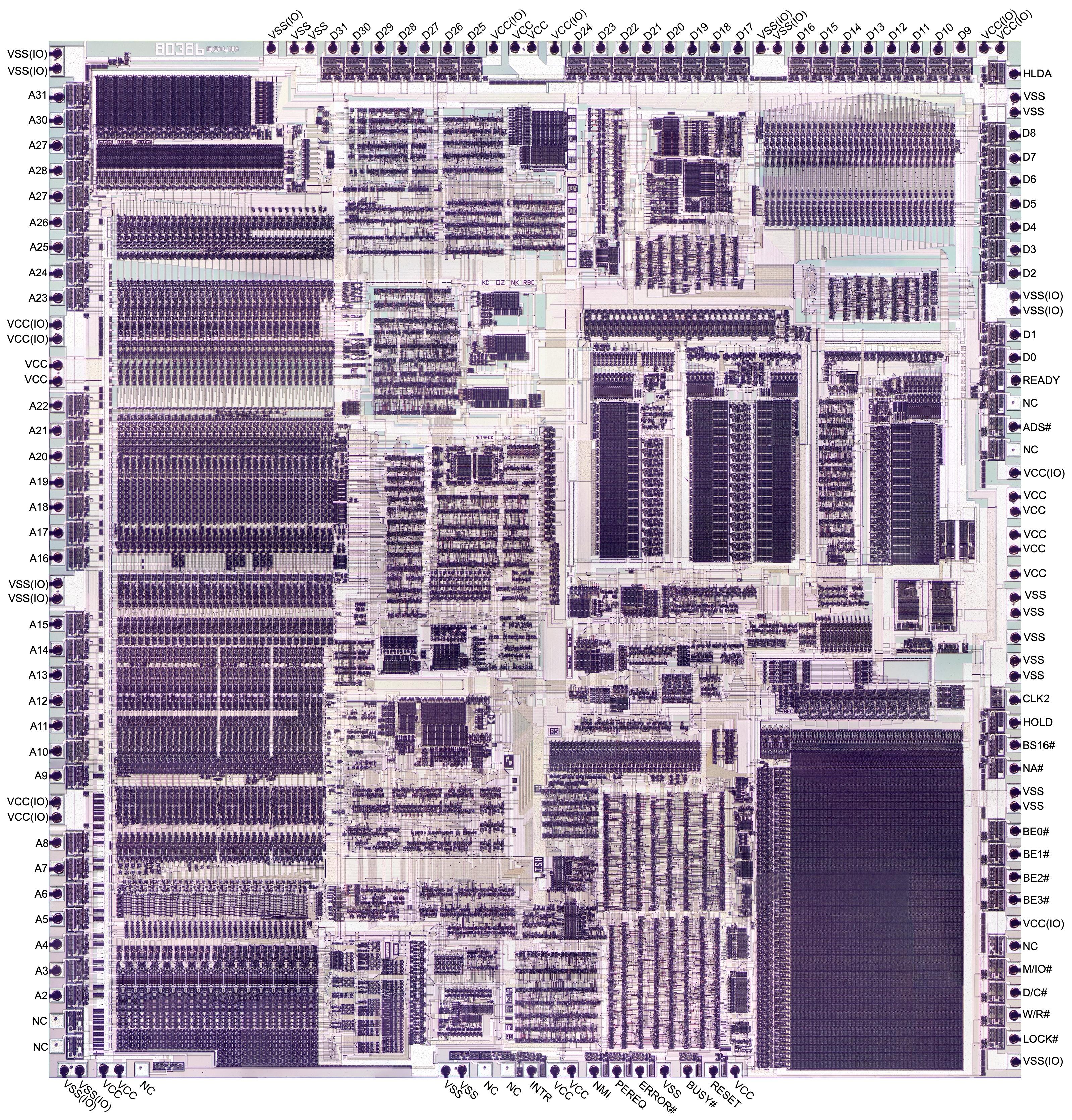
As for other features on the chip, the black circles around the border are bond wire connections that go to the chip's external pins. The chip has two metal layers, a small number by modern standards, but a jump from the single metal layer of earlier processors such as the 286. The metal appears white in larger areas, but purplish where circuitry underneath roughens its surface. For the most part, the underlying silicon and the polysilicon wiring on top are obscured by the metal layers.

Die photo of the 386 processor with standard-cell logic highlighted in red.

Die photo of the 386 processor with standard-cell logic highlighted in red.

Early processors in the 1970s were usually designed by manually laying out every transistor individually, fitting transistors together like puzzle pieces to optimize their layout. While this was tedious, it resulted in a highly dense layout. Federico Faggin, designer of the popular Z80 processor, describes finding that the last few transistors wouldn't fit, so he had to erase three weeks of work and start over. The closeup of the resulting Z80 layout below shows that each transistor has a different, complex shape, optimized to pack the transistors as tightly as possible.2

A closeup of transistors in the Zilog Z80 processor (1976). This chip is NMOS, not CMOS, which provides more layout flexibility. The metal and polysilicon layers have been removed to expose the underlying silicon. The lighter stripes over active silicon indicate where the polysilicon gates were. I think this photo is from the Visual 6502 project but I'm not sure.

A closeup of transistors in the Zilog Z80 processor (1976). This chip is NMOS, not CMOS, which provides more layout flexibility. The metal and polysilicon layers have been removed to expose the underlying silicon. The lighter stripes over active silicon indicate where the polysilicon gates were. I think this photo is from the Visual 6502 project but I'm not sure.

Standard-cell logic is an alternative that is much easier than manual layout.3 The idea is to create a standard library of blocks (cells) to implement each type of gate, flip-flop, and other low-level component. To use a particular circuit, instead of arranging each transistor, you use the standard design. Each cell has a fixed height but the width varies as needed, so the standard cells can be arranged in rows. For example, the die photo below three cells in a row: a latch, a high-current inverter, and a second latch. This region has 24 transistors in total with PMOS above and NMOS below. Compare the orderly arrangement of these transistors with the Z80 transistors above.

Some standard cell circuitry in the 386. I removed the metal and polysilicon to show the underlying silicon. The irregular blotches are oxide that wasn't fully removed, and can be ignored.

Some standard cell circuitry in the 386. I removed the metal and polysilicon to show the underlying silicon. The irregular blotches are oxide that wasn't fully removed, and can be ignored.

The space between rows is used as a "wiring channel" that holds the wiring between the cells. The photo below zooms out to show four rows of standard cells (the dark bands) and the wiring in between. The 386 uses three layers for this wiring: polysilicon and the upper metal layer (M2) for vertical segments and the lower metal layer (M1) for horizontal segments.

Some standard-cell logic in the 386 processor.

Some standard-cell logic in the 386 processor.

To summarize, with standard cell logic, the cells are obtained from the standard cell library as needed, defining the transistor layout and the wiring inside the cell. However, the locations of each cell (placing) need to be determined, as well as how to arrange the wiring (routing). As will be seen, placing and routing the cells can be done manually or automatically.

Use of standard cells in the 386

Fairly late in the design process, the 386 team decided to use automatic place and route for parts of the chip. By using automatic place and route, 2,254 gates (consisting of over 10,000 devices) were placed and routed in seven weeks. (These numbers are from a paper "Automatic Place and Route Used on the 80386", co-written by Pat Gelsinger, now the CEO of Intel. I refer to this paper multiple times, so I'll call it APR386 for convenience.4) Automatic place and route was not only faster, but it avoided the errors that crept in when layout was performed manually.5

The "place" part of automatic place and route consists of determining the arrangement of the standard cells into rows to minimize the distance between connected cells. Running long wires between cells wastes space on the die, since you end up with a lot of unnecessary metal wiring. But more importantly, long paths have higher resistance, slowing down the signals. Placement is a difficult optimization problem that is NP-complete. Moreover, the task was made more complicated by weighting paths by importance and electrical characteristics, classifying signals as "normal", "fast", or "critical". Paths were also weighted to encourage the use of the thicker M2 metal layer rather than the lower M1 layer.

The 386 team solved the placement problem with a program called Timberwolf, developed by a Berkeley grad student. As one member of the 386 team said, "If management had known that we were using a tool by some grad student as a key part of the methodology, they would never have let us use it." Timberwolf used a simulated annealing algorithm, based on a simulated temperature that decreased over time. The idea is to randomly move cells around, trying to find better positions, but gradually tighten up the moves as the "temperature" drops. At the end, the result is close to optimal. The purpose of the temperature is to avoid getting stuck in a local minimum by allowing "bad" changes at the beginning, but then tightening up the changes as the algorithm progresses.

Once the cells were placed in their positions, the second step was "routing", generating the layout of all the wiring. A suitable commercial router was not available in 1984, so Intel developed its own. As routing is a difficult problem (also NP-complete), they took an iterative heuristic approach, repeatedly routing until they found the smallest channel height that would work. (Thus, the wiring channels are different sizes as needed.) Then they checked the R-C timing of all the signals to find any signals that were too slow. Designers could boost the size of the associated drivers (using the variety of available standard cells) and try the routing again.

Brief CMOS overview

The 386 was the first processor in Intel's x86 line to be built with a technology called CMOS instead of using NMOS. Modern processors are all built from CMOS because CMOS uses much less power than NMOS. CMOS is more complicated to construct, though, because it uses two types of transistors—NMOS and PMOS—so early processors were typically NMOS. But by the mid-1980s, the advantages of switching to CMOS were compelling.

The diagram below shows how an NMOS transistor is constructed. The transistor can be considered a switch between the source and drain, controlled by the gate. The source and drain regions (green) consist of silicon doped with impurities to change its semiconductor properties, forming N+ silicon. The gate consists of a layer of polysilicon (red), separated from the silicon by a very thin insulating oxide layer. Whenever polysilicon crosses active silicon, a transistor is formed. A PMOS transistor has similar construction except it swaps the N-type and P-type silicon, consisting of P+ regions in a substrate of N silicon.

Diagram showing the structure of an NMOS transistor.

Diagram showing the structure of an NMOS transistor.

The NMOS and PMOS transistors are opposite in their construction and operation. An NMOS transistor turns on when the gate is high, while a PMOS transistor turns on when the gate is low. An NMOS transistor is best at pulling its output low, while a PMOS transistor is best at pulling its output high. In a CMOS circuit, the transistors work as a team, pulling the output high or low as needed; this is the "Complementary" in CMOS. (The behavior of MOS transistors is complicated, so this description is simplified, just enough to understand digital circuits.)

One complication is that NMOS transistors are built on P-type silicon, while PMOS transistors are built on N-type silicon. Since the silicon die itself is N silicon, the NMOS transistors need to be surrounded by a tub or well of P silicon.6 The cross-section diagram below shows how the NMOS transistor on the left is embedded in a well of P-type silicon.

Simplified structure of the CMOS circuits.

Simplified structure of the CMOS circuits.

For proper operation, the silicon that surrounds transistors needs to be connected to the appropriate voltage through "tap" contacts.7 For PMOS transistors, the substrate is connected to power through the taps, while for NMOS transistors the well region is connected to ground through the taps. The chip needs to have enough taps to keep the voltage from fluctuating too much; each standard cell typically has a positive tap and a ground tap.

The actual structure of the integrated circuit is much more three-dimensional than the diagram above, due to the thickness of the various layers. The diagram below is a more accurate cross-section. The 386 has two layers of metal: the lower metal layer (M1) in blue and the upper metal layer (M2) in purple. Polysilicon is colored red, while the insulating oxide layers are gray.

Cross-section of CHMOS III transistors. From A double layer metal CHMOS III technology, image colorized by me.

Cross-section of CHMOS III transistors. From A double layer metal CHMOS III technology, image colorized by me.

This complicated three-dimensional structure makes it harder to interpret the microscope images. Moreover, the two metal layers obscure the circuitry underneath. I have removed various layers with acids for die photos, but even so, the images are harder to interpret than those of simpler chips. If the die photos look confusing, don't be surprised.

A logic gate in CMOS is constructed from NMOS and PMOS transistors working together. The schematic below shows a NAND gate with two PMOS transistors in parallel above and two NMOS transistors in series below. If both inputs are high, the two NMOS transistors turn on, pulling the output low. If either input is low, a PMOS transistor turns on, pulling the output high. (Recall that NMOS and PMOS are opposites: a high voltage turns an NMOS transistor on while a low voltage turns a PMOS transistor on.) Thus, the CMOS circuit below produces the desired output for the NAND function.

A CMOS NAND gate.

A CMOS NAND gate.

The diagram below shows how this NAND gate is implemented in the 386 as a standard cell.9 A lot is going on in this cell, but it boils down to four transistors, as in the schematic above. The yellow region is the P-type silicon that forms the two PMOS transistors; the transistor gates are where the polysilicon (red) crosses the yellow region.8 (The middle yellow region is the drain for both transistors; there is no discrete boundary between the transistors.) Likewise, the two NMOS transistors are at the bottom, where the polysilicon (red) crosses the active silicon (green). The blue lines indicate the metal wiring for the cell. I thinned these lines to make the diagram clearer; in the actual cell, the metal lines are as thick as they can be without touching, so they cover most of the cell. The black circles are contacts, connections between the metal and the silicon or polysilicon. Finally, the well taps are the opposite type of silicon, connected to the underlying silicon well or substrate to keep it at the proper voltage.

A standard cell for NAND in the 386.

A standard cell for NAND in the 386.

Wiring to a cell's inputs and output takes place at the top or bottom of the cell, with wiring in the channels between rows of cells. The polysilicon input and output lines are thickened at the top and bottom of the cell to allow connections to the cell. The wiring between cells can be done with either polysilicon or metal. Typically the upper metal layer (M2) is used for vertical wiring, while the lower metal layer (M1) is used for horizontal runs. Since each standard cell only uses M1, vertical wiring (M2) can pass over cells. Moreover, a cell's output can also use a vertical metal wire (M2) rather than the polysilicon shown. The point is that there is a lot of flexibility in how the system can route wires between the cells. The power and ground wires (M1) are horizontal so they can run from cell to cell and a whole row can be powered from the ends.

The photo below shows this NAND cell with the metal layers removed by acid, leaving the silicon and the polysilicon. You can match the features in the photo with the diagram above. The polysilicon appears green due to thin-film effects. At the bottom, two polysilicon lines are connected to the inputs.

Die photo of the NAND standard cell with the metal layers removed. The image isn't as clear as I would like, but it was very difficult to remove the metal without destroying the polysilicon.

Die photo of the NAND standard cell with the metal layers removed. The image isn't as clear as I would like, but it was very difficult to remove the metal without destroying the polysilicon.

The photo below shows how the cell appears in the original die. The two metal layers are visible, but they hide the polysilicon and silicon underneath. The vertical metal stripes are the upper (M2) wiring while the lower metal wiring (M1) makes up the standard cell. It is hard to distinguish the two metal layers, which makes interpretation of the images difficult. Note that the metal wiring is wide, almost completely covering the cell, with small gaps between wires. The contacts are visible as dark circles. Is hard to recognize the standard cells from the bare die, as the contact pattern is the only distinguishing feature.

Die photo of the NAND standard cell showing the metal layer.

Die photo of the NAND standard cell showing the metal layer.

One of the interesting features of the 386's standard cell library is that each type of logic gate is available in multiple drive strengths. That is, cells are available with small transistors, large transistors, or multiple transistors in parallel. Because the wiring and the transistor gates have capacitance, a delay occurs when changing state. Bigger transistors produce more current, so they can switch the values on a wire faster. But there are two disadvantages to bigger transistors. First, they take up more space on the die. But more importantly, bigger transistors have bigger gates with more capacitance, so their inputs take longer to switch. (In other words, increasing the transistor size speeds up the output but slows the input, so overall performance could end up worse.) Thus, the sizes of transistors need to be carefully balanced to achieve optimum performance.10 With a variety of sizes in the standard cell library, designers can make the best choices.

The image below shows a small NAND gate. The design is the same as the one described earlier, but the transistors are much smaller. (Note that there is one row of metal contacts instead of two or three.) The transistor gates are about half as wide (measured vertically) so the NAND gate will produce about half the output current.11

Die photo of a small NAND standard cell with the metal removed.

Die photo of a small NAND standard cell with the metal removed.

Since the standard cells are all the same height, the maximum size of a transistor is limited. To provide a larger drive strength, multiple transistors can be used in parallel. The NAND gate below uses 8 transistors, four PMOS and four NMOS, providing twice as much current.

A large NAND gate as it appears on the die, with the metal removed. The left side is slightly obscured by some remaining oxide.

A large NAND gate as it appears on the die, with the metal removed. The left side is slightly obscured by some remaining oxide.

The diagram below shows the structure of the large NAND gate, essentially two NAND gates in parallel. Note that input 1 must be provided separately to both halves by the routing outside the cell. Input 2, on the other hand, only needs to be supplied to the cell once, since it is wired to both halves inside the cell.

A diagram showing the structure of the large NAND gate.

A diagram showing the structure of the large NAND gate.

Inverters are also available in a variety of drive strengths, from very small to very large, as shown below. The inverter on the left uses the smallest transistors, while the inverter on the right not only uses large transistors but is constructed from six inverters in parallel. One polysilicon input controls all the transistors.

A small inverter and a large inverter.

A small inverter and a large inverter.

A more complex standard cell is XOR. The diagram below shows an XOR cell with large drive current. (There are smaller XOR cells). As with the large NAND gate, the PMOS transistors are doubled up for more current. The multiple input connections are handled by the routing outside the cell. Since the NMOS transistors don't need to be doubled up, there is a lot of unused space in the lower part of the cell. The extra space is used for a very large tap contact, consisting of 24 contacts to ground the well.

The structure of an XOR cell with large drive current.

The structure of an XOR cell with large drive current.

XOR is a difficult gate to build with CMOS. The cell above implements it by combining a NOR gate and an AND-NOR gate, as shown below. You can verify that if both inputs are 0 or both inputs are 1, the output is forced low as desired. In the layout above, the NOR gate is on the left, while the AND-NOR gate has the AND part on the right. A metal wire down the center connects the NOR output to the AND-NOR input. The need for two sub-gates is another reason why the XOR cell is so large.

Schematic of the XOR cell.

Schematic of the XOR cell.

I'll describe one more cell, the latch, which holds one bit and is controlled by a clock signal. Latches are heavily used in the 386 whenever a signal needs to be remembered or a circuit needs to be synchronous. The 386 has multiple types of standard cell latches including latches with set or reset controls and latches with different drive strengths. Moreover, two latches can be combined to form an edge-triggered flip-flop standard cell.

The schematic below shows the basic latch circuit, the most common type in the 386. On the right, two inverters form a loop. This loop can stably hold a 0 or 1 value. On the left, a PMOS transistor and an NMOS transistor form a transmission gate. If the clock is high, both transistors will turn on and pass the input through. If the clock is low, both transistors will turn off and block the input. The trick to the latch is that one inverter is weak, producing just a small current. The consequence is that the input can overpower the inverter output, causing the inverter loop to switch to the input value. The result is that when the clock is high, the latch will pass the input value through to the output. But when the clock is low, the latch will hold its previous value. (The output is inverted with respect to the input, which is slightly inconvenient but reduces the size of the latch.)

Schematic of a latch.

Schematic of a latch.

The standard cell layout of the latch (below) is complicated, but it corresponds to the schematic. At the left are the PMOS and NMOS transistors that form the transmission gate. In the center is the weak inverter, with its output to the left. The weak transistors are in the middle; they are overlapped by a thick polysilicon region, creating a long gate that produces a low current.12 At the right is the inverter that drives the output. The layout of this circuit is clever, designed to make the latch as compact as possible. For example, the two inverters share power and ground connections. Notice how the two clock lines pass from top to bottom through gaps in the active silicon so each line only forms one transistor. Finally, the metal line in the center connects the transmission gate outputs and the weak inverter output to the other inverter's input, but asymmetrically at the top so the two inverters don't collide.

The standard cell layout of a latch.

The standard cell layout of a latch.

To summarize, I examined many (but not all) of the standard cells in the 386 and found about 70 different types of cells. These included the typical logic gates with various drive strengths: inverters, buffers, XOR, XNOR, AND-NOR, and 3- and 4-input logic gates. There are also transmission gates including ones that default high or low, as well as multiplexers built from transmission gates. I found a few cells that were surprising such as dual inverters and a combination 3-input and 2-input NAND gate. I suspect these consist of two standard cells that were merged together, since they seem too specialized to be part of a standard cell library.

The APR386 paper showed six of the standard cells in the 386 with the diagram below. The small and large inverters are the same as the ones described above, as is the NAND gate NA2B. The latch is similar to the one described above, but with larger transistors. The APR386 paper also showed a block of standard cells, which I was able to locate in the 386.13

Examples of standard cells, from APR386. The numbers are not defined but may indicate input and output capacitance. (Click for a larger version.)

Examples of standard cells, from APR386. The numbers are not defined but may indicate input and output capacitance. (Click for a larger version.)

Intel's standard cell line

Intel productized its standard cells around 1986 as a 1.5 µm library using Intel's CMOS technology (called CHMOS III).14 Although the library had over 100 cell types, it was very limited compared to the cells used inside the 386. The library included logic gates, flip-flops, and latches as well as scalable registers, counters, and adders. Most gates only came in one drive strength. Even inverters only came in "normal" and "high" drive strength. I assume these cells are the same as the ones used in the 386, but I don't have proof. The library also included larger devices such as a cell-compatible 80C51 microcontroller and PC peripheral chips such as the 8259 programmable interrupt controller and the 8254 programmable interval timer. I think these were re-implemented using standard cells.

Intel later produced a 1.0 µm library using CHMOS IV, for use "both by ASIC customers and Intel's internal chip designers." This library had a larger collection of drive strengths. The 1.0 µm library included the 80C186 and associated peripheral chips.

Layout techniques in the 386

In this section, I'll look at the active silicon regions, making the cells themselves more visible. In the photos below, I dissolved the metal and polysilicon, leaving the active silicon. (Ignore the irregular greenish shapes; these are oxide that wasn't fully removed.)

The photo below shows the silicon for three rows of standard cells using automatic place and route. You can see the wide variety of standard cell widths, but the height of the cells is constant. The transistor gates are visible as the darker vertical stripes across the silicon. You may be able to spot the latch in each row, distinguished by the long, narrow transistors of the weak inverters.

Three rows of standard cells that were automatically placed and routed.

Three rows of standard cells that were automatically placed and routed.

In the first row, the larger PMOS transistors are on top, while the smaller NMOS transistors are below. This pattern alternates from row to row, so the second row has the NMOS transistors on top and the third row has the PMOS transistors on top. The height of the wiring channel between the cells is variable, made as small as possible while fitting the wiring.

The 386 also contains regions of standard cells that were apparently manually placed and routed, as shown in the photo below. Using standard cells avoids the effort of laying out each transistor, so it is still easier than a fully custom layout. These cells are in rows, but the rows are now double rows with channels in between. The density is higher, but routing the wires becomes more challenging.

Three rows of standard cells that were manually placed and routed.

Three rows of standard cells that were manually placed and routed.

For critical circuitry such as the datapath, the layout of each transistor was optimized. The register file, for example, has a very dense layout as shown below. As you can see, the density is much higher than in the previous photos. (The three photos are at the same scale.) Transistors are packed together with very little wasted space. This makes the layout difficult since there is little room for wiring. For this particular circuit, the lower metal layer (M1) runs vertically with signals for each bit while the upper metal layer (M2) runs horizontally for power, ground, and control signals.15

Three rows of standard cells that were manually placed and routed.

Three rows of standard cells that were manually placed and routed.

The point of this is that the 386 uses a variety of different design techniques, from dense manual layout to much faster automated layout. Different techniques were used for different parts of the chip, based on how important it was to optimize. For example, circuits in the datapath were typically repeated 32 times, once for each bit, so manual effort was worthwhile. The most critical functional blocks were the microcode ROM (CROM), large PLAs, ALU, TLB (translation lookaside buffer), and the barrel shifter.16

Conclusions

Standard cell logic and automatic place and route have a long history before the 386, back to the early 1970s, so this isn't an Intel invention.17 Nonetheless, the 386 team deserves the credit for deciding to use this technology at a time when it was a risky decision. They needed to develop custom software for their placing and routing needs, so this wasn't a trivial undertaking. This choice paid off and they completed the 386 ahead of schedule. The 386 ended up being a huge success for Intel, moving the x86 architecture to 32-bits and defining the dominant computer architecture for the rest of the 20th century.

If you're interested in standard cell logic, I wrote about standard cell logic in an IBM chip. I plan to write more about the 386, so follow me on Twitter @kenshirriff or RSS for updates. I'm also on Mastodon occasionally as @kenshirriff@oldbytes.space. Thanks to Pat Gelsinger and Roxanne Koester for providing helpful papers.

Notes and references

  1. The decision to use automatic place and route is described on page 13 of the Intel 386 Microprocessor Design and Development Oral History Panel, a very interesting document on the 386 with discussion from some of the people involved in its development. 

  2. Circuits that had a high degree of regularity, such as the arithmetic/logic unit (ALU) or register storage were typically constructed by manually laying out a block to implement a bit and then repeating the block as needed. Because a circuit was repeated 32 times for the 32-bit processor, the additional effort was worthwhile. 

  3. An alternative layout technique is the gate array, which doesn't provide as much flexibility as a standard cell approach. In a gate array (sometimes called a master slice), the chip had a fixed array of transistors (and often resistors). The chip could be customized for a particular application by designing the metal layer to connect the transistors as needed. The density of the chip was usually poor, but gate arrays were much faster to design, so they were advantageous for applications that didn't need high density or produced a relatively small volume of chips. Moreover, manufacturing was much faster because the silicon wafers could be constructed in advance with the transistor array and warehoused. Putting the metal layer on top for a particular application could then be quick. Similar gate arrays used a fixed arrangement of logic gates or flip-flops, rather than transistors. Gate arrays date back to 1967

  4. The full citation for the APR386 paper is "Automatic Place and Route Used on the 80386" by Joseph Krauskopf and Pat Gelsinger, Intel Technology Journal, Spring 1986. I was unable to find it online. 

  5. Once the automatic place and route process had finished, the mask designers performed some cleanup along with compaction to squeeze out wasted space, but this was a relatively minor amount of work.

    While manual optimization has benefits, it can also be overdone. When the manufacturing process improved, the 80386 moved from a 1.5 µm process to a 1 µm process. The layout engineers took advantage of this switch to optimize the standard cell circuitry, manually squeezing out some extra space. Unfortunately, optimizing one block of a die doesn't necessarily make the die smaller, since the size is constrained by the largest blocks. The result is that the optimized 80386 has blocks of empty space at the bottom (visible as black rectangles) and the standard-cell optimization didn't provide any overall benefit. (As the Pentium Pro chief architect Robert Colwell explains, "Removing the state of Kansas does not make the perimeter of the United States any smaller.")

    Comparison of the 1.5 µm die and the 1 µm die at the same scale. Photos courtesy of Antoine Bercovici.

    Comparison of the 1.5 µm die and the 1 µm die at the same scale. Photos courtesy of Antoine Bercovici.

    At least compaction went better for the 386 than for the Pentium. Intel performed a compaction on the Pentium shortly before release, attempting to reduce the die size. The engineers shrunk the floating point divider, removing some lookup table cases that they proved were unnecessary. Unfortunately, the proof was wrong, resulting in floating point errors in a few cases. This caused the infamous Pentium FDIV bug, a problem that became highly visible to the general public. Replacing the flawed processors cost Intel 475 million dollars. And it turned out that shrinking the floating point divider had no effect on the overall die size.

    Coincidentally, early models of the 386 had an integer multiplication bug, but Intel fixed this with little cost or criticism. The 386 bug was an analog issue that only showed up unpredictably with a combination of argument values, temperature, and manufacturing conditions. 

  6. This chip is built on a substrate of N-type silicon, with wells of P-type silicon for the NMOS transistors. Chips can be built the other way around, starting with P-type silicon and putting wells of N-type silicon for the PMOS transistors. Another approach is the "twin-well" CMOS process, constructing wells for both NMOS and PMOS transistors. 

  7. The bulk silicon voltage makes the boundary between a transistor and the bulk silicon act as a reverse-biased diode, so current can't flow across the boundary. Specifically, for a PMOS transistor, the N-silicon substrate is connected to the positive supply. For an NMOS transistor, the P-silicon well is connected to ground. A P-N junction acts as a diode, with current flowing from P to N. But the substrate voltages put P at ground and N at +5, blocking any current flow. The result is that the bulk silicon can be considered an insulator, with current restricted to the N+ and P+ doped regions. If this back bias gets reversed, for example, due to power supply fluctuations, current can flow through the substrate. This can result in "latch-up", a situation where the N and P regions act as parasitic NPN and PNP transistors that latch into the "on" state. This shorts power and ground and can destroy the chip. The point is that the substrate voltages are very important for the proper operation of the chip. 

  8. I'm using the standard CMOS coloring scheme for my diagrams. I'm told that Intel uses a different color scheme internally. 

  9. The schematic below shows the physical arrangement of the transistors for the NAND gate, in case it is unclear how to get from the layout to the logic gate circuit. The power and ground lines are horizontal so power can pass from cell to cell when the cells are connected in rows. The gate's inputs and outputs are at the top and bottom of the cell, where they can be connected through the wiring channels. Even though the transistors are arranged horizontally, the PMOS transistors (top) are in parallel, while the NMOS transistors (bottom) are in series.

    Schematic of the NAND gate as it is arranged in the standard cell.

    Schematic of the NAND gate as it is arranged in the standard cell.


  10. The 1999 book Logical Effort describes a methodology for maximizing the performance of CMOS circuits by correctly sizing the transistors. 

  11. Unfortunately, the word "gate" is used for both transistor gates and logic gates, which can be confusing. 

  12. You might expect that these transistors would produce more current since they are larger than the regular transistors. The reason is that a transistor's current output is proportional to the gate width divided by the length. Thus, if you make the transistor bigger in the width direction, the current increases, but if you make the transistor bigger in the length direction, the current decreases. You can think of increasing width as acting as multiple transistors in parallel. Increasing length, on the other hand, makes a longer path for current to get from the source to the drain, weakening it. 

  13. The APR386 paper discusses the standard-cell layout in detail. It includes a plot of a block of standard-cell circuitry (below).

    A block of standard-cell circuitry from APR386.

    A block of standard-cell circuitry from APR386.

    After carefully studying the 386 die, I was able to find the location of this block of circuitry (below). The two regions match exactly; they look a bit different because the M1 metal layer (horizontal) doesn't show up in the plot above.

    The same block of standard cells on the 386 die.

    The same block of standard cells on the 386 die.


  14. Intel's CHMOS III standard cells are documented in Introduction to Intel Cell-Based Design (1988). The CHMOS IV library is discussed in Design Methodology for a 1.0µ Cell-based Library Efficiently Optimized for Speed and Area. The paper Validating an ASIC Standard Cell Library covers both libraries. 

  15. For details on the 386's register file, see my earlier article

  16. Source: "High Performance Technology Circuits and Packaging for the 80386", Jan Prak, Proceedings, ICCD Conference, Oct. 1986. 

  17. I'll provide more history on standard cells in this footnote. RCA patented a bipolar standard cell in 1971, but this was a fixed arrangement of transistors and resistors, more of a gate array than a modern standard cell. Bell Labs researched standard cell layout techniques in the early 1970s, calling them Polycells, including a 1973 paper by Brian Kernighan. By 1979 A Guide to LSI Implementation discussed the standard cell approach and it was described as well-known in this patent application. Even so, Electronics called these design methods "futuristic" in 1980.

    Standard cells became popular in the mid-1980s as faster computers and improved design software made it practical to produce semi-custom designs that used standard cells. Standard cells made it to the cover of Digital Design in August 1985, and the article inside described numerous vendors and products. Companies like Zymos and VLSI Technology (VTI) focused on standard cells. Traditional companies such as Texas Instruments, NCR, GE/RCA, Fairchild, Harris, ITT, and Thomson introduced lines of standard cell products in the mid-1980s.  

Two interesting XOR circuits inside the Intel 386 processor

16 December 2023 at 06:36

Intel's 386 processor (1985) was an important advance in the x86 architecture, not only moving to a 32-bit processor but also switching to a CMOS implementation. I've been reverse-engineering parts of the 386 chip and came across two interesting and completely different circuits that the 386 uses to implement an XOR gate: one uses standard-cell logic while the other uses pass-transistor logic. In this article, I take a look at those circuits.

The die of the 386. Click this image (or any other) for a larger version.

The die of the 386. Click this image (or any other) for a larger version.

The die photo above shows the two metal layers of the 386 die. The polysilicon and silicon layers underneath are mostly hidden by the metal. The black dots around the edges are the bond wires connecting the die to the external pins. The 386 is a complicated chip with 285,000 transistor sites. I've labeled the main functional blocks. The datapath in the lower left does the actual computations, controlled by the microcode ROM in the lower right.

Despite the complexity of the 386, if you zoom in enough, you can see individual XOR gates. The red rectangle at the top (below) is a shift register for the chip's self-test. Zooming in again shows the silicon for an XOR gate implemented with pass transistors. The purple outlines reveal active silicon regions, while the stripes are transistor gates. The yellow rectangle zooms in on part of the standard-cell logic that controls the prefetch queue. The closeup shows the silicon for an XOR gate implemented with two logic gates. Counting the stripes shows that the first XOR gate is implemented with 8 transistors while the second uses 10 transistors. I'll explain below how these transistors are connected to form the XOR gates.

The die of the 386, zooming in on two XOR gates.

The die of the 386, zooming in on two XOR gates.

A brief introduction to CMOS

CMOS circuits are used in almost all modern processors. These circuits are built from two types of transistors: NMOS and PMOS. These transistors can be viewed as switches between the source and drain controlled by the gate. A high voltage on the gate of an NMOS transistor turns the transistor on, while a low voltage on the gate of a PMOS transistor turns the transistor on. An NMOS transistor is good at pulling the output low, while a PMOS transistor is good at pulling the output high. Thus, NMOS and PMOS transistors are opposites in many ways; they are complementary, which is the "C" in CMOS.

Structure of a MOS transistor. Although the transistor's name represents the Metal-Oxide-Semiconductor layers, modern MOS transistors typically use polysilicon instead of metal for the gate.

Structure of a MOS transistor. Although the transistor's name represents the Metal-Oxide-Semiconductor layers, modern MOS transistors typically use polysilicon instead of metal for the gate.

In a CMOS circuit, the NMOS and PMOS transistors work together, with the NMOS transistors pulling the output low as needed while the PMOS transistors pull the output high. By arranging the transistors in different ways, different logic gates can be created. The diagram below shows a NAND gate constructed from two PMOS transistors (top) and two NMOS transistors (bottom). If both inputs are high, the NMOS transistors turn on and pull the output low. But if either input is low, a PMOS transistor will pull the output high. Thus, the circuit below implements a NAND gate.

A NAND gate implemented in CMOS.

A NAND gate implemented in CMOS.

Notice that NMOS and PMOS transistors have an inherent inversion: a high input produces a low (for NMOS) or a low input produces a high (for PMOS). Thus, it is straightforward to produce logic circuits such as an inverter, NAND gate, NOR gate, or an AND-OR-INVERT gate. However, producing an XOR (exclusive-or) gate doesn't work with this approach: an XOR gate produces a 1 if either input is high, but not both.1 The XNOR (exclusive-NOR) gate, the complement of XOR, also has this problem. As a result, chips often have creative implementations of XOR gates.

The standard-cell two-gate XOR circuit

Parts of the 386 were implemented with standard-cell logic. The idea of standard-cell logic is to build circuitry out of standardized building blocks that can be wired by a computer program. In earlier processors such as the 8086, each transistor was carefully positioned by hand to create a chip layout that was as dense as possible. This was a tedious, error-prone process since the transistors were fit together like puzzle pieces. Standard-cell logic is more like building with LEGO. Each gate is implemented as a standardized block and the blocks are arranged in rows, as shown below. The space between the rows holds the wiring that connects the blocks.

Some rows of standard-cell logic in the 386 processor. This is part of the segment descriptor control circuitry.

Some rows of standard-cell logic in the 386 processor. This is part of the segment descriptor control circuitry.

The advantage of standard-cell logic is that it is much faster to create a design since the process can be automated. The engineer described the circuit in terms of the logic gates and their connections. A computer algorithm placed the blocks so related blocks are near each other. An algorithm then routed the circuit, creating the wiring between the blocks. These "place and route" algorithms are challenging since it is an extremely difficult optimization problem, determining the best locations for the blocks and how to pack the wiring as densely as possible. At the time, the algorithm took a day on a powerful IBM mainframe to compute the layout. Nonetheless, the automated process was much faster than manual layout, cutting weeks off the development time for the 386. The downside is that the automated layout is less dense than manually optimized layout, with a lot more wasted space. (As you can see in the photo above, the density is low in the wiring channels.) For this reason, the 386 used manual layout for circuits where a dense layout was important, such as the datapath.

In the 386, the standard-cell XOR gate is built by combining a NOR gate with an AND-NOR gate as shown below.2 (Although AND-NOR looks complicated, it is implemented as a single gate in CMOS.) You can verify that if both inputs are 0, the NOR gate forces the output low, while if both inputs are 1, the AND gate forces the output low, providing the XOR functionality.

Schematic of an XOR circuit.

Schematic of an XOR circuit.

The photo below shows the layout of this XOR gate as a standard cell. I have removed the metal and polysilicon layers to show the underlying silicon. The outlined regions are the active silicon, with PMOS above and NMOS below. The stripes are the transistor gates, normally covered by polysilicon wires. Notice that neighboring transistors are connected by shared silicon; there is no demarcation between the source of one transistor and the drain of the next.

The silicon implementing the XOR standard cell. This image is rotated 180° from the layout on the die to put PMOS at the top.

The silicon implementing the XOR standard cell. This image is rotated 180° from the layout on the die to put PMOS at the top.

The schematic below corresponds to the silicon above. Transistors a, b, c, and d implement the first NOR gate. Transistors g, h, i, and j implement the AND part of the AND-NOR gate. Transistors e and f implement the NOR input of the AND-NOR gate, fed from the first NOR gate. The standard cell library is designed so all the cells are the same height with a power rail at the top and a ground rail at the bottom. This allows the cells to "snap together" in rows. The wiring inside the cell is implemented in polysilicon and the lower metal layer (M1), while the wiring between cells uses the upper metal layer (M2) for vertical connections and lower metal (M1) for horizontal connections. This strategy allows vertical wires to pass over the cells without interfering with the cell's wiring.

Transistor layout in the XOR standard cell.

Transistor layout in the XOR standard cell.

One important factor in a chip such as the 386 is optimizing the sizes of transistors. If a transistor is too small, it will take too much time to switch its output line, reducing performance. But if a transistor is too large, it will waste power as well as slowing down the circuit that is driving it. Thus, the standard-cell library for the 386 includes several XOR gates of various sizes. The diagram below shows a considerably larger XOR standard cell. The cell is the same height as the previous XOR (as required by the standard cell layout), but it is much wider and the transistors inside the cell are taller. Moreover, the PMOS side uses pairs of transistors to double the current capacity. (NMOS has better performance than PMOS so doesn't require doubling of the transistors.) Thus, there are 10 PMOS transistors and 5 NMOS transistors in this XOR cell.

A large XOR standard cell. This cell is also rotated from the die layout.

A large XOR standard cell. This cell is also rotated from the die layout.

The pass transistor circuit

Some parts of the 386 implement XOR gates completely differently, using pass transistor logic. The idea of pass transistor logic is to use transistors as switches that pass inputs through to the output, rather than using transistors as switches to pull the output high or low. The pass transistor XOR circuit uses 8 transistors, compared with 10 for the previous circuit.3

The die photo below shows a pass-transistor XOR circuit, highlighted in red. Note that the surrounding circuitry is irregular and much more tightly packed than the standard-cell circuitry. This circuit was laid out manually producing an optimized layout compared to standard cells. It has four PMOS transistors at the top and four NMOS transistors at the bottom.

The pass-transistor XOR circuit on the die. The green regions are oxide that was not completely removed causing thin-film interference.

The pass-transistor XOR circuit on the die. The green regions are oxide that was not completely removed causing thin-film interference.

The schematic below shows the heart of the circuit, computing the exclusive-NOR (XNOR) of X and Y with four pass transistors. To understand the circuit, consider the four input cases for X and Y. If X and Y are both 0, PMOS transistor a will turn on (because Y is low), passing 1 to the XNOR output. (X is the complemented value of the X input.) If X and Y are both 1, PMOS transistor b will turn on (because X is low), passing 1. If X and Y are 1 and 0 respectively, NMOS transistor c will turn on (because X is high), passing 0. If X and Y are 0 and 1 respectively, transistor d will turn on (because Y is high), passing 0. Thus, the four transistors implement the XNOR function, with a 1 output if both inputs are the same.

Partial implementation of XNOR with four pass transistors.

Partial implementation of XNOR with four pass transistors.

To make an XOR gate out of this requires two additional inverters. The first inverter produces X from X. The second inverter generates the XOR output by inverting the XNOR output. The output inverter also has the important function of buffering the output since the pass transistor output is weaker than the inputs. Since each inverter takes two transistors, the complete XOR circuit uses 8 transistors. The schematic below shows the full circuit. The i1 transistors implement the input inverter and the i2 transistors implement the output inverter. The layout of this schematic matches the earlier die photo.5

Implementation of NOR with eight pass transistors.

Implementation of NOR with eight pass transistors.

Conclusions

An XOR gate may seem like a trivial circuit, but there is more going on than you might expect. I think it is interesting that there isn't a single solution for implementing XOR; even inside a single chip, multiple approaches can be used. (If you're interested in XOR circuits, I also looked at the XOR circuit in the Z80.) It's also reassuring to see that even for a complex chip such as the 386, the circuitry can be broken down into logic gates and then understood at the transistor level.

I plan to write more about the 386, so follow me on Twitter @kenshirriff or RSS for updates. I'm also on Mastodon occasionally as @kenshirriff@oldbytes.space.

Notes and references

  1. You can't create an AND or OR gate directly from CMOS either, but this isn't usually a problem. One approach is to create a NAND (or NOR) gate and then follow it with an inverter, but this requires an "extra" inverter. However, the inverter can often be eliminated by flipping the action of the next gate (using De Morgan's laws). For example, if you have AND gates feeding into an OR gate, you can change the circuit to use NAND gates feeding into a NAND gate, eliminating the inverters. Unfortunately, flipping the logic levels doesn't help with XOR gates, since XNOR is just as hard to produce. 

  2. The 386 also uses XNOR standard-cell gates. These are implemented with the "opposite" circuit from XOR, swapping the AND and OR gates:

    Schematic of an XNOR circuit.

    Schematic of an XNOR circuit.


  3. I'm not sure why some circuits in the 386 use standard logic for XOR while other circuits use pass transistor logic. I suspect that the standard XOR is used when the XOR gate is part of a standard-cell logic circuit, while the pass transistor XOR is used in hand-optimized circuits. There may also be performance advantages to one over the other. 

  4. The first inverter can be omitted in the pass transistor XOR circuit if the inverted input happens to be available. In particular, if multiple XOR gates use the same input, one inverter can provide the inverted input to all of them, reducing the per-gate transistor count. 

  5. The pass transistor XOR circuit uses different layouts in different parts of the 386, probably because hand layout allows it to be optimized. For instance, the instruction decoder uses the XOR circuit below. This circuit has four PMOS transistors on the left and four NMOS transistors on the right.

    An XOR circuit from the instruction decoder.

    An XOR circuit from the instruction decoder.

    The schematic shows the wiring of this circuit. Although the circuit is electrically the same as the previous pass-transistor circuit, the layout is different. In the previous circuit, several of the transistors were connected through their silicon, while this circuit has all the transistors separated and arranged in columns.

    Schematic of the XOR circuit from the instruction decoder.

    Schematic of the XOR circuit from the instruction decoder.


Reverse engineering the barrel shifter circuit on the Intel 386 processor die

6 December 2023 at 17:12

The Intel 386 processor (1985) was a large step from the 286 processor, moving x86 to a 32-bit architecture. The 386 also dramatically improved the performance of shift and rotate operations by adding a "barrel shifter", a circuit that can shift by multiple bits in one step. The die photo below shows the 386's barrel shifter, highlighted in the lower left and taking up a substantial part of the die.

The 386 die with the main functional blocks labeled. Click this image (or any other) for a larger version.)

The 386 die with the main functional blocks labeled. Click this image (or any other) for a larger version.)

Shifting is a useful operation for computers, moving a binary value left or right by one or more bits. Shift instructions can be used for multiplying or dividing by powers of two, and as part of more general multiplication or division. Shifting is also useful for extracting bit fields, aligning bitmap graphics, and many other tasks.1

Barrel shifters require a significant amount of circuitry. A common approach is to use a crossbar, a matrix of switches that can connect any input to any output. By closing switches along a desired diagonal, the input bits are shifted. The diagram below illustrates a 4-bit crossbar barrel shifter with inputs X (vertical) and outputs Y (horizontal). At each point in the grid, a switch (triangle) connects a vertical input line to a horizontal output line. Energizing the blue control line, for instance, passes the value through unchanged (X0 to Y0 and so forth). Energizing the green control line rotates the value by one bit position (X0 to Y1 and so forth, with X3 wrapping around to X0). Similarly, the circuit can shift by 2 or 3 bits. The shift control lines select the amount of shift. These lines run diagonally, which will be important later.

A four-bit crossbar switch with inputs X and outputs Y. Image by Cmglee, CC BY-SA 3.0.

A four-bit crossbar switch with inputs X and outputs Y. Image by Cmglee, CC BY-SA 3.0.

The main problem with a crossbar barrel shifter is that it takes a lot of hardware. The 386's barrel shifter has a 64-bit input and a 32-bit output,2 so the approach above would require 2048 switches (64×32). For this reason, the 386 uses a hybrid approach, as shown below. It has a 32×8 crossbar that can shift by 0 to 28 bits, but only in multiples of 4, making the circuit much smaller. The output from the crossbar goes to a second circuit that can shift by 0, 1, 2, or 3 bits. The combined circuitry supports an arbitrary shift, but requires less hardware than a complete crossbar. The inputs to the barrel shifter are two 32-bit values from the processor's register file, stored in latches for use by the shifter.

Block diagram of the barrel shifter circuit.

Block diagram of the barrel shifter circuit.

The figure below shows how the shifter circuitry appears on the die; this image shows the two metal layers on the die's surface. The inputs from the register file are at the bottom, for bits 31 through 0. Above that, the input latches hold the two 32-bit inputs for the shifter. In the middle is the heart of the shift circuit, the crossbar matrix. This takes the two 32-bit inputs and produces a 32-bit output. The matrix is controlled by sloping polysilicon lines, driven by control circuitry on the right. The matrix output goes to the circuit that applies a shift of 0 to 3 positions. Finally, the outputs exit at the top, where they go to other parts of the CPU. The shifter performs right shifts, but as will be explained below, the same circuit is used for the left shift instructions.

The barrel shifter circuitry as it appears on the die. I have cut out repetitive circuitry from the middle because the complete image is too wide to display clearly.

The barrel shifter circuitry as it appears on the die. I have cut out repetitive circuitry from the middle because the complete image is too wide to display clearly.

The barrel shifter crossbar matrix

In this section, I'll describe the matrix part of the barrel shifter circuit. The shift matrix takes 32-bit values a and b. Value b is shifted to the right, with bits from a filling in at the left, producing a 32-bit output. (As will be explained below, the output is actually 37 bits due to some complications, but ignore that for now.) The shift count is a multiple of 4 from 0 to 28.

The diagram below illustrates the structure of the shift matrix. The two 32-bit inputs are provided at the bottom, interleaved, and run vertically. The 32 output lines run horizontally. The 8 control lines run diagonally, activating the switches (black dots) to connect inputs and outputs. (For simplicity, only 3 control lines are shown.) For a shift of 0, control line 0 (red) is selected and the output is b31b30...b1b0. (You can verify this by matching up inputs to outputs through the dots along the red line.)

Diagram of the shift matrix, showing three of the shift control lines.

Diagram of the shift matrix, showing three of the shift control lines.

For a shift right of 4, the cyan control line is activated. It can be seen that the output in this case is a3a2a1a0b31b30...b5b4, shifting b to the right 4 bits and filling in four bits from a as desired. For a shift of 28, the purple control line is activated, producing the output a27...a0b31...b28. Note that the control lines are spaced four bits apart, which is why the matrix only shifts by a multiple of 4. Another important feature is that below the red diagonal, the b inputs are connected to the output, while above the diagonal, the a inputs are connected to the output. (In other words, the black dots are shifted to the right above the diagonal.) This implements the 64-bit support, taking bits from a or b as appropriate.

Looking at the implementation on the die, the vertical wires use the lower metal layer (metal 1) while the horizontal wires use the upper metal layer (metal 2), so the wires don't intersect. NMOS transistors are used as the switches to connect inputs and outputs.4 The transistors are controlled by diagonal wires constructed of polysilicon that form the transistor gates. When a particular polysilicon wire is energized, it turns on the transistors along a diagonal line, connecting those inputs and outputs.

The image below shows the left side of the matrix.5 The polysilicon control lines are the green horizontal lines stepping down to the right. These control the transistors, which appear as columns of blue-gray squares next to the polysilicon lines. The metal layers have been removed; the position of the lower metal 1 layer is visible in the vertical bluish lines.

The left side of the matrix as it appears on the die.

The left side of the matrix as it appears on the die.

The diagram below shows four of these transistors in the shifter matrix. There are four circuitry layers involved. The underlying silicon is pinkish gray; the active regions are the squares with darker borders. Next is the polysilicon (green), which forms the control lines and the transistor gates. The lower metal layer (metal 1) forms the blue vertical lines that connect to the transistors.3 The upper metal layer (metal 2) forms the horizontal bit output lines. Finally, the small black dots are the vias that connect metal 1 and metal 2. (The well taps are silicon regions connected to ground to prevent latch-up.)

Four transistors in the shifter matrix. The polysilicon and metal lines have been drawn in.

Four transistors in the shifter matrix. The polysilicon and metal lines have been drawn in.

To see how this works, suppose the upper polysilicon line is activated, turning on the top two transistors. The two vertical bit-in lines (blue) will be connected through the transistors to the top two bit out lines (purple), by way of the short light blue metal segments and the via (black dot). However, if the lower polysilicon line is activated, the bottom two transistors will be turned on. This will connect the bit-in lines to the fifth and sixth bit-out lines, four lines down from the previous ones. Thus, successive polysilicon lines shift the connections down by four lines at a time, so the shifts change in steps of 4 bit positions.

As mentioned earlier, to support the 64-bit input, the transistors below the diagonal are connected to b input while the transistors above the diagonal are connected to the a input. The photo below shows the physical implementation: the four upper transistors are shifted to the right by one wire width, so they connect to vertical a wires, while the four lower transistors are connected to b wires. (The metal wires were removed for this photo to show the transistors.)

This photo of the underlying silicon shows eight transistors. The top four transistors are shifted one position to the right. the irregular lines are remnants of other layers that I couldn't completely remove from the die.

This photo of the underlying silicon shows eight transistors. The top four transistors are shifted one position to the right. the irregular lines are remnants of other layers that I couldn't completely remove from the die.

In the matrix, the output signals run horizontally. In order for signals to exit the shifter from the top of the matrix, each horizontal output wire is connected to a vertical output wire. Meanwhile, other processor signals (such as the register write data) must also pass vertically through the shifter region. The result is a complicated layout, packing everything together as tightly as possible.

The precharge/keepers

At the left and the right of the barrel shifter, repeated blocks of circuitry are visible. These blocks contain precharge and keeper circuits to hold the value on one of the lines. During the first clock phase, each horizontal bit line is precharged to +5 volts. Next, the matrix is activated and horizontal lines may be pulled low. If the line is not pulled low, the inverter and PMOS transistor will continuously pull the line high. The inverter and transistor can be viewed as a bus keeper, essentially a weak latch to hold the line in the 1 state. The keeper uses relatively weak transistors, so the line can be pulled low when the barrel shifter is activated. The purpose of the keeper is to ensure that the line doesn't drift into a state between 0 and 1. This is a bad situation with CMOS circuitry, since the pull-up and pull-down transistors could both turn on, yielding a short circuit.

The precharge/keeper circuit

The precharge/keeper circuit

The motivation behind this design is that implementing the matrix with "real" CMOS would require twice as many transistors. By implementing the matrix with NMOS transistors only, the size is reduced. In a standard NMOS implementation, pull-up transistors would continuously pull the lines high, but this results in fairly high power consumption. Instead, the precharge circuit pulls the line high at the start. But this results in dynamic logic, dependent on the capacitance of the circuit to hold the charge. To avoid the charge leaking away, the keeper circuit keeps the line high until it is pulled low. Thus, this circuit minimizes the area of the matrix as well as minimizing power consumption.

There are 37 keepers in total for the 37 output lines from the matrix.6 (The extra 5 lines will be explained below.) The photo below shows one block of three keepers; the metal has been removed to show the silicon transistors and some of the polysilicon (green).

One block of keeper circuitry, to the right of the shift matrix. This block has 12 transistors, supporting three bits.

One block of keeper circuitry, to the right of the shift matrix. This block has 12 transistors, supporting three bits.

The register latches

At the bottom of the shift circuit, two latches hold the two 32-bit input values. The 386 has multi-ported registers, so it can access two registers and write a third register at the same time. This allows the shift circuit to load both values at the same time. I believe that a value can also come from the 386's constant ROM, which is useful for providing 0, 1, or all-ones to the shifter.

The schematic below shows the register latches for one bit of the shifter. Starting at the bottom are the two inputs from the register file (one appears to be inverted for no good reason). Each input is stored in a latch, using the standard 386 latch circuit.7 The latched input is gated by the clock and then goes through multiplexers allowing either value to be used as either input to the shifter. (The shifter takes two 32-bit inputs and this multiplexer allows the inputs to be swapped to the other sides of the shifter.) A second latch stage holds the values for the output; this latch is cleared during the first clock phase and holds the desired value during the second clock phase.

Circuit for one bit of the register latch.

Circuit for one bit of the register latch.

The die photo below shows the register latch circuit, contrasting the metal layers (left) with the silicon layer (right). The dark spots in the metal image are vias between the metal layers or connections to the underlying silicon or polysilicon. The metal layer is very dense with vertical wiring in the lower metal 1 layer and horizontal wiring in the upper metal 2 layer. The density of the chip seems to be constrained by the metal wiring more than the density of the transistors.

One of the register latch circuits.

One of the register latch circuits.

The 0-3 shifter

The shift matrix can only shift in steps of 4 bits. To support other shifts, a circuit at the top of the shifter provides a shift of 0 to 3 bits. In conjunction, these circuits permit a shift by an arbitrary amount.8 The schematic below shows the circuit. A bit enters at the bottom. The first shift stage passes the bit through, or sends it one bit position to the right. The second stage passes the bit through, or sends it two bit positions to the right. Thus, depending on the control lines, each bit can be shifted by 0 to 3 positions to the right. At the top, a transistor pulls the circuit low to initialize it; the NOR gate at the bottom does the same. A keeper transistor holds the circuit low until a data bit pulls it high.

One bit of the 0-3 shifter circuit.

One bit of the 0-3 shifter circuit.

The diagram below shows the silicon implementation corresponding to two copies of the schematic above. The shifters are implemented in pairs to slightly optimize the layout. In particular, the two NOR gates are mirrored so the power connection can be shared. This is a small optimization, but it illustrates that the 386 designers put a lot of work into making the layout dense.

Two bits of the 0-3 shifter circuit as it appears on the die.

Two bits of the 0-3 shifter circuit as it appears on the die.

Complications

As is usually the case with x86, there are a few complications. One complication is that the shift matrix has 37 outputs, rather than the expected 32. There are two reasons behind this. First, the upper shifter will shift right by up to 3 positions, so it needs 3 extra bits. Thus, the matrix needs to output bits 0 through 34 so three bits can be discarded. Second, shift instructions usually produce a carry bit from the last bit shifted out of the word. To support this, the shift matrix provides an extra bit at both ends for use as the carry. The result is that the matrix produces 37 outputs, which can be viewed as bits -1 through 35.

Another complication is that the x86 instruction set supports shifts on bytes and 16-bit words as well as 32-bit words. If you put two 8-bit bytes into the shifter, there will be 24 unused bits in between, posing a problem for the shifter. The solution is that some of the diagonal control lines in the matrix are split on byte and word boundaries, allowing an 8- or 16-bit value to be shifted independently. For example, you can perform a 4-bit right shift on the right-hand byte, and a 28-bit right shift on the left-hand byte. This brings the two bytes together in the result, yielding the desired 4-bit right shift. As a result, there are 18 diagonal control lines in the shifter (if I counted correctly), rather than the expected 8 control lines. This makes the circuitry to drive the control lines more complicated, as it must generate different signals depending on the size of the operand.

The control circuitry

The control circuitry at the right of the shifter drives the diagonal polysilicon lines in the matrix, selecting the desired shift. It also generates control signals for the 0-3 shifter, selecting a shift-by-1 or shift-by-2 as necessary. This circuitry operates under the control of the microcode, which tells it when to shift. It gets the shift amount from the instruction or the CL register and generates the appropriate control signals.

The distribution of control signals is more complex than you might expect. If possible, the polysilicon diagonals are connected on the right of the matrix to the control circuitry, providing a direct connection. However, many of the diagonals do not extend all the way to the right, either because they start on the left or because they are segmented for 8- or 16-bit values. Some of these signals are transmitted through polysilicon lines that run underneath the matrix. Others are transmitted through horizontal metal lines that run through the register latches. (These latches don't use many horizontal lines, so there is available space to route other signals.) These signals then ascend through the matrix at various points to connect with the polysilicon lines. This shows that the routing of this circuitry is carefully optimized to make it as compact as possible. Moreover, these "extra" lines disrupt the layout; the matrix is almost a regular pattern, but it has small irregularities throughout.

Implementing x86 shifts and rotates with the barrel shifter

The x86 has a variety of shift and rotate instructions.9 It is interesting to consider how they are implemented using the barrel shifter, since it is not always obvious. In this section, I'll discuss the instructions supported by the 386.

One important principle is that even though the circuitry shifts to the right, by changing the inputs this can achieve a shift to the left. To make this concrete, consider two input words a and b, with the shifter extracting the portion in red below. (I'll use 8-bit examples instead of 32-bit here and below to keep the size manageable.) The circuit shifts b to the right five bits, inserting bits from a at the left. Alternatively, the result can be viewed as shifting a to the left three bits, inserting bits from b at the right. Thus, the same result can be viewed as a right shift of b or a left shift of a. This holds in general, with a 32-bit right shift by N bits equivalent to a left shift by 32-N bits, depending on which word10 you focus on.

a7a6a5a4a3a2a1a0b7b6b5b4b3b2b1b0

Double shifts

The double-shift instructions (Shift Left Double (SHLD) and Shift Right Double (SHRD)) were new in the 386, shifting two 32-bit values to produce a 32-bit result. The last bit shifted out goes into the carry flag (CF). These instructions map directly onto the behavior of the barrel shifter, so I'll start with them.

Actions of the double shift instructions.

Actions of the double shift instructions.

The examples below show how the shifter implements the SHLD and SHRD instructions; the shifter output is highlighted in red. (These examples use an 8-bit source (s) and destination (d) to keep them manageable.) In either case, 3 bits of the source are shifted into the destination; shifting left or right is just a matter of whether the destination is on the left or right.

SHLD 3: ddddddddssssssss

SHRD 3: ssssssssdddddddd

Shifts

The basic shift instructions are probably the simplest. Shift Arithmetic Left (SAL) and Shift Logical Left (SHL) are synonyms, shifting the destination to the left and filling with zeroes. This can be accomplished by performing a shift with the word on the left and zeroes on the right. Shift Logical Right (SHR) is the opposite, shifting to the right and filling with zeros. This can be accomplished by putting the word on the right and zeroes on the left. Shift Arithmetic Right (SAR) is a bit different. It fills with the sign bit, the top bit. The purpose of this is to shift a signed number while preserving its sign. It can be implemented by putting all zeroes or all ones on the left, depending on the sign bit. Thus, the shift instructions map nicely onto the barrel shifter.

Actions of the shift instructions.

Actions of the shift instructions.

The 8-bit examples below show how the shifter accomplishes the SHL, SHR, and SAR instructions. The destination value d is loaded into one half of the shifter. For SAR, the value's sign bit s is loaded into the other half of the shifter, while the other instructions load 0 into the other half of the shifter. The red box shows the output from the shifter, selected from the input.

SHL 3: dddddddd00000000

SHR 3: 00000000dddddddd

SAR 3: ssssssssdddddddd

Rotates

Unlike the shift instructions, the rotate instructions preserve all the bits. As bits shift off one end, they fill in the other end, so the bit sequence rotates. A rotate left or right is implemented by putting the same word on the left and right.

Actions of the rotate instructions.

Actions of the rotate instructions.

The shifter implements rotates as shown below, using the destination value as both shifter inputs. A left shift by N bits is implemented by shifting right by 32-N bits.

ROL 3: d7d6d5d4d3d2d1d0d7d6d5d4d3d2d1d0

ROR 3: d7d6d5d4d3d2d1d0d7d6d5d4d3d2d1d0

Rotates through carry

The rotate through carry instructions perform 33-bit rotates, rotating the value through the carry bit. You might wonder how the barrel shifter can perform a 33-bit rotate, and the answer is that it can't. Instead, the instruction takes multiple steps. If you look at the instruction timings, the other shifts and rotates take three clock cycles. Rotating through the carry, however, takes nine clock cycles, performing multiple steps under the control of the microcode.

Actions of the rotate through carry instructions.

Actions of the rotate through carry instructions.

Without looking at the microcode, I can only speculate how it takes place. One sequence would be to get the top bits by putting zeroes in the right 32 bits and shifting. Next, get the bottom bits by putting the carry bit in the left 32 bits and shifting one bit more. (That is, set the left 32-bit input to either the constant 0 or 1, depending on the carry.) Finally, the result can be generated by ORing the two shift values together. The example below shows how an RCL 3 could be implemented. In the second step, the carry value C is loaded into the left side of the shifter, so it can get into the result. Note that bit d5 ends up in the carry bit, rather than the result. The RCR instruction would be similar, but adjusting the shift parameters accordingly.

First shift: d7d6d5d4d3d2d1d000000000

Second shift: 0000000Cd7d6d5d4d3d2d1d0

Result from OR: d4d3d2d1d0Cd7d6

Conclusions

The shifter circuit illustrates how the rapidly increasing transistor counts in the 1980s allowed new features. Programming languages make it easy to shift numbers with an expression such as a>>5. But it takes a lot of hardware in the processor to perform these shifts efficiently. The additional hardware of the 386's barrel shifter dramaticallly improved shift performance for shifts and rotates compared to earlier x86 processors. I estimate that the barrel shifter requires about 2000 transistors, about half the number of the entire 6502 processor (1975). But by 1985, putting 2000 transistors into a feature was practical. (In total, the 386 contains 285,000 transistors, a trivial number now, but a large number for the time.)

I plan to write more about the 386, so follow me on Twitter @kenshirriff or RSS for updates. I'm also on Mastodon occasionally as @kenshirriff@oldbytes.space.

Notes and references

  1. The earliest reference for a barrel shifter is often given as "A barrel switch design", Computer Design, 1972, but the idea of a barrel shifter goes back to 1964 at least. (The "barrel switch" name presumably comes from a physical barrel switch, a cylindrical multi-position switch such as a car ignition.) The CDC 6600 supercomputer (1964) had a 6-stage shifter able to shift up to 63 positions in one cycle (details); it was called a "parallel shifting network" rather than a "barrel shifter". A Burroughs patent filed in 1965 describes a barrel switch "capable of performing logical switching operations in a single time involving any amount of binary information," so the technology is older.

    Early microprocessors shifted by one bit position at a time. Although the Intel 8086 provided instructions to shift by multiple bits at a time, this was implemented internally by a microcode loop, so the more bits you shifted, the longer the instruction took, four clock cycles per bit. Shifting on the 286 was faster, taking one additional cycle for each bit position shifted. The first ARM processor (ARM1, 1985) included a 32-bit barrel shifter. It was considerably simpler than the 386's design, following ARM's RISC philosophy. 

  2. The 386 Hardware Reference Manual states that the 386 contains a 64-bit barrel shifter. I find this description a bit inaccurate, since the output is only 32 bits, so the barrel shifter is much simpler than a full 64-bit barrel shifter. 

  3. The 386 has two layers of metal. The vertical lines are in the lower layer of metal (metal 1) while the horizontal lines are in the upper layer of metal (metal 2). Transistors can only connect to lower metal, so the connection between the horizontal line and the transistor uses a short piece of lower metal to bridge the layers. 

  4. Each row of the matrix can be considered a multiplexer with 8 inputs, implemented by 8 pass transistors. One of the eight transistors is activated, passing that input to the output. 

  5. The image below shows the full shift matrix. Click the image for a much larger view.

    The matrix with the metal layer removed.

    The matrix with the metal layer removed.


  6. The keepers are arranged with 6 blocks of three on the left and 6 blocks of 3 on the right, plus an additional one at the bottom right. 

  7. The standard latch in the 386 consists of two cross-coupled inverters forming a static circuit to hold a bit. The input goes through a transmission gate (back-to-back NMOS and PMOS transistors) to the inverters. One inverter is weak, so it can be overpowered by the input. The 8086, in contrast, uses dynamic latches that depend on the gate capacitance to hold a bit. 

  8. Some shifters take the idea of combining shift circuits to the extreme. If you combine a shift-by-one circuit, a shift-by-two circuit, a shift-by-four circuit, and so forth, you end up with a logarithmic shifter: selecting the appropriate stages provide an arbitrary shift. (This design was used in the CDC 6600.) This design has the advantage of reducing the amount of circuitry since it uses log2(N) layers rather than N layers. However, the logarithmic approach has performance disadvantages since the signals need to go through more circuitry. This paper describes various design alternatives for barrel shifters. 

  9. The basic rotate left and right instructions date back to the Datapoint 2200, the ancestor of the 8086 and x86. The rotate left through carry and rotate right through carry instructions in x86 were added in the Intel 8008 processor and the 8080 was the same. The MOS 6502 had a different set of rotates and shifts: arithmetic shift left, rotate left, logical shift right, and rotate right; the rotate instructions rotated through the carry. The Z-80 had a more extensive set: rotates left and right, either through the carry or not, shift left, shift right logical, shift right arithmetic, and 4-bit digit rotates left and right through two bytes. The 8086's set of rotates and shifts was similar to the Z-80, except it didn't have the digit rotates. The 8086 also supported shifting and rotating by multiple positions. This illustrates that there isn't a "natural" set of shift and rotate instructions. Instead, different processors supported different instructions, with complexity generally increasing over time. 

  10. The x86 uses "word" to refer to a 16-bit value and "double word" or "dword" to refer to a 32-bit value. I'm going to ignore the word/dword distinction. 

Inside the Intel 386 processor die: the clock circuit

30 November 2023 at 16:52

Processors are driven by a clock, which controls the timing of each step inside the chip. In this blog post, I'll examine the clock-generation circuitry inside the Intel 386 processor. Earlier processors such as the 8086 (1978) were simpler, using two clock phases internally. The Intel 386 processor (1985) was a pivotal development for Intel as it moved x86 to CMOS (as well as being the first 32-bit x86 processor). The 386's CMOS circuitry required four clock signals. An external crystal oscillator provided the 386 with a single clock signal and the 386's internal circuitry generated four carefully-timed internal clock signals from the external clock.

The die photo below shows the Intel 386 processor with the clock generation circuitry and clock pad highlighted in red. The heart of a processor is the datapath, the components that hold and process data. In the 386, these components are in the lower left: the ALU (Arithmetic/Logic Unit), a barrel shifter to shift data, and the registers. These components form regular rectangular blocks, 32 bits wide. In the lower right is the microcode ROM, which breaks down machine instructions into micro-instructions, the low-level steps of the instruction. Other parts of the chip prefetch and decode instructions, and handle memory paging and segmentation. All these parts of the chip run under the control of the clock signals.

The 386 with the main functional blocks labeled. Click this image (or any other) for a larger version.

The 386 with the main functional blocks labeled. Click this image (or any other) for a larger version.

A brief discussion of clock phases

Many processors use a two-phase clock to control the timing of the internal processing steps. The idea is that the two clock phases alternate: first phase 1 is high, and then phase 2 is high, as shown below. During each clock phase, logic circuitry processes data. A circuit called a "transparent latch" is used to hold data between steps.2 The concept of a latch is that when a latch's clock input is high, the input passes through the latch. But when the latch's clock input is low, the latch remembers its previous value. With two clock phases, alternating latches are active one at a time, so data passes through the circuit step by step, under the control of the clock.

The two-phase clock signal used by the Intel 8080 processor. The 8080 uses asymmetrical clock signals, with phase 2 longer than phase 1. From the 8080 datasheet.

The two-phase clock signal used by the Intel 8080 processor. The 8080 uses asymmetrical clock signals, with phase 2 longer than phase 1. From the 8080 datasheet.

The diagram below shows an abstracted model of the processor circuitry. The combinational logic (i.e. the gate logic) is divided into two blocks, with latches between each block. During clock phase 1, the first block of latches passes its input through to the output. Thus, values pass through the first logic block, the first block of latches, and the second logic block, and then wait.

Action during clock phase 1.

Action during clock phase 1.

During clock phase 2 (below), the first block of latches stops passing data through and holds the previous values. Meanwhile, the second block of latches passes its data through. Thus, the first logic block receives new values and performs logic operations on them. When the clock switches to phase 1, processing continues as in the first diagram. The point of this is that processing takes place under the control of the clock, with values passed step-by-step between the two logic blocks.1

Action during clock phase 2.

Action during clock phase 2.

This circuitry puts some requirements on the clock timing. First, the clock phases must not overlap. If both clocks are active at the same time, data will flow out of control around the loop, messing up the results.3 Moreover, because the two clock phases probably don't arrive at the exact same time (due to differences in the wiring paths), a "dead zone" is needed between the two phases, an interval where both clocks are low, to ensure that the clocks don't overlap even if there are timing skews. Finally, the clock frequency must be slow enough that the logic has time to compute its result before the clock switches.

Many processors such as the 8080, 6502, and 8086 used this type of two-phase clocking. Early processors such as the 8008 (1972) and 8080 (1974) required complicated external circuitry to produce two asymmetrical clock phases.4 For the 8080, Intel produced a special clock generator chip (the 8224) that produced the two clock signals according to the required timing. The Motorola 6800 (1974) required two non-overlapping (but at least symmetrical) clocks, produced by the MC6875 clock generator chip. The MOS 6502 processor (1975) simplified clock generation by producing the two phases internally (details) from a single clock input. This approach was used by most later processors.

An important factor is that the Intel 386 processor was implemented with CMOS circuitry, rather than the NMOS transistors of many earlier processors. A CMOS chip uses both NMOS transistors (which turn on when the gate is high) and PMOS transistors (which turn on when the gate is low).7 Thus, the 386 requires an active-high clock signal and an active-low clock signal for each phase,5 four clock signals in total.6 In the rest of this article, I'll explain how the 386 generates these four clock signals.

The clock circuitry

The block diagram below shows the components of the clock generation circuitry. Starting at the bottom, the input clock signal (CLK2, at twice the desired frequency) is divided by two to generate two drive signals with opposite phases. These signals go to the large driver circuits in the middle, which generate the two main clock signals (phase 1 and phase 2). Each driver sends an "inhibit" signal to the other when active, ensuring that the phases don't overlap. Each driver also sends signals to a smaller driver that generates the inverted clock signal. The "enable" signal shapes the output to prevent overlap. The four clock output signals are then distributed to all parts of the processor.

Block diagram of the clock circuitry. The layout of the blocks matches their approximate physical arrangement.

Block diagram of the clock circuitry. The layout of the blocks matches their approximate physical arrangement.

The diagram below shows a closeup of the clock circuitry on the die. The external clock signal enters the die at the clock pad in the lower right. The signal is clamped by protection diodes and a resistor before passing to the divide-by-two logic, which generates the two clock phases. The four driver blocks generate the high-current clock pulses that are transmitted to the rest of the chip by the four output lines at the left.

Details of the clock circuitry. This image shows the two metal layers. At the right, bond wires are connected to the pads on the die.

Details of the clock circuitry. This image shows the two metal layers. At the right, bond wires are connected to the pads on the die.

Input protection

The 386 has a pin "CLK2" that receives the external clock signal. It is called CLK2 because this signal has twice the frequency of the 386's clock. The chip package connects the CLK2 pin through a tiny bond wire (visible above) to the CLK2 pad on the silicon die. The CLK2 input has two protection diodes, created from MOSFETs, as shown in the schematic below. If the input goes below ground or above +5 volts, the corresponding diode will turn on and clamp the excess voltage, protecting the chip. The schematic below shows how the diodes are constructed from an NMOS transistor and a PMOS transistor. The schematic corresponds to the physical layout of the circuit, so power is at the bottom and the ground is at the top.

The input protection circuit. The left shows the physical circuit built from an NMOS transistor and a PMOS transistor, while the right shows the equivalent diode circuit.

The input protection circuit. The left shows the physical circuit built from an NMOS transistor and a PMOS transistor, while the right shows the equivalent diode circuit.

The diagram below shows the implementation of these protection diodes (i.e. transistors) on the die. Each transistor is much larger than the typical transistors inside the 386, because these transistors must be able to handle high currents. Physically, each transistor consists of 12 smaller (but still relatively large) transistors in parallel, creating the stripes visible in the image. Each transistor block is surrounded by two guard rings, which I will explain in the next section.

This diagram shows the circuitry next to the clock pad.

This diagram shows the circuitry next to the clock pad.

Latch-up and the guard rings

The phenomenon of "latch-up" is the hobgoblin of CMOS circuitry, able to destroy a chip. Regions of the silicon die are doped with impurities to form N-type and P-type silicon. The problem is that the N- and P-doped regions in a CMOS chip can act as parasitic NPN and PNP transistors. In some circumstances, these transistors can turn on, shorting power and ground. Inconveniently, the transistors latch into this state until the power is removed or the chip burns up. The diagram below shows how the substrate, well, and source/drain regions can combine to act as unwanted transistors.8

This diagram illustrates how the parasitic NPN and PNP transistors are formed in a CMOS chip. Note that the 386's construction is opposite from this diagram, with an N substrate and P well. Image by Deepon, CC BY-SA 3.0.

This diagram illustrates how the parasitic NPN and PNP transistors are formed in a CMOS chip. Note that the 386's construction is opposite from this diagram, with an N substrate and P well. Image by Deepon, CC BY-SA 3.0.

Normally, P-doped substrate or wells are connected to ground and the N-doped substrate or wells are connected to +5 volts. As a result, the regions act as reverse-biased diodes and no current flows through the substrate. However, a voltage fluctuation or large current can disturb the reverse biasing and the resulting current flow will turn on these parasitic transistors. Unfortunately, these parasitic transistors drive each other in a feedback loop, so once they get started, they will conduct more and more strongly and won't stop until the chip is powered down. The risk of latch-up is highest with circuits connected to the unpredictable voltages of the outside world, or high-current circuits that can cause power fluctuations. The clock circuitry has both of these risks.

One way of protecting against latch-up is to put a guard ring around a potentially risky circuit. This guard ring will conduct away the undesired substrate current before it can cause latch-up. In the case of the 386, two concentric guard rings are used for additional protection.9 In the earlier die photo, these guard rings can be seen surrounding the transistors. Guard rings will also play a part in the circuitry discussed below.

Polysilicon resistor

After the protection diodes, the clock signal passes through a polysilicon resistor, followed by another protection diode. Polysilicon is a special form of silicon that is used for wiring and also forms the transistor gates. The polysilicon layer sits on top of the base silicon; polysilicon has a moderate amount of resistance, considerably more than metal, so it can be used as a resistor.

The image below shows the polysilicon resistor along with a protection diode. This circuit provides additional protection against transients in the clock signal.10 This circuit is surrounded by two concentric guard rings for more latch-up protection.

The polysilicon resistor and associated diode.

The polysilicon resistor and associated diode.

The divide-by-two logic

The input clock to the 386 runs at twice the frequency of the internal clock. The circuit below divides the input clock by 2, producing complemented outputs. This circuit consists of two set-reset latch stages, one driven by the input clock inverted and the second driven by the input clock, so the circuit will update once per input clock cycle. Since there are three inversions in the loop, the output will be inverted for each update, so it will cycle at half the rate of the input clock. The reset input is asymmetrical: when it is low, it will force the output low and the complemented output high. Presumably, this ensures that the processor starts with the correct clock phase when exiting the reset state.

The divide-by-two circuit.

The divide-by-two circuit.

I have numbered the gates above to match their physical locations below. In this image, I have etched the chip down to the silicon so you can see the active silicon regions. Each logic gate consists of PMOS transistors in the upper half and NMOS transistors in the lower half. The thin stripes are the transistor gates; the two-input NAND gates have two PMOS transistors and two NMOS transistors, while the three-input NAND gates have three of each transistor. The AND-NOR gates need to drive other circuits, so they use paralleled transistors and are much larger. Each AND-NOR gate contains 12 PMOS transistors, four for each input, but uses only 9 NMOS transistors. Finally, the inverter (7) inverts the input clock signal for this circuit. The transistors in each gate are sized to maximize performance and minimize power consumption. The two outputs from the divider then go through large inverters (not shown) that feed the driver circuits.11

The silicon for the divide-by-two circuit as it appears on the die.

The silicon for the divide-by-two circuit as it appears on the die.

The drivers

Because the clock signals must be transmitted to all parts of the die, large transistors are required to generate the high-current pulses. These large transistors, in turn, are driven by medium-sized transistors. Additional driver circuitry ensures that the clock signals do not overlap. There are four driver circuits in total. The two larger, lower driver circuits generate the positive clock pulses. These drivers control the two smaller, upper driver circuits that generate the inverted clock pulses.

First, I'll discuss the larger, positive driver circuit. The core of the driver consists of the large PMOS transistor (1) to pull the output high, and the large NMOS transistor (1) to pull the output low. Each transistor is driven by two inverters (2/3 and 6/7 respectively). The circuit also produces two signals to shape the outputs from the other drivers. When the clock output is high, the "inhibit" signal goes to the other lower driver and inhibits that driver from pulling its output high.12 This prevents overlap in the output between the two drivers. When the clock output is low, an "enable" output goes to the inverted driver (discussed below) to enable its output. The transistor sizes and propagation delays in this circuit are carefully designed to shape the internal clock pulses as needed.

Schematic of the lower driver.

Schematic of the lower driver.

The diagram below shows how this driver is implemented on the die. The left image shows the two metal layers. The right image shows the transistors on the underlying silicon. The upper section holds PMOS transistors, while the lower section holds NMOS transistors. Because PMOS transistors have poorer performance than NMOS transistors, they need to be larger, so the PMOS section is larger. The transistors are numbered, corresponding to the schematic above. Each transistor is physically constructed from multiple transistors in parallel. The two guard rings are visible in the silicon, surrounding and separating the PMOS and NMOS regions.

One of the lower drivers. The left image shows metal while the right image shows silicon.

One of the lower drivers. The left image shows metal while the right image shows silicon.

The 386 has two layers of metal wiring. In this circuit, the top metal layer (M2) provides +5 for the PMOS transistors, ground for the NMOS transistors, and receives the output, all through large rectangular regions. The lower metal layer (M1) provides the physical source and drain connections to the transistors as well as the wiring between the transistors. The pattern of the lower metal layer is visible in the left photo. The dark circles are connections between the lower metal layer and the transistors or the upper metal layer. The connections to the two guard rings are visible around the edges.

Next, I'll discuss the two upper drivers that provided the inverted clock signals. These drivers are smaller, presumably because less circuitry needs the inverted clocks. Each upper driver is controlled by enable and drive from the corresponding lower driver. As before, two large transistors pull the output high or low, and are driven by inverters. The enable input must be high for inverter 4 to go low Curiously, the enable input is wired to the output of inverter 4. Presumably, this provides a bit of shaping to the signal.

Schematic of the upper driver.

Schematic of the upper driver.

The layout (below) is roughly similar to the previous driver, but smaller. The driver transistors (1) are arranged vertically rather than horizontally, so the metal 2 rectangle to get the output is on the left side rather than in the middle. The transistor wiring is visible in the lower (metal 1) layer, running vertically through the circuit. As before, two guard rings surround the PMOS and NMOS regions.

One of the upper drivers. The left image shows metal while the right image shows silicon.

One of the upper drivers. The left image shows metal while the right image shows silicon.

Distribution

Once the four clock signals have been generated, they are distributed to all parts of the chip. The 386 has two metal layers. The top metal layer (M2) is thicker, so it has lower resistance and is used for clock (and power) distribution where possible. The clock signal will use the lower M1 metal layer when necessary to cross other M2 signals, as well as for branch lines off the main clock lines.

The diagram below shows part of the clock distribution network; the four parallel clock lines are visible similarly throughout the chip. The clock signal arrives at the upper right and travels to the datapath circuitry on the left. As you can see, the four clock lines are much wider than the thin signal lines; this width reduces the resistance of the wiring, which reduces the RC (resistive-capacitive) delay of the signals. The outlined squares at each branch are the vias, connections between the two metal layers. At the right, the incoming clock signals are in layer M1 and zig-zag to cross under other signals in M2. The clock distribution scheme in the 386 is much simpler than in modern processors.

Part of the wiring for clock distribution. This image spans about 1/5 of the chip's width.

Part of the wiring for clock distribution. This image spans about 1/5 of the chip's width.

Clocks in modern processors

The 386's internal clock speed was simply the external clock divided by 2. However, modern processors allow the clock speed to be adjusted to optimize performance or to overclock the chip. This is implemented by an on-chip PLL (Phase-Locked Loop) that generates the internal clock from a fixed external clock, multiplying the clock speed by a selectable multiplier. Intel introduced a PLL to the 80486 processor, but the multipler was fixed until the Pentium.

The Intel 386's clock can go up to 40 megahertz. Although this was fast for the time, modern processors are over two orders of magnitude faster, so keeping the clock synchronized in a modern processor requires complex techniques.13 With fast clocks, even the speed of light becomes a constraint; at 6 GHz, light can travel just 5 centimeters during a clock cycle.

The problem is to ensure that the clock arrives at all circuits at the same time, minimizing "clock skew". Modern processors can reduce the clock skew to a few picoseconds. The clock is typically distributed by a "clock tree", where the clock is split into branches with each branch buffered and the same length, so the delays nearly match. One approach is an "H-tree", which distributes the clock through an H-shaped path. Each leg of the H branches into a smaller H recursively, forming a space-filling fractal, as shown below.

Clock distribution in a PowerPC chip. The recursive H pattern is only approximate since other layout factors constrain the clock tree. From ISSCC 2000.

Clock distribution in a PowerPC chip. The recursive H pattern is only approximate since other layout factors constrain the clock tree. From ISSCC 2000.

Delay circuitry can actively compensate for differences in path time. A Delay-Locked Loop (DLL) circuit adds variable delays to counteract variations along different clock paths. The Itanium used a clock distribution hierarchy with global, regional, and local distribution of the clock. The main clock was distributed to eight regions that each deskewed the clock (in 8.5 ps steps) and drove a regional clock grid, keeping the clock skew under 28 ps. The Pentium 4's complex distribution tree and skew compensation circuitry got clock skew below ±8 ps.

Conclusions

The 386's clock circuitry turned out to be more complicated than I expected, with a lot of subtlety and complications. However, examining the circuit illustrates several features of CMOS design, from latch circuits and high-current drivers to guard rings and multi-phase clocks. Hopefully you have found this interesting.

I plan to write more about the 386, so follow me on Twitter @kenshirriff or RSS for updates. I'm also on Mastodon occasionally as @kenshirriff@oldbytes.space.

Thanks to William Jones for discussing a couple of errors.

Notes and references

  1. You might wonder why processors use transparent latches and two clock phases instead of using edge-triggered flip-flops and a single clock phase. First, edge-triggered flip-flops take at least twice as many transistors as latches. (An edge-triggered flip flop is often built from two latch stages.) Second, the two-phase approach allows processing to happen twice per clock cycle, rather than once per clock cycle. This may allow a faster implementation with more pipelining. 

  2. The transparent latch was implemented by a single pass transistor in processors such as the MOS 6502. When the transistor was on, the input signal passed through. But when the transistor was off, the former value was held by the transistor's gate capacitance. Eventually the charge on the gate would leak away (like DRAM), so a minimum clock speed was required for reliable operation. 

  3. To see why having multiple stages active at once is bad, here's a simplified example. Consider a circuit that increments the accumulator register. In the first clock phase, the accumulator's value might go through the adder circuit. In the second clock phase, the new value can be stored in the accumulator. If both clock phases are high at the same time, the circuit will form a loop and the accumulator will get incremented multiple times, yielding the wrong result. Moreover, different parts of the adder probably have different delays, so the result is likely to be complete garbage. 

  4. To generate the clocks for the Intel 8008 processor, the suggested circuit used four analog (one-shot) delays to generate the clock phases. The 8008 and 8080 required asymmetrical clocks because the two blocks of logic took different amounts of time to process their inputs. The asymemtrical clock minimized wasted time, improving performance. (More discussion here.) 

  5. You might think that the 386 could use two clock signals: one latch could use phase 1 for NMOS and phase 2 for PMOS, while the next stage is the other way around. Unfortunately, that won't work because the two phases aren't exactly complements. During the "dead time" when phase 1 and phase 2 are both low, the PMOS transistors for both stages will turn on, causing problems. 

  6. Even though the 80386 has four clock signals internally, there are really just two clock phases. This is different from four-phase logic, a type of logic that was used in the late 1960s in some MOS processor chips. Four-phase logic was said to provide 10 times the density, 10 times the speed, and 1/10 the power consumption of standard MOS logic techniques. Designer Lee Boysel was a strong proponent of four-phase logic, forming the company Four Phase Systems and building a processor from a small number of MOS chips. Improvements in MOS circuitry in the 1970s (in particular depletion-mode logic) made four-phase logic obsolete. 

  7. The clocking scheme in the 386 is closely tied to the latch circuit used in the processor, shown below. This is a transparent latch: when enable is high and the complemented enable is low, the input is passed through to the output (inverted). When enable is low and the complemented enable is high, the latch remembers the previous value. The important factor is that the enable and complemented enable inputs must switch in lockstep. (In comparison, earlier chips such as the 8086 used a dynamic latch built from one transistor that used a single enable input.)

    The basic latch circuit used in the 386.

    The basic latch circuit used in the 386.

    The circuit on the right shows the implementation of the 386 latch. The two transistors on the left form a transmission gate: when both transistors are on, the input is passed through, but when both transistors are off, the input is blocked. Data storage is implemented through the two inverters connected in a loop. The bottom inverter is "weak", generating a small output current. Because of this, its output will be overpowered by the input, replacing the value stored in the latch. This latch uses 6 transistors in total.

    The 386 uses several variants of the latch circuit, for instance with set or reset inputs, or multiplexers to select multiple data inputs. 

  8. The parasitic transistors responsible for latch-up can also be viewed as an SCR (silicon-controlled rectifier) or thyristor. An SCR is a four-layer (PNPN) silicon device that is switched on by its gate and remains on until power is removed. SCRs were popular in the 1970s for high-current applications, but have been replaced by transistors in many cases. 

  9. The 386 uses two guard rings to prevent latch-up. NMOS transistors are surrounded by an inner N+ guard ring connected to ground and an outer P+ guard ring connected to +5. The guard rings are reversed for PMOS transistors. This page has a diagram showing how the guard rings prevent latch-up. 

  10. The polysilicon resistor appears to be unique to the clock input. My hypothesis is that the CLK2 signal runs at a much higher frequency than other inputs (since it is twice the clock frequency), which raises the risk of ringing or other transients. If these transients go below ground, they could cause latch-up, motivating additional protection on the clock input. 

  11. To keep the main article focused, I'll describe the inverters in this footnote. The circuitry below is between the divider logic and the polysilicon resistor, and consists of six inverters of various sizes. The large inverters 1 and 2 buffer the output from the divider to send to the drivers. Inverter 3 is a small inverter that drives larger inverter 4. I think this clock signal goes to the bus interface logic, perhaps to ensure that communication with the outside world is synchronized with the external clock, rather than the internal clock, which is shaped and perhaps slightly delayed. The output of small inverter 5 appears to be unused. My hypothesis is that this is a "dummy" inverter to match inverter 3 and ensure that both clock phases have identical circuitry. Otherwise, the load from inverter 3 might make that phase switch slightly slower.

    The inverters that buffer the divider's output.

    The inverters that buffer the divider's output.

    The final block of logic is shown below. This logic appears to take the chip reset signal from the reset pin and synchronize it with the clock. The first three latches use the CLK2 input as the clock, while the last two latches use the internal clock. Using the external reset signal directly would risk metastability because the reset signal could change asynchronously with respect to the rest of the system. The latches ensure that the timing of the reset signal matches the rest of the system, minimizing the risk of metastability. The NAND gate generates a reset pulse that resets the divide-by-two counter to ensure that it starts in a predictable state.

    The reset synchronizer. (Click for a larger image.)

    The reset synchronizer. (Click for a larger image.)


  12. The gate (2) that receives the inhibit signal is a bit strange, a cross between an inverter and a NAND gate. The gate goes low if the clk' input is high, but goes high only if both inputs are low. In other words, it acts like an inverter but the inhibit signal blocks the transition to the high output. Instead, the output will "float" with its previous low value. This will keep the driver's output low, ensuring that it doesn't overlap with the other driver's high output.

    The upper driver has a similar gate (4), except the extra input (enable) is on the NMOS side so the polarity is reversed. That is, the enable input must be high in order for the inverter to go low. 

  13. An interesting 2004 presentation is Clocking for High Performance Processors. A 2005 Intel presentation also discusses clock distribution. 

Reverse engineering the Intel 386 processor's register cell

9 November 2023 at 16:52

The groundbreaking Intel 386 processor (1985) was the first 32-bit processor in the x86 line. It has numerous internal registers: general-purpose registers, index registers, segment selectors, and more specialized registers. In this blog post, I look at the silicon die of the 386 and explain how some of these registers are implemented at the transistor level. The registers that I examined are implemented as static RAM, with each bit stored in a common 8-transistor circuit, known as "8T". Studying this circuit shows the interesting layout techniques that Intel used to squeeze two storage cells together to minimize the space they require.

The diagram below shows the internal structure of the 386. I have marked the relevant registers with three red boxes. Two sets of registers are in the segment descriptor cache, presumably holding cache entries, and one set is at the bottom of the data path. Some of the registers at the bottom are 32 bits wide, while others are half as wide and hold 16 bits. (More registers with different circuits, but I won't discuss them in this post.)

The 386 with the main functional blocks labeled. Click this image (or any other) for a larger version. I created this image using a die photo from Antoine Bercovici.

The 386 with the main functional blocks labeled. Click this image (or any other) for a larger version. I created this image using a die photo from Antoine Bercovici.

The 6T and 8T static RAM cells

First, I'll explain how a 6T or 8T static cell holds a bit. The basic idea behind a static RAM cell is to connect two inverters into a loop. This circuit will be stable, with one inverter on and one inverter off, and each inverter supporting the other. Depending on which inverter is on, the circuit stores a 0 or a 1.

Two inverters in a loop can store a 0 or a 1.

Two inverters in a loop can store a 0 or a 1.

To write a new value into the circuit, two signals are fed in, forcing the inverters to the desired new values. One inverter receives the new bit value, while the other inverter receives the complemented bit value. This may seem like a brute-force way to update the bit, but it works. The trick is that the inverters in the cell are small and weak, while the input signals are higher current, able to overpower the inverters.1 The write data lines (called bitlines) are connected to the inverters by pass transistors.2 When the pass transistors are on, the signals on the write lines can pass through to the inverters. But when the pass transistors are off, the inverters are isolated from the write lines. Thus, the write control signal enables writing a new value to the inverters. (This signal is called a wordline since it controls access to a word of storage.) Since each inverter consists of two transistors7, the circuit below consists of six transistors, forming the 6T storage cell.

Adding pass transistor so the cell can be written.

Adding pass transistor so the cell can be written.

The 6T cell uses the same bitlines for reading and writing. Adding two transistors creates the 8T circuit, which has the advantage that you can read one register and write to another register at the same time. (I.e. the register file is two-ported.) In the 8T cell below, two additional transistors (G and H) are used for reading. Transistor G buffers the cell's value; it turns on if the inverter output is high, pulling the read output bitline low.3 Transistor H is a pass transistor that blocks this signal until a read is performed on this register; it is controlled by a read wordline.

Schematic of a storage cell. Each transistor is labeled with a letter.

Schematic of a storage cell. Each transistor is labeled with a letter.

To form registers (or memory), a grid is constructed from these cells. Each row corresponds to a register, while each column corresponds to a bit position. The horizontal lines are the wordlines, selecting which word to access, while the vertical lines are the bitlines, passing bits in or out of the registers. For a write, the vertical bitlines provide the 32 bits (along with their complements). For a read, the vertical bitlines receive the 32 bits from the register. A wordline is activated to read or write the selected register.

Static memory cells (8T) organized into a grid.

Static memory cells (8T) organized into a grid.

Silicon circuits in the 386

Before showing the layout of the circuit on the die, I should give a bit of background on the technology used to construct the 386. The 386 was built with CMOS technology, with NMOS and PMOS transistors working together, an advance over the earlier x86 chips that were built with NMOS transistors. Intel called this CMOS technology CHMOS-III (complementary high-performance metal-oxide-silicon), with 1.5 µm features. While Intel's earlier chips had a single metal layer, CHMOS-III provided two metal layers, making signal routing much easier.

Because CMOS uses both NMOS and PMOS transistors, fabrication is more complicated. In an MOS integrated circuit, a transistor is formed where a polysilicon wire crosses active silicon, creating the transistor's gate. A PMOS transistor is constructed directly on the silicon substrate (which is N-doped). However, an NMOS transistor is the opposite, requiring a P-doped substrate. This is created by forming a P well, a region of P-doped silicon that holds NMOS transistors. Each P well must be connected to ground; this is accomplished by connecting ground to specially-doped regions of the P well, called "well taps"`.

The diagram below shows a cross-section through two transistors, showing the layers of the chip. There are four important layers: silicon (which has some regions doped to form active silicon), polysilicon for wiring and transistors, and the two metal layers. At the bottom is the silicon, with P or N doping; note the P-well for the NMOS transistor on the left. Next is the polysilicon layer. At the top are the two layers of metal, named M1 and M2. Conceptually, the chip is constructed from flat layers, but the layers have a three-dimensional structure influenced by the layers below. The layers are separated by silicon dioxide ("ox") or silicon oxynitride4; the oxynitride under M2 caused me considerable difficulty.

A cross-section of circuitry formed with the CHMOS-III process. From A double layer metal CHMOS III technology.

A cross-section of circuitry formed with the CHMOS-III process. From A double layer metal CHMOS III technology.

The image below shows how circuitry appears on the die;5 I removed the metal layers to show the silicon and polysilicon that form transistors. (As will be described below, this image shows two static cells, holding two bits.) The pinkish and dark regions are active silicon, doped to take part in the circuits, while the "background" silicon can be ignored. The green lines are polysilicon lines on top of the silicon. Transistors are the most important feature here: a transistor gate is formed when polysilicon crosses active silicon, with the source and drain on either side. The upper part of the image has PMOS transistors, while the lower part of the image has the P well that holds NMOS transistors. (The well itself is not visible.) In total, the image shows four PMOS transistors and 12 NMOS transistors. At the bottom, the well taps connect the P well to ground. Although the metal has been removed, the contacts between the lower metal layer (M1) and the silicon or polysilicon are visible as faint circles.

A (heavily edited) closeup of the die.

A (heavily edited) closeup of the die.

Register layout in the 386

Next, I'll explain the layout of these cells in the 386. To increase the circuit density, two cells are put side-by-side, with a mirrored layout. In this way, each row holds two interleaved registers.6 The schematic below shows the arrangement of the paired cells, matching the die image above. Transistors A and B form the first inverter,7 while transistors C and D form the second inverter. Pass transistors E and F allow the bitlines to write the cell. For reading, transistor G amplifies the signal while pass transistor H connects the selected bit to the output.

Schematic of two static cells in the 386. The schematic approximately matches the physical layout.

Schematic of two static cells in the 386. The schematic approximately matches the physical layout.

The left and right sides are approximately mirror images, with separate read and write control lines for each half. Because the control lines for the left and right sides are in different positions, the two sides have some layout differences, in particular, the bulging loop on the right. Mirroring the cells increases the density since the bitlines can be shared by the cells.

The diagram below shows the various components on the die, labeled to match the schematic above. I've drawn the lower M1 metal wiring in blue, but omitted the M2 wiring (horizontal control lines, power, and ground). "Read crossover" indicates the connection from the read output on the left to the bitline on the right. Black circles indicate vias between M1 and M2, green circles indicate contacts between silicon and M1, and reddish circles indicate contacts between polysilicon and M1.

The layout of two static cells. The M1 metal layer is drawn in blue; the horizontal M2 lines are not shown.

The layout of two static cells. The M1 metal layer is drawn in blue; the horizontal M2 lines are not shown.

One more complication is that alternating registers (i.e. rows) are reflected vertically, as shown below. This allows one horizontal power line to feed two rows, and similarly for a horizontal ground line. This cuts the number of power/ground lines in half, making the layout more efficient.

Multiple storage cells.

Multiple storage cells.

Having two layers of metal makes the circuitry considerably more difficult to reverse engineer. The photo below (left) shows one of the static RAM cells as it appears under the microscope. Although the structure of the metal layers is visible in the photograph, there is a lot of ambiguity. It is difficult to distinguish the two layers of metal. Moreover, the metal completely hides the polysilicon layer, not to mention the underlying silicon. The large black circles are vias between the two metal layers. The smaller faint circles are contacts between a metal layer and the underlying silicon or polysilicon.

One cell as it appears on the die, with a diagram of the upper (M2) and lower (M1) metal layers.

One cell as it appears on the die, with a diagram of the upper (M2) and lower (M1) metal layers.

With some effort, I determined the metal layers, which I show on the right: M2 (upper) and M1 (lower). By comparing the left and right images, you can see how the structure of the metal layers is somewhat visible. I use black circles to indicate vias between the layers, green circles indicate contacts between M1 and silicon, and pink circles indicate contacts between M1 and polysilicon. Note that both metal layers are packed as tightly as possible. The layout of this circuit was highly optimized to minimize the area. It is interesting to note that decreasing the size of the transistors wouldn't help with this circuit, since the size is limited by the metal density. This illustrates that a fabrication process must balance the size of the metal features, polysilicon features, and silicon features since over-optimizing one won't help the overall chip density.

The photo below shows the bottom of the register file. The "notch" makes the registers at the very bottom half-width: 4 half-width rows corresponding to eight 16-bit registers. Since there are six 16-bit segment registers in the 386, I suspect these are the segment registers and two mystery registers.

The bottom of the register file.

The bottom of the register file.

I haven't been able to determine which registers in the 386 correspond to the other registers on the die. In the segment descriptor circuitry, there are two rows of register cells with ten more rows below, corresponding to 24 32-bit registers. These are presumably segment descriptors. At the bottom of the datapath, there are 10 32-bit registers with the T8 circuit. The 386's programmer-visible registers consist of eight general-purpose 32-bit registers (EAX, etc.). The 386 has various control registers, test registers, and segmentation registers8 that are not well known. The 8086 has a few registers for internal use that aren't visible to the programmer, so the 386 presumably has even more invisible registers. At this point, I can't narrow down the functionality.

Conclusions

It's interesting to examine how registers are implemented in a real processor. There are plenty of descriptions of the 8T static cell circuit, but it turns out that the physical implementation is more complicated than the theoretical description. Intel put a lot of effort into optimizing this circuit, resulting in a dense block of circuitry. By mirroring cells horizontally and vertically, the density could be increased further.

Reverse engineering one small circuit of the 386 turned out to be pretty tricky, so I don't plan to do a complete reverse engineering. The main difficulty is the two layers of metal are hard to untangle. Moreover, I lost most of the polysilicon when removing the metal. Finally, it is hard to draw diagrams with four layers without the diagram turning into a mess, but hopefully the diagrams made sense.

I plan to write more about the 386, so follow me on Twitter @kenshirriff or RSS for updates. I'm also on Mastodon occasionally as @kenshirriff@oldbytes.space.

Notes and references

  1. Typically the write driver circuit generates a strong low on one of the bitlines, flipping the corresponding inverter to a high output. As soon as one inverter flips, it will force the other inverter into the right state. To support this, the pullup transistors in the inverters are weaker than normal. 

  2. The pass transistor passes its signal through or blocks it. In CMOS, this is usually implemented with a transmission gate with an NMOS and a PMOS transistor in parallel. The cell uses only the NMOS transistor, which makes it worse at passing a high signal, but substantially reduces the size, a reasonable tradeoff for a storage cell. 

  3. The bitline is typically precharged to a high level for a read, and then the cell pulls the line low for a 0. This is more compact than including circuitry in each cell to pull the line high. 

  4. One problem is that the 386 uses a layer of insulating silicon oxynitride as well as the usual silicon dioxide. I was able to remove the oxynitride with boiling phosphoric acid, but this removed most of the polysilicon as well. I'm still experimenting with the timing; 20 minutes of boiling was too long. 

  5. The image is an edited composite of multiple cells since the polysilicon was highly damaged when removing the metal layers. Unfortunately, I haven't found a process for the 386 to remove one layer of metal at a time. As a result, reverse-engineering the 386 is much more difficult than earlier processors such as the 8086; I have to look for faint traces of polysilicon and puzzle over what connections the circuit requires. 

  6. You might wonder why they put two cells side-by-side instead of simply cramming the cells together more tightly. The reason for putting two cells in each row is presumably to match the size of each bit with the rest of the circuitry in the datapath. If the register circuitry is half the width of the ALU circuitry, a bunch of space will be wasted by the wiring to line up each register bit with the corresponding ALU bit. 

  7. A CMOS inverter is constructed from an NMOS transistor (which pulls the output low on a 1 input) and a PMOS transistor (which pulls the output high on a 0 input), as shown below.

    A CMOS inverter.

    A CMOS inverter.


  8. The 386 has multiple registers that are documented but not well known. Chapter 4 of the 386 Programmers Reference Manual discusses various registers that are only relevant to operating systems programmers. These include the Global Descriptor Table Register (GDTR), Local Descriptor Table Register (LDTR), Interrupt Descriptor Table Register (IDTR), and Task Register (TR). There are four Control Registers CR0-CR3; CR0 controls coprocessor usage, paging, and a few other things. The six Debug Registers for hardware breakpoints are named DR0-DR3, DR6, and DR7 (which suggests undocumented DR4 and DR5 registers). The two Test Registers for TLB testing are named TR6 and TR7 (which suggests undocumented TR0-TR5 registers). I expect that these registers are located near the relevant functional units, rather than part of the processing datapath. 

Examining the silicon dies of the Intel 386 processor

13 October 2023 at 00:24
You might think of the Intel 386 processor (1985) as just an early processor in the x86 line, but the 386 was a critical turning point for modern computing in several ways.1 First, the 386 moved the x86 architecture to 32 bits, defining the dominant computing architecture for the rest of the 20th century. The 386 also established the overwhelming importance of x86, not just for Intel, but for the entire computer industry. Finally, the 386 ended IBM's control over the PC market, turning Compaq into the architectural leader.

In this blog post, I look at die photos of the Intel 386 processor and explain what they reveal about the history of the processor, such as the move from the 1.5 µm process to the 1 µm process. You might expect that Intel simply made the same 386 chip at a smaller scale, but there were substantial changes to the chip's layout, even some visible to the naked eye.2 I also look at why the 386 SL had over three times the transistors as the other 386 versions.3

The 80386 was a major advancement over the 286: it implemented a 32-bit architecture, added more instructions, and supported 4-gigabyte segments. The 386 is a complicated processor (by 1980s standards), with 285,000 transistors, ten times the number of the original 8086.4 The 386 has eight logical units that are pipelined5 and operate mostly autonomously.6 The diagram below shows the internal structure of the 386.7

The 386 with the main functional blocks labeled. Click this image (or any other) for a larger version. I created this image using a die photo from Antoine Bercovici.

The 386 with the main functional blocks labeled. Click this image (or any other) for a larger version. I created this image using a die photo from Antoine Bercovici.

The heart of a processor is the datapath, the components that hold and process data. In the 386, these components are in the lower left: the ALU (Arithmetic/Logic Unit), a barrel shifter to shift data, and the registers. These components form regular rectangular blocks, 32 bits wide. The datapath, along with the circuitry to the left that manages it, forms the Data Unit. In the lower right is the microcode ROM, which breaks down machine instructions into micro-instructions, the low-level steps of the instruction. The microcode ROM, along with the microcode engine circuitry, forms the Control Unit.

The 386 has a complicated instruction format. The Instruction Decode Unit breaks apart an instruction into its component parts and generates a pointer to the microcode that implements the instruction. The instruction queue holds three decoded instructions. To improve performance, the Prefetch Unit reads instructions from memory before they are needed, and stores them in the 16-byte prefetch queue.8

The 386 implements segmented memory and virtual memory, with access protection.9 The Memory Management Unit consists of the Segment Unit and the Paging Unit: the Segment Unit translates a logical address to a linear address, while the Paging Unit translates the linear address to a physical address. The segment descriptor cache and page cache (TLB) hold data about segments and pages; the 386 has no on-chip instruction or data cache.10 The Bus Interface Unit in the upper right handles communication between the 386 and the external memory and devices.

Silicon dies are often labeled with the initials of the designers. The 386 DX, however, has an unusually large number of initials. In the image below, I have enlarged the tiny initials so they are visible. I think the designers put their initials next to the unit they worked on, but I haven't been able to identify most of the names.11

The 386 die with the initials magnified.

The 386 die with the initials magnified.

The shrink from 1.5 µm to 1 µm

The original 386 was built on a process called CHMOS-III that had 1.5 µm features (specifically the gate channel length for a transistor). Around 1987, Intel moved to an improved process called CHMOS-IV, with 1 µm features, permitting a considerably smaller die for the 386. However, shrinking the layout wasn't a simple mechanical process. Instead, many changes were made to the chip, as shown in the comparison diagram below. Most visibly, the Instruction Decode Unit and the Protection Unit in the center-right are horizontal in the smaller die, rather than vertical. The standard-cell logic (discussed later) is considerably more dense, probably due to improved layout algorithms. The data path (left) was highly optimized in the original so it remained essentially unchanged, but smaller. One complication is that the bond pads around the border needed to remain the same size so bond wires could be attached. To fit the pads around the smaller die, many of the pads are staggered. Because different parts of the die shrank differently, the blocks no longer fit together as compactly, creating wasted space at the bottom of the die. For some reason, the numerous initials on the original 386 die were removed. Finally, the new die was labeled 80C386I with a copyright date of 1985, 1987; it is unclear what "C" and "I" indicate.

Comparison of the 1.5 µm die and the 1 µm die at the same scale. Photos courtesy of Antoine Bercovici.

Comparison of the 1.5 µm die and the 1 µm die at the same scale. Photos courtesy of Antoine Bercovici.

The change from 1.5 µm to 1 µm may not sound significant, but it reduced the die size by 60%. This allowed more dies on a wafer, substantially dropping the manufacturing cost.12 The strategy of shrinking a processor to a new process before designing a new microarchitecture for the process became Intel's tick-tock strategy.

The 386 SX

In 1988, Intel introduced the 386 SX processor, the low-cost version of the 386, with a 16-bit bus instead of a 32-bit bus. (This is reminiscent of the 8088 processor with an 8-bit bus versus the 8086 processor with a 16-bit bus.) According to the 386 oral history, the cost of the original 386 die decreased to the point where the chip's package cost about as much as the die. By reducing the number of pins, the 386 SX could be put in a one-dollar plastic package and sold for a considerably reduced price. The SX allowed Intel to segment the market, moving low-end customers from the 286 to the 386 SX, while preserving the higher sales price of the original 386, now called the DX.13 In 1988, Intel sold the 386 SX for $219, at least $100 less than the 386 DX. A complete SX computer could be $1000 cheaper than a similar DX model.

For compatibility with older 16-bit peripherals, the original 386 was designed to support a mixture of 16-bit and 32-bit buses, dynamically switching on a cycle-by-cycle basis if needed. Because 16-bit support was built into the 386, the 386 SX didn't require much design work. (Unlike the 8088, which required a redesign of the 8086's bus interface unit.)

The 386 SX was built at both 1.5 µm and 1 µm. The diagram below compares the two sizes of the 386 SX die. These photos may look identical to the 386 DX photos in the previous section, but close examination shows a few differences. Since the 386 SX uses fewer pins, it has fewer bond pads, eliminating the staggered pads of the shrunk 386 DX. There are a few differences at the bottom of the chip, with wiring in much of the 386 DX's wasted space.

Comparison of two dies for the 386 SX. Photos courtesy of Antoine Bercovici.

Comparison of two dies for the 386 SX. Photos courtesy of Antoine Bercovici.

Comparing the two SX revisions, the larger die is labeled "80P9"; Intel's internal name for the chip was "P9", using their confusing series of P numbers. The shrunk die is labeled "80386SX", which makes more sense. The larger die is copyright 1985, 1987, while the shrunk die (which should be newer) is copyright 1985 for some reason. The larger die has mostly the same initials as the DX, with a few changes. The shrunk die has about 21 sets of initials.

The 386 SL die

The 386 SL (1990) was a major extension to the 386, combining a 386 core and other functions on one chip to save power and space. Named "SuperSet", it was designed to corner the notebook PC market.14 The 386 SL chip included an ISA bus controller, power management logic, a cache controller for an external cache, and the main memory controller.

Looking at the die photo below, the 386 core itself takes up about 1/4 of the SL's die. The 386 core is very close to the standard 386 DX, but there are a few visible differences. Most visibly, the bond pads and pin drivers have been removed from the core. There are also some circuitry changes. For instance, the 386 SL core supports the System Management Mode, which suspends normal execution, allowing power management and other low-level hardware tasks to be performed outside the regular operating system. System Management Mode is now a standard part of the x86 line, but it was introduced in the 386 SL.

The 386 SL die with functional blocks labeled.  Die photo courtesy of Antoine Bercovici.

The 386 SL die with functional blocks labeled. Die photo courtesy of Antoine Bercovici.

In total, the 386 SL contains 855,000 transistors,15 over 3 times as many as the regular 386 DX. The cache tag RAM takes up a lot of space and transistors. The cache data itself is external; this on-chip circuitry just manages the cache. The other new components are largely implemented with standard-cell logic (discussed below); this is visible as uniform stripes of circuitry, most clearly in the ISA bus controller.

A brief history of the 386

From the modern perspective, it seems obvious for Intel to extend the x86 line from the 286 to the 386, while keeping backward compatibility. But at the time, this path was anything but clear. This history starts in the late 1970s, when Intel decided to build a "micromainframe" processor, an advanced 32-bit processor for object-oriented programming that had objects, interprocess communication, and memory protection implemented in the CPU. This overly ambitious project fell behind schedule, so Intel created a stopgap processor to sell until the micromainframe processor was ready. This stopgap processor was the 16-bit 8086 processor (1978).

In 1981, IBM decided to use the Intel 8088 (an 8086 variant) in the IBM Personal Computer (PC), but Intel did not realize the importance of this at the time. Instead, Intel was focused on their micromainframe processor, also released in 1981 as the iAPX 432, but this became "one of the great disaster stories of modern computing" as the New York Times called it. Intel then reimplemented the ideas of the ill-fated iAPX 432 on top of a RISC architecture, creating the more successful i960.

Meanwhile, things weren't going well at first for the 286 processor, the follow-on to the 808616. Bill Gates and others called its design "brain-damaged". IBM was unenthusiastic about the 286 for their own reasons.17 As a result, the 386 project was a low priority for Intel and the 386 team felt that it was the "stepchild"; internally, the 386 was pitched as another stopgap, not Intel's "official" 32-bit processor.

Despite the lack of corporate enthusiasm, the 386 team came up with two proposals to extend the 286 to a 32-bit architecture. The first was a minimal approach to extend the existing registers and address space to 32 bits. The more ambitious proposal would add more registers and create a 32-bit instruction set that was significantly different from the 8086's 16-bit instruction set. At the time, the IBM PC was still relatively new, so the importance of the installed base of software wasn't obvious; software compatibility was viewed as a "nice to have" feature rather than essential. After much debate, the decision was made around the end of 1982 to go with the minimal proposal, but supporting both segments and flat addressing, while keeping compatibility with the 286.

By 1984, though, the PC industry was booming and the 286 was proving to be a success. This produced enormous political benefits for the 386 team, who saw the project change from "stepchild" to "king". Intel introduced the 386 in 1985, which was otherwise "a miserable year for Intel and the rest of the semiconductor industry," as Intel's annual report put it. Due to an industry-wide business slowdown, Intel's net income "essentially disappeared." Moreover, facing heavy competition from Japan, Intel dropped out of the DRAM business, a crushing blow for a company that got its start in the memory industry. Fortunately, the 386 would change everything.

Given IBM's success with the IBM PC, Intel was puzzled that IBM wasn't interested in the 386 processor, but IBM had a strategy of their own.18 By this time, the IBM PC was being cloned by many competitors, but IBM had a plan to regain control of the PC architecture and thus the market: in 1987, IBM introduced the PS/2 line. These new computers ran the OS/2 operating system instead of Windows and used the proprietary Micro Channel architecture.19 IBM used multiple engineering and legal strategies to make cloning the PS/2 slow, expensive, and risky, so IBM expected they could take back the market from the clones.

Compaq took the risky approach of ignoring IBM and following their own architectural direction.20 Compaq introduced the high-end Deskpro 386 line in September 1986, becoming the first major company to build 386-based computers. An "executive" system, the Deskpro 386 model 40 had a 40-megabyte hard drive and sold for $6449 (over $15,000 in current dollars). Compaq's gamble paid off and the Deskpro 386 was a rousing success.

The Compaq Deskpro 386 in front of the 386 processor (not to scale). From PC Tech Journal, 1987. Curiously, the die image of the 386 has been mirrored, as can be seen both from the positions of the microcode ROM and instruction decoder at the top as well as from the position of the cut corner of the package.

The Compaq Deskpro 386 in front of the 386 processor (not to scale). From PC Tech Journal, 1987. Curiously, the die image of the 386 has been mirrored, as can be seen both from the positions of the microcode ROM and instruction decoder at the top as well as from the position of the cut corner of the package.

As for IBM, the PS/2 line was largely unsuccessful and failed to become the standard. Rather than regaining control over the PC, "IBM lost control of the PC standard in 1987 when it introduced its PS/2 line of systems."21 IBM exited the PC market in 2004, selling the business to Lenovo. One slightly hyperbolic book title summed it up: "Compaq Ended IBM's PC Domination and Helped Invent Modern Computing". The 386 was a huge moneymaker for Intel, leading to Intel's first billion-dollar quarter in 1990. It cemented the importance of the x86 architecture, not just for Intel but for the entire computing industry, dominating the market up to the present day.22

How the 386 was designed

The design process of the 386 is interesting because it illustrates Intel's migration to automated design systems and heavier use of simulation.23 At the time, Intel was behind the industry in its use of tools so the leaders of the 386 realized that more automation would be necessary to build a complex chip like the 386 on schedule. By making a large investment in automated tools, the 386 team completed the design ahead of schedule. Along with proprietary CAD tools, the team made heavy use of standard Unix tools such as sed, awk, grep, and make to manage the various design databases.

The 386 posed new design challenges compared to the previous 286 processor. The 386 was much more complex, with twice the transistors. But the 386 also used fundamentally different circuitry. While the 286 and earlier processors were built from NMOS transistors, the 386 moved to CMOS (the technology still used today). Intel's CMOS process was called CHMOS-III (complementary high-performance metal-oxide-silicon) and had a feature size of 1.5 µm. CHMOS-III was based on Intel's HMOS-III process (used for the 286), but extended to CMOS. Moreover, the CHMOS process provided two layers of metal instead of one, changing how signals were routed on the chip and requiring new design techniques.

The diagram below shows a cross-section through a CHMOS-III circuit, with an NMOS transistor on the left and a PMOS transistor on the right. Note the jagged three-dimensional topography that is formed as layers cross each other (unlike modern polished wafers). This resulted in the "forbidden gap" problem that caused difficulty for the 386 team. Specifically second-layer metal (M2) could be close to the first-layer metal (M1) or it could be far apart, but an in-between distance would cause problems: the forbidden gap. If the metal layer crossed in the "forbidden gap", the metal could crack and whiskers of metal would touch, causing the chip to fail. These problems reduced the yield of the 386.

A cross-section of circuitry formed with the CHMOS-III process. From A double layer metal CHMOS III technology.

A cross-section of circuitry formed with the CHMOS-III process. From A double layer metal CHMOS III technology.

The design of the 386 proceeded both top-down, starting with the architecture definition, and bottom-up, designing standard cells and other basic circuits at the transistor level. The processor's microcode, the software that controlled the chip, was a fundamental component. It was designed with two CAD tools: an assembler and microcode rule checker. The high-level design of the chip (register-level RTL) was created and refined until clock-by-clock and phase-by-phase timing were represented. The RTL was programmed in MAINSAIL, a portable Algol-like language based on SAIL (Stanford Artificial Intelligence Language). Intel used a proprietary simulator called Microsim to simulate the RTL, stating that full-chip RTL simulation was "the single most important simulation model of the 80386".

The next step was to convert this high-level design into a detailed logic design, specifying the gates and other circuitry using Eden, a proprietary schematics-capture system. Simulating the logic design required a dedicated IBM 3083 mainframe that compared it against the RTL simulations. Next, the circuit design phase created the transistor-level design. The chip layout was performed on Applicon and Eden graphics systems. The layout started with critical blocks such as the ALU and barrel shifter. To meet the performance requirements, the TLB (translation lookaside buffer) for the paging mechanism required a creative design, as did the binary adders.

Examples of standard cells used in the 386. From "Automatic Place and Route Used on the 80386" by Joseph Krauskopf and Pat Gelsinger. I have added color.

Examples of standard cells used in the 386. From "Automatic Place and Route Used on the 80386" by Joseph Krauskopf and Pat Gelsinger, Intel Technology Journal spring 1986. I have added color.

The "random" (unstructured) logic was implemented with standard cells, rather than the transistor-by-transistor design of earlier processors. The idea of standard cells is to have fixed blocks of circuitry (above) for logic gates, flip-flops, and other basic functions.24 These cells are arranged in rows by software to implement the specified logic description. The space between the rows is used as a wiring channel for connections between the cells. The disadvantage of a standard cell layout is that it generally takes up more space than an optimized hand-drawn layout, but it is much faster to create and easier to modify.

These standard cells are visible in the die as regular rows of circuitry. Intel used the TimberWolf automatic placement and routing package, which used simulated annealing to optimize the placement of cells. TimberWolf was built by a Berkeley grad student; one 386 engineer said, "If management had known that we were using a tool by some grad student as the key part of the methodology, they would never have let us use it. " Automated layout was a new thing at Intel; using it improved the schedule, but the lower density raised the risk that the chip would be too large.

Standard cells in the 386. Each row consists of numerous standard cells packed together. Each cell is a simple circuit such as a logic gate or flip flop. The wide wiring channels between the rows hold the wiring that connects the cells. This block of circuitry is in the bottom center of the chip.

Standard cells in the 386. Each row consists of numerous standard cells packed together. Each cell is a simple circuit such as a logic gate or flip flop. The wide wiring channels between the rows hold the wiring that connects the cells. This block of circuitry is in the bottom center of the chip.

The data path consists of the registers, ALU (Arithmetic Logic Unit), barrel shifter, and multiply/divide unit that process the 32-bit data. Because the data path is critical to the performance of the system, it was laid out by hand using a CALMA system. The designers could optimize the layout, taking advantage of regularities in the circuitry, optimizing the shape and size of each transistor and fitting them together like puzzle pieces. The data path is visible on the left side of the die, forming orderly 32-bit-wide rectangles in contrast to the tangles of logic next to it.

Once the transistor-level layout was complete, Intel's Hierarchical Connectivity Verification System checked that the final layout matched the schematics and adhered to the process design rules. The 386 set an Intel speed record, taking just 11 days from completing the layout to "tapeout", when the chip data is sent on magnetic tape to the mask fabrication company. (The tapeout team was led by Pat Gelsinger, who later became CEO of Intel.) After the glass masks were created using an electron-beam process, Intel's "Fab 3" in Livermore (the first to wear the bunnysuits) produced the 386 silicon wafers.

Chip designers like to claim that their chip worked the first time, but that was not the case for the 386. When the team received the first silicon for the 386, they ran a trivial do-nothing test program, "NoOp, NoOp, Halt", and it failed. Fortunately, they found a small fix to a PLA (Programmable Logic Array). Rather than create new masks, they were able to patch the existing mask with ion milling and get new wafers quickly. These wafers worked well enough that they could start the long cycles of debugging and fixing.

Once the processor was released, the problems weren't over.25 Some early 386 processors had a 32-bit multiply problem, where some arguments would unpredictably produce the wrong results under particular temperature/voltage/frequency conditions. (This is unrelated to the famous Pentium FDIV bug that cost Intel $475 million.) The root cause was a layout problem, not a logic problem; they didn't allow enough margin to handle the worst case data in combination with manufacturing process and environment factors. This tricky problem didn't show up in simulation or chip verification, but was only found in stress testing. Intel sold the faulty processors, but marked them as only valid for 16-bit software, while marking the good processors with a double sigma, as seen below.26 This led to embarrassing headlines such as Some 386 Systems Won't Run 32-Bit Software, Intel Says. The multiply bug also caused a shortage of 386 chips in 1987 and 1988 as Intel redesigned the chip to fix the bug. Overall, the 386 issues probably weren't any worse than other processors and the problems were soon forgotten.

Bad and good versions of the 386. Note the labels on the bottom line. Photos (L), (R) by Thomas Nguyen, (CC BY-SA 4.0).

Bad and good versions of the 386. Note the labels on the bottom line. Photos (L), (R) by Thomas Nguyen, (CC BY-SA 4.0).

Conclusions

A 17-foot tall plot of the 386. The datapath is on the left and the microcode is in the lower right. It is unclear if this is engineering work or an exhibit at MOMA. Image spliced together from the 1985 annual report.

A 17-foot tall plot of the 386. The datapath is on the left and the microcode is in the lower right. It is unclear if this is engineering work or an exhibit at MOMA. Image spliced together from the 1985 annual report.

The 386 processor was a key turning point for Intel. Intel's previous processors sold very well, but this was largely due to heavy marketing ("Operation Crush") and the good fortune to be selected for the IBM PC. Intel was technologically behind the competition, especially Motorola. Motorola had introduced the 68000 processor in 1979, starting a powerful line of (more-or-less) 32-bit processors. Intel, on the other hand, lagged with the "brain-damaged" 16-bit 286 processor in 1982. Intel was also slow with the transition to CMOS; Motorola had moved to CMOS in 1984 with the 68020.

The 386 provided the necessary technological boost for Intel, moving to a 32-bit architecture, transitioning to CMOS, and fixing the 286's memory model and multitasking limitations, while maintaining compatibility with the earlier x86 processors. The overwhelming success of the 386 solidified the dominance of the x86 and Intel, and put other processor manufacturers on the defensive. Compaq used the 386 to take over PC architecture leadership from IBM, leading to the success of Compaq, Dell, and other companies, while IBM eventually departed the PC market entirely. Thus, the 386 had an oversized effect on the computer industry, shaping the winners and losers for decades.

I plan to write more about the 386, so follow me on Twitter @kenshirriff or RSS for updates. I'm also on Mastodon occasionally as @kenshirriff@oldbytes.space. Acknowledgements: The die photos are courtesy of Antoine Bercovici; you should follow him on Twitter as @Siliconinsid.27 Thanks to Pat Gelsinger and Roxanne Koester for providing helpful papers.

Notes and references

  1. The 386 also changed the industry because Intel abandoned the standard practice of second sourcing (allowing other companies to manufacture a chip). AMD, for example, had been a second source for the 286. But Intel decided to keep production of the 386 to themselves. Intel ended up licensing the 386 to IBM, though, as the IBM 386SLC. Despite the name, this was the 386 SX, not the 386 SL. 

  2. Intel made various keychains containing the 386 die, as shown at CPU World. If you know where to look, it is easy to distinguish the variants. In particular, look at the instruction decoders above the microcode and see if they are oriented vertically (pre-shrink 386) or horizontally (post-shrink 386). 

  3. The naming of the 386 versions is a bit of a mess. The 386 started as the 80386 and later the i386. The 80386SX was introduced in 1988; this is the version with a 16-bit bus. The "regular" 386 was then renamed the DX to distinguish it from the SX. There are several other versions of the 386 that I won't discuss here, such as the EX, CXSB, and 80376. See Wikipedia for details.

    Confusingly, the 486 also used the SX and DX names, but in a different way. The 486 DX was the original that included a floating-point unit, while floating-point was disabled in the 486 SX. Thus, in both cases "DX" was the full chip, while "SX" was the low-cost version, but the removed functionality was entirely different.

    Another complication is that a 386DX chip will have a marking like "SX217", but this has nothing to do with the 386 SX. SX217 is an Intel S-Specification number, which specifies the particular stepping of the processor, indicating a manufacturing change or if a feature has been fixed or removed. 

  4. Counting transistors isn't as straightforward as you might think. For example, a ROM may have a transistor for a 1 bit and no transistor for a 0 bit. Thus, the number of transistors depends on the data stored in the ROM. Likewise, a PLA has transistors present or absent in a grid, depending on the desired logic functions. For this reason, transistor counts are usually the number of "transistor sites", locations that could have a transistor, even if a transistor is not physically present. In the case of the 386, it has 285,000 transistor sites and 181,000 actual transistors (source), so over 100,000 reported transistors don't actually exist.

    I'll also point out that most sources claim 275,000 transistors for the 386. My assumption is that 285,000 is the more accurate number (since this source distinguishes between transistor sites and physical transistors), while 275,000 is the rounded number. 

  5. The 386's independent, pipelined functional units provide a significant performance improvement and the pipeline can be executing up to eight instructions at one time. For instance, the 386's microcode engine permits some overlap between the end of one instruction and the beginning of the next, an overlap that speeds up the processor by about 9%. But note that instructions are still executed sequentially, taking multiple clocks per instruction, so it is nothing like the superscalar execution introduced in the Pentium. 

  6. The diagram of the 386 die shows eight functional units. It can be compared to the block diagram below, which shows how the units are interconnected.

    Block diagram of the 386. From The Intel 80386—Architecture and Implementation.


  7. My labeled die diagram combines information from two Intel papers: The Intel 80386—Architecture and Implementation and Design and Test of the 80386. The former paper describes the eight functional units. The latter paper provides more details, but only shows six functional units. (The Control Unit and Data Unit are combined into the Execution Unit, while the Protection Test Unit is dropped as an independent unit.) Interestingly, the second paper is by Patrick Gelsinger, who is now CEO of Intel. Pat Gelsinger also wrote "80386 Tapeout - Giving Birth to an Elephant", which says there are nine functional units. I don't know what the ninth unit is, maybe the substrate bias generator? In any case, the count of functional units is flexible.

    Patrick Gelsinger's biography from his 80386 paper.

    Patrick Gelsinger's biography from his 80386 paper.


  8. The 386 has a 16-byte prefetch queue, but apparently only 12 bytes are used due to a pipeline bug (details). 

  9. Static checks for access violations are performed by the Protection Test Unit, while dynamic checks are performed by the Segment Unit and the Paging Unit. 

  10. The 386 was originally supposed to have an on-chip cache, but there wasn't room and the cache was dropped in the middle of the project. As it was, the 386 die barely fit into the lithography machine's field of view. 

  11. It kind of looks like the die has the initials ET next to a telephone. Could this be a reference to the movie E.T. and its catchphrase "E.T. phone home"? "SEC" must be senior mask designer Shirley Carter. "KF" is engineer Kelly Fitzpatrick. "PSR" is probably Paul S. Ries who designed the 386's paging unit. 

  12. I think that Intel used a 6" (150mm) wafer for the 386. With a 10mm×10mm die, about 128 chips would fit on a wafer. But with a 6mm×6.5mm die, about 344 would fit on a wafer, over 2.5 times as many. (See Die per wafer estimator.) 

  13. The 286 remained popular compared to the 386, probably due to its lower price. It wasn't until 1991 that the number of 386 units sold exceeded the 286 (source). Intel's revenue for the 386 was much, much higher than for the 286 though (source). 

  14. The "SuperSet" consisted of the 386 SL along with the 82360SL peripheral I/O chip. The I/O chip contained various ISA bus peripherals, taking the place of multiple chips such as the 8259 that dated back to the 8080 processor. The I/O chip included DMA controllers, timers, interrupt controllers, a real time clock, serial ports, and a parallel port. It also had a hard disk interface, a floppy disk controller, and a keyboard controller. 

  15. The 386 SL transistor count is from the Intel Microprocessor Quick Reference Guide, which contains information on most of Intel's processors. 

  16. The 186 processor doesn't fit cleanly into the sequence of x86 processors. Specifically, the 186 is an incompatible side-branch, rather than something in the 286, 386, 486 sequence. The 186 was essentially an 8086 that included additional functionality (clock generator, interrupt controller, timers, etc.) to make it more suitable for an emedded system. The 186 was used in some personal computers, but it was incompatible with the IBM PC so it wasn't very popular. 

  17. IBM didn't want to use the 286 because they were planning to reverse-engineer the 286 and make their own version, a 16-megahertz CMOS version. This was part of IBM's plan to regain control of the PC architecture with the PS/2. Intel told IBM that "the fastest path to a 16-megahertz CMOS 286 is the 386 because it is CMOS and 16-megahertz", but IBM continued on their own 286 path. Eventually, IBM gave up and used Intel's 286 in the PS/2. 

  18. IBM might have been reluctant to support the 386 processor because of the risk of cutting into sales of IBM's mid-range 4300 mainframe line. An IBM 4381-2 system ran at about 3.3 MIPS and cost $500,000, about the same MIPS performance as 386/16 system for under $10,000. The systems aren't directly comparable, of course, but many customers could use the 386 for a fraction of the price. IBM's sales of 4300 and other systems declined sharply in 1987, but the decline was blamed on DEC's VAX systems.

    An IBM 4381 system. The 4381 processor is the large cabinet to the left of the terminals. The cabinets at the back are probably IBM 3380 disk drives. From an IBM 4381 brochure.

    An IBM 4381 system. The 4381 processor is the large cabinet to the left of the terminals. The cabinets at the back are probably IBM 3380 disk drives. From an IBM 4381 brochure.


  19. The most lasting influence of the PS/2 was the round purple and green keyboard and mouse ports that were used by most PCs until USB obsoleted them. The PS2 ports are still available on some motherboards and gaming computers.

    The PS/2 keyboard and mouse ports on the back of a Gateway PC.

    The PS/2 keyboard and mouse ports on the back of a Gateway PC.


  20. When Compaq introduced their 386-based system, "they warned IBM that it has but six months to announce a similar machine or be supplanted as the market's standard setter." (source). Compaq turned out to be correct. 

  21. The quote is from Computer Structure and Logic

  22. Whenever I mention x86's domination of the computing market, people bring up ARM, but ARM has a lot more market share in people's minds than in actual numbers. One research firm says that ARM has 15% of the laptop market share in 2023, expected to increase to 25% by 2027. (Surprisingly, Apple only has 90% of the ARM laptop market.) In the server market, just an estimated 8% of CPU shipments in 2023 were ARM. See Arm-based PCs to Nearly Double Market Share by 2027 and Digitimes. (Of course, mobile phones are almost entirely ARM.) 

  23. Most of my section on the 386 design process is based on Design and Test of the 80386. The 386 oral history also provides information on the design process. The article Such a CAD! also describes Intel's CAD systems. Amusingly, I noticed that one of its figures (below) used a photo of the 386SL instead of the 386DX, with the result that the text is completely wrong. For instance, what it calls the microcode ROM is the cache tag RAM.

    Erroneous description of the 386 layout. I put an X through it so nobody reuses it.

    Erroneous description of the 386 layout. I put an X through it so nobody reuses it.


  24. Intel has published a guide to their 1.5 micron CHMOS III cell library. I assume this is the same standard-cell library that was used for the logic in the 386. The library provided over 150 logic functions. It also provided cell-based versions of the Intel 80C51 microcontroller and various Intel support chips such as the 82C37A DMA controller, the 82C54 interval timer, and the 82C59 interrupt controller.

    Die photo of the 82360SL ISA Peripheral I/O Chip, from the 386 SL Data Book.

    Die photo of the 82360SL ISA Peripheral I/O Chip, from the 386 SL Data Book.

    Interestingly, the 386 SL's Peripheral I/O chip (the 82360SL) included the functionality of these support chips. Standard-cell construction is visible as the stripes in the die photo (above). Moreover, the layout of the die shows separated blocks, probably corresponding to each embedded chip. I expect that Intel designed standard-cell versions of the controller chips to embed in the I/O chip and then added the chips to the standard-cell library since they were available. 

  25. For an example of the problems that could require a new stepping of the 386, see Intel backs off 80386 claims but denies chip recast needed (1986). It discusses multitasking issues with the 386, with Intel calling them "minor imperfections" that could cause "little glitches", while others suggested that the chip would need replacement. The bugs fixed in each stepping of the 386 are documented here

  26. One curiosity about the 386 is the IBTS and XBTS instructions. The Insert Bit String and Extract Bit String instructions were implemented in the early 386 processors, but then removed in the B1 stepping. It's interesting that the bit string instructions were removed in the B1 stepping, the same stepping that fixed the 32-bit multiplication bug. Intel said that they were removed "in order to use the area of the chip previously occupied for other microcircuitry" (source). I wonder if Intel fixed the multiplication bug in microcode, and needed to discard the bit string operations to free up enough microcode space. Intel reused these opcodes in the 486 for the CMPXCHG instruction, but that caused conflicts with old 386 programs, so Intel changed the 486 opcodes in the B stepping.  

  27. Since Antoine photographed many different 386 chips, I could correlate the S-Specs with the layout changes. I'll summarize the information here, in case anyone happens to want it. The larger DX layout is associated with SX213 and SX215. (Presumably the two are different, but nothing that I could see in the photographs.) The shrunk DX layout is associated with SX217, SX218, SX366, and SX544. The 386 SL image is SX621. 

❌
❌